以固定式暫存器分配方法為基礎之低功耗低面積資料格式轉換器設計
81
0
0
全文
(2) 以固定式暫存器分配方法為基礎之 低功耗低面積資料格式轉換器設計 Low-Power Area-Efficient Data Format Converter Design Using Static Register Allocation 研 究 生:王得安. Student:Te-An Wang. 指導教授:范倫達博士. Advisor:Dr. Lan-Da Van. 國 立 交 通 大 學 資訊科學與工程研究所 碩 士 論 文. A Thesis Submitted to Institute of Computer Science and Engineering College of Computer Science National Chiao Tung University in partial Fulfillment of the Requirements for the Degree of Master in Computer Science July 2008 Hsinchu, Taiwan, Republic of China. 中華民國 九 十 七 年 七 月.
(3) 摘要. 以固定式暫存器分配方法為基礎之 低功耗低面積資料格式轉換器設計 學生:王得安. 指導教授:范倫達 博士. 國立交通大學 資訊科學與工程研究所. 摘. 要. 在本篇論文之中,我們針對資料格式轉換器(DFC)的架構設計提出了一項低功 率低面積的暫存器分配之演算法。我們所提出的固定式暫存器分配方法不只是具 有最小的功率消耗與暫存器資料寫入次數,而且在 DFC 的設計中使用的面積也不 會太大。從 16 位元的 3x3, 4x4, 16x16 的矩陣轉置器與 IIR filter 的 DFC 測試項目 中,在 0.18um CMOS 製程上與 SSRA 的方法比較來看,功率消耗分別減少了 27.4%, 45.3%, 50.2 %以及 25.7%,而晶片面積分別減少了 44.6%, 51%, 53.9%以及 38%; 另外從 16 位元的 1-D DWT, Zigzag scanner, 4x4 par-transposer 的 2-D DFC 測試項目 中,在 0.18um CMOS 製程上與 SSRA 的方法比較來看,功率消耗分別減少了 5.3%, 13.6% 以及 16.1 %,而晶片面積分別減少了 28.9%, 33.6% 以及 26.4%,所提出的 固定式暫存器分配方法有著最低的功率消耗與較低的晶片面積在這幾種方法之 中。最後利用 SRA 方法設計 WiMAX 傳輸端之的 Interleaver,以驗證在本文所提 出的想法。. I.
(4) Abstract. Low-Power Area-Efficient Data Format Converter Design Using Static Register Allocation. Student:Te-An Wang. Advisor:Dr. Lan-Da Van. Institute of Computer Science and Engineering College of Computer Science National Chiao Tung University. ABSTRACT In this thesis, we explore one low power and area efficient register allocation algorithm for data format converter (DFC) architecture designs. The proposed static register allocation (SRA) approach not only minimizes the power and number of register transitions, but also achieves a comparable area cost for DFC designs. From the implementation results of 16-bit 3x3, 4x4, 16x16 transposer, and IIR filter benchmarks using 1-D SRA, the power consumption can be alleviated by 27.4%, 45.3%, 50.2% and 25.7% respectively, compared with the SSRA design in 0.18 um CMOS process. The core area reduction by 44.6%, 51%, 53.9% and 38% can be achieved for the same cases. From the implementation results of 16-bit 1-D DWT, Zigzag scanner and 4x4 par-transposer benchmarks using 2-D SRA, the power consumption can be alleviated by 5.3%, 13.6% and 16.1%, respectively, compared with the SSRA design in 0.18 um CMOS process. The core area reduction by 28.9%, 33.6% and 26.4% can be achieved for the same cases. Thus, the proposed SRA-based design has lowest power consumption and cost effective among the several approaches. Finally, we implement. II.
(5) Contents. the interleaver using SRA for WiMAX system.. III.
(6) 誌謝. 誌. 謝. 對於這篇論文能順利完成,首先感謝指導教授 范倫達老師在這一年多以來的 悉心教導與鼓勵,雖然只有一年多的相處時間,但老師的用心與付出,讓我感到 日子過的真是充實又幸福,無奈時間總是不曾停下腳步,只能將ㄧ切深深地銘記 在心中,永遠不會忘記。亦要感謝 鍾崇斌老師在我的碩一研究生活中所提出的各 種指導與建議,讓我成長、茁壯。在此先對二位師長獻上無以倫比的感激。 其次是感謝 VIP Lab 的同學與學弟們,每當我的研究遇到挫折、難題或是不如 意需要幫忙時,你們都可以適時地給我建議與幫助,讓我有持續做下去的信心與 毅力。一起打球、拍照、吃飯的回憶,是我想忘也忘不了的,當然也要感謝 System Lab 的學長姐及同學們,當我正在處極度失意的時候,你們熱心、無私地提供協助, 讓我可以繼續我的碩士學業,也感謝所有在我的研究生生活中,帶給我溫馨與歡 笑的每一個人,你們簡單的一句話或是無心的一個小動作,也都豐富了我這兩年 的生活與回憶。 最後要感謝家人和親友們的關心、支持與鼓勵,以及從小讓我養成自動自發 的習慣與獨立自主的精神。我想沒有他們,我今天也不會有這個機會,完成此篇 論文。在此將這篇論文獻給我最敬愛的父母親。. IV.
(7) Contents. Contents 摘. 要 ................................................................................................................. Ⅰ. ABSTRACT ........................................................................................................... Ⅱ 誌. 謝 ................................................................................................................. IV. CONTENTS ............................................................................................................ V LIST OF TABLES ............................................................................................... VII LIST OF FIGURES ............................................................................................ VIII. Chapter 1. Introduction ......................................................................................... 1. 1.1 Motivation ..................................................................................................... 3 1.2 Thesis Organization....................................................................................... 3 Chapter 2. Fundamentals of 1-D and 2-D Register Allocation ........................... 5. 2.1 Forward-Backward Register Allocation ........................................................ 6 2.2 Semi-Static Register Allocation .................................................................... 7 2.3 Two-Dimentional Register Allocation .......................................................... 9 Chapter 3. 1-D Static Register Allocation Algorithm and Architecture ............ 12. 3.1 Algorithm and Architecture ......................................................................... 12 3.2 Properties of N x N Transposer Using 1-D SRA ......................................... 17 3.3 Control Unit of DFC Design Using 1-D SRA ............................................ 26 V.
(8) Contents. Chapter 4. 2-D Static Register Allocation Algorithm and Architecture ............ 30. 4.1 Algorithm and Architecture ......................................................................... 30 4.2 Properties of N x N Par-Transposer Using 2-D SRA .................................. 38 4.3 Control Unit of DFC Design Using 2-D SRA ............................................ 45 Chapter 5. Comparison and Simulation Results ................................................ 47. 5.1 Comparison Results of the Number of Transitions ..................................... 47 5.2 Simulation and Implementation Results ..................................................... 49 5.3 Interleaver Implementation for WiMAX System ........................................ 55 5.3.1 Interleaving .......................................................................................... 55 5.3.2 Conventional Memory-Based Interleaver for WiMAX ....................... 56 5.3.3 Interleaver for WiMAX Using 2-D SRA ............................................. 60 5.3.4 Implementation and Simulation Result ................................................ 62 Chapter 6. Conclusion and Future Work ........................................................... 64. Bibliography .......................................................................................................... 66. Autobiography ....................................................................................................... 70. VI.
(9) List of Tables. List of Tables Chapter 5 5.1:. Comparison results of the number of transitions among FBRA, SSRA, 1-D SRA approaches ............................................................................................ 48. 5.2:. Comparison results of the number of transitions among 2-D register allocation, SSRA, and the proposed 2-D SRA approaches. .......................... 49. 5.3:. Comparison results of power consumption among four benchmarks ........... 51. 5.4:. Comparison results of chip area among four benchmarks ............................ 52. 5.5:. Comparison results of power consumption among three benchmarks ......... 54. 5.6:. Comparison results of chip area among three benchmarks .......................... 54. 5.7:. Rate-dependent parameters. .......................................................................... 57. 5.8:. Minimum number of registers after lifetime analysis. .................................. 61. 5.9:. Comparison results of power consumption among two benchmarks. .......... 62. VII.
(10) List of Figures. List of Figures Chapter 2 2.1:. Allocation table for 3x3 transposer using FBRA ............................................ 6. 2.2:. Architecture of the 3x3 transposer using FBRA ............................................. 7. 2.3:. Allocation table for 3x3 transposer using SSRA ............................................ 8. 2.4:. Architecture of the NxN transposer using SSRA ............................................ 8. 2.5:. Allocation table for 1-D DWT using 2-D register allocation ....................... 10. 2.6:. Architecture of the 1-D DWT using 2-D register allocation .........................11. Chapter 3 3.1:. Allocation Table for 3x3 transposer using 1-D SRA .................................... 14. 3.2:. Block diagram of 3x3 transposer using 1-D SRA ........................................ 15. 3.3:. Allocation table for IIR filter using 1-D SRA .............................................. 16. 3.4:. Block diagram of IIR filter using 1-D SRA .................................................. 17. 3.5:. Allocation Table for 4x4 transposer using 1-D SRA .................................... 22. 3.6:. Control signals of the 4x4 transposer using 1-D SRA .................................. 28. 3.7:. Architecture of control unit of DFC using 1-D SRA .................................... 28. 3.8:. Architecture of 4x4 transposer using 1-D SRA ............................................ 29. VIII.
(11) Contents. Chapter 4 4.1:. Allocation Table for 1-D DWT using 2-D SRA ........................................... 33. 4.2:. Block diagram of 1-D DWT using 2-D SRA ................................................ 34. 4.3:. Illustration of zigzag scan for efficient coefficient encoding........................ 35. 4.4:. Allocation table for zigzag scanner using 2-D SRA ..................................... 35. 4.5:. Block diagram of zigzag scanner using 2-D SRA ........................................ 35. 4.6:. Allocation Table for 4x4 par-transposer using 2-D SRA .............................. 37. 4.7:. Block diagram of 4x4 par-transposer using 2-D SRA .................................. 38. 4.8:. The architecture of 4x4 transposer using 2-D SRA ...................................... 46. Chapter 5 5.1:. Layout of 16-bit 16x16 transposer using 1-D SRA ...................................... 51. 5.2:. Interleaving scheme ...................................................................................... 55. 5.3:. Interleaver operation for QPSK of WiMAX ................................................. 57. 5.4:. Interleaver operation for 16-QAM of WiMAX............................................. 58. 5.5:. Block diagram for WiMAX .......................................................................... 59. 5.6:. Architecture of the conventional memory-based interleaver for WiMAX ... 60. 5.7:. Architecture of the interleaver using 2-D SRA for WiMAX. ....................... 61. 5.8:. Layout of interleaver using 2-D SRA for 16-QAM WiMAX. ...................... 63. IX.
(12) Chapter 1. Introduction. Chapter 1 Introduction. DATA format converters (DFCs) [2-9] has been widely used in digital signal processing (DSP), image, and video processing such as matrix transposers [2, 7-8], serial to parallel converter [2], digital filter [2, 9], one-dimensional (1-D) discrete wavelet transform (DWT) [4,12], two-dimensional (2-D) discrete wavelet transform (DWT) [23-26], JPEG image compression [21-22] and interleaver for WiMAX [27-29]. The DFC consisting of data registers and control unit serves to permute the data from one format to another. The registers of DFC read in data from the input bus and place data on the output bus. The registers of the conventional DFC communicate with each other via dedicated interconnections. Due to the largely growth of low power demands for portable multimedia-communication designs, the parallel, folded, pipelined architectures have been widely applied to these computation engines to save power [1, 2]. In the above low-power architectures, the DFC plays an important role of implementing these computations. However, few papers [7-8] focus on improving power consumption for DFC design. Thus, we are motivated to propose a lower-power DFC design. Generally, the power consumption of a CMOS VLSI circuits can be formulated as P C LVdd2 f , where , CL, Vdd, f denote the number of transitions, the effective load capacitance, the power supply voltage, and the clock frequency of the circuits, respectively [1,18]. At the algorithm and architecture level of DFC design, 1.
(13) Chapter 1. Introduction. under the same operating frequency and supply voltage, we have little room to directly reduce capacitance for power saving. Thus, an effective way of reducing the power consumption of the DFC is by alleviating the number of register transitions. This is equivalent to reducing the number of variables that move from one register to another.. In brief review, many register allocation techniques [2]-[9],[19-20] have been proposed to design DFC’s under the constraint of the minimum number of registers, and other register allocation schemes [10-11,15-17] are applied to the register file used in the instruction-based processor and the multi-dimensional signal processing systems. The forward-backward register allocation (FBRA) proposed in [2-3] is the pioneer systematic work to solve the register allocation problem for DFC designs. The FBRA scheme results in a serial interconnection of registers; thereby, the number of transitions is increased. A two dimensional (2D) extension of the FBRA scheme has been proposed in [4], where multiple data are input and output at the same time. A video data format converter based on FBRA is proposed in [19]. The design methodology presented in [5-6] for implementing 2-D DFC architecture results in a small area. A general framework for synthesis of data format converters is proposed in [20]. All of these schemes require larger number of register transitions such that the larger power consumption is incurred. The sequencer-based data path synthesis scheme [9] is the technique that tries to reduce the number of memory/register accesses by exploiting the pattern properties. Next, a semi-static register-allocation scheme has been proposed by SSRA to improve the number of transitions and power consumption for DFC architecture [7-8]. However, as mentioned in [8], since many tri-state buffers are applied to this semi-static register allocation-based DFC design, the buffers own the large portion of area and power consumption. On the other hand, using SSRA scheme, the last input variable is required to transit from the fist register to the last register. It is 2.
(14) Chapter 1. Introduction. observed that the transition power has not been minimized using SSRA scheme. Thus, the SSRA scheme results in large control area and power consumption.. 1.1 Motivation The variables move every cycle in the FBRA approach. It costs large power consumption. In this thesis, we primarily concentrate on reducing the number of transitions and power consumption with a slightly penalty of the increased area cost for DFC designs. We propose a new register-allocation scheme, called static register allocation (SRA), where each variable is allocated to the fixed register at each iteration. We verify the correctness of this approach by implementing and experimenting with seven examples including 3x3 transposer, 4x4 transposer, 16x16 transposer, IIR filter, 1-D DWT, 4x4 par-transposer and Zigzag Scanner. Although we need slightly larger number of multiplexers than that of SSRA, the SRA scheme results in much less control area due to zero tri-state buffer. From the architecture analysis and post-layout simulation results, the proposed design using SRA has lowest register transition and power consumption with satisfactory area cost. Other register allocation schemes [10-11] are applied to register file and high level synthesis with the application of embedded processor and computer instead of DFC designs. Thus, this kind of register allocation schemes [10-11] always work with tool chain such as compiler.. 1.2 Thesis Organization The rest of the thesis is organized as follows. Chapter 2 introduces the fundamentals of 1-D and 2-D register allocation schemes including the forward backward register allocation (FBRA), semi-static register allocation (SSRA), and two-dimensional (2-D). 3.
(15) Chapter 1. Introduction. register allocation. The proposed 1-D SRA algorithm and architecture is presented in Chapter 3. The proposed 2-D SRA algorithm and architecture is presented in Chapter 4. Four 1-D and four 2-D DFC benchmarks using three different approaches are compared in terms of transition activity, power consumption, and area in Chapter 5. Meanwhile, we implement the interleaver for WiMAX system using the SRA approach and compare the power consumption with the conventional memory-based design. Finally, the conclusion and the future work are remarked in Chapter 6.. 4.
(16) Chapter 2. Fundamentals of 1-D and 2-D Register Allocation. Chapter 2 Fundamentals of 1-D and 2-D Register Allocation In this chapter, we will introduce the fundamentals of 1-D and 2-D register allocation schemes including forward backward register allocation (FBRA), semi-static register allocation (SSRA), and two-dimensional (2-D) register allocation for data format converter (DFC) designs. For convenience of demonstrating the difference of the FBRA and SSRA schemes, we use matrix transposer as an example. Assume that X3x3 and Y3x3 denote the input matrix and the transpose matrix of X3x3, respectively, where the relationship is expressed in (2.1). Y3 x3 X T3 x3. X 3 x3. Let. .. a1 d1 g 1. (2.1) b1 e1 h1. c1 f1 i1 ,. Y3 x 3. we obtain. a1 b1 c1. d1 e1 f1. g1 h1 i1 ,. where the input and output. data sequences are scanned in {a1,b1,c1,d1,e1,f1,g1,h1,i1} and {a1,d1,g1,b1,e1,h1,c1,f1,i1}, respectively.. 5.
(17) Chapter 2. Fundamentals of 1-D and 2-D Register Allocation. 2.1 Forward-Backward Register Allocation (FBRA) The FBRA scheme presented in [2-3] uses a single data path having a pipeline-like serial interconnection of registers. Thus, the control method of FBRA is much simple such that the control overhead is low. However, the variables storing in registers always move forward or backward every cycle such that larger power consumption is incurred. Figure 2.1 shows the forward-backward register allocation table for the 3x3 transposer, where arrow denotes the register transition. In this case, the number of transitions for each iteration is 36. Figure 2.2 shows the architecture of 3x3 transposer using FBRA. The 3x3 transposer architecture of FBRA uses one three-to-one multiplexer and two two-to-one multiplexers to control the DFC data flow.. cycle. input. 0. a1. 1. b1. a1. 2. c1. b1. a1. 3. d1. c1. b1. a1. 4. e1. d1. c1. b1. a1. a1. 5. f1. e1. d1. c1. b1. d1. 6. g1. f1. e1. b1. c1. g1. 7. h1. c1. f1. e1. b1. b1. 8. i1. h1. c1. f1. e1. e1. i1. h1. c1. f1. h1. i1. f1. c1. c1. i1. f1. f1. i1. i1. 0 1. R1. R2. 2 3. R3. R4. output. Figure 2.1 Allocation table for 3x3 transposer using FBRA. 6.
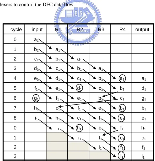
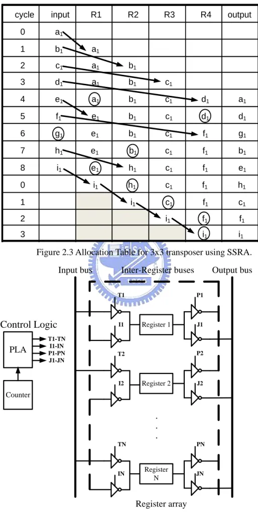
(18) Chapter 2. Fundamentals of 1-D and 2-D Register Allocation. OUT. 9l+1,2,3,4,7,8. 9l+6 9l+0,5. R1. IN. R2. R3. 9l+6. R4. 9l+0,5. Figure 2.2 Architecture of the 3x3 transposer using FBRA.. 2.2 Semi-Static Register Allocation (SSRA) The semi-static register allocation (SSRA) scheme [7-8] has been proposed to improve the number of transitions and power consumption for DFC architecture. In the same case, Figure 2.3 shows the SSRA-based allocation table for the 3x3 transposer, where arrow denotes the register transition. From Figure 2.3, the number of transitions for each iteration is 11. Using the SSRA scheme, the last input variable is required to transit from the fist register to the last register. It is observed that the transition power has been reduced; thus, the SSRA scheme results in less power consumption. Figure 2.4 shows the architecture of NxN transposer using SSRA. The global inter-register buses and I/O buses, driven by tri-state buffers, are used in the SSRA scheme to transfer data between any two registers and the I/O. Since many tri-state buffers are applied to the SSRA-based DFC design, the buffers own the large portion of area. Thus, the SSRA scheme results in large control area.. 7.
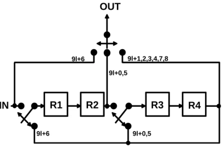
(19) Chapter 2. Fundamentals of 1-D and 2-D Register Allocation. R1. R2. cycle. input. 0. a1. 1. b1. a1. 2. c1. a1. b1. 3. d1. a1. b1. c1. 4. e1. a1. b1. c1. d1. a1. 5. f1. e1. b1. c1. d1. d1. 6. g1. e1. b1. c1. f1. g1. 7. h1. e1. b1. c1. f1. b1. 8. i1. e1. h1. c1. f1. e1. i1. h1. c1. f1. h1. i1. c1. f1. c1. i1. f1. f1. i1. i1. 0 1 2. R3. 3. R4. output. Figure 2.3 Allocation Table for 3x3 transposer using SSRA.. Input bus. Inter-Register buses T1. Control Logic PLA. T1-TN I1-IN P1-PN J1-JN. Output bus P1. Register 1. I1. J1. P2. T2. Register 2. I2. J2. Counter. TN. PN. Register N. IN. JN. Register array Figure 2.4 Architecture of the NxN transposer using SSRA. 8.
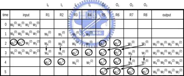
(20) Chapter 2. Fundamentals of 1-D and 2-D Register Allocation. 2.3 Two-Dimensional Register Allocation One of the 2-D register allocation schemes [4] is the extension of the FBRA scheme. It has been proposed to reduce the area of the 2-D DFC. Since 2-D register allocation scheme is used for multiple inputs and multiple outputs, it uses multiple data paths of vertical pipeline of registers and gated clocks to reduce control area overhead and power consumption. According to [4], the interface format of a DFC is defined as (m1,d1)→(m2,d2)[N]. This general format can be used to describe both word-level as well as bit-level converters. For bit-level converters, primarily used in signal processing systems, this can be read as: d1 bits of m1 words are input every input clock cycle, each having a word-length of N, while d2 bits of m2 words are output every clock cycle. For word-level converters used in two-dimensional image/video processing applications, the above format may be interpreted as: d1 samples of m1 rows of the image are input every input clock cycle, each row having N samples, and d2 samples of m2 rows are output every clock cycle. Such an input specification can be used for almost all DFC applications, except for a few like the zigzag scanner. For convenience of demonstrating the difference of the 2-D register allocation schemes, we use 1-D DWT as an example. Assume that X and Y denote the input matrix and the output matrix, respectively. w0( 0 ) (0) w Let X 4( 2 ) w0 ( 2) w4. w0( 0 ) w1( 0 ) w2( 0 ) w3( 0 ) (0) w w5( 0 ) w6( 0 ) w7( 0 ) , we obtain Y 2( 0 ) ( 2) ( 2) ( 2) w4 w1 w2 w3 (0) w5( 2 ) w6( 2 ) w7( 2 ) w6. w1( 0 ). w0( 2 ). w3( 0 ). w2( 2 ). w5( 0 ). w4( 2 ). w7( 0 ). w6( 2 ). w1( 2 ) w3( 2 ) , where the w5( 2 ) w7( 2 ) . input and output data sequences are scanned in {w0(0), w1(0), w2(0), w3(0)}, {w4(0), w5(0),. 9.
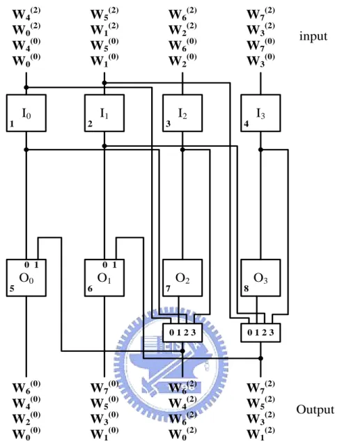
(21) Chapter 2. Fundamentals of 1-D and 2-D Register Allocation. w6(0), w7(0)}, {w0(2), w1(2), w2(2), w3(2)}, {w4(2), w5(2), w6(2), w7(2)} and {w0(0), w1(0), w0(2), w1(2)}, {w2(0), w3(0), w2(2), w3(2)}, {w4(0), w5(0), w4(2), w3(2)}, {w4(2), w5(2), w6(2), w7(2)}, respectively. Figure 2.5 shows allocation table for the 1-D discrete wavelet transform (DWT) using the 2-D register allocation. The specification of the 1-D DWT DFC can be given as (1,4)→(2,2)[8]. Figure 2.6 shows architecture for the 1-D DWT using the 2-D register allocation. The 2-D register allocation use multiple local interconnects and multiple global interconnects as well as reduce the number of interconnections by maximizing the reuse of the interconnections.. time. input. I0. I1. I2. I3. O0. O1. O2. O3. R1. R2. R3. R4. R5. R6. R7. R8. output. 0 w0(0) w1(0) w2(0) w3(0) (0). (0). (0). (0). w0(0). w1(0). w2(0). w3(0). (2). (2). (2). (2). w4(0). w5(0). w6(0). w7(0). w0(0). w1(0). w2(0). w3(0) w0(0) w1(0) w0(2) w1(2). (2). (2). (2). (2). w4(0). w5(0). w2(2). w3(3). w2(0). w3(0). w6(0). w7(0) w2(0) w3(0) w2(2) w3(2). w4(2). w5(2). w6(2). w7(2). w4(0). w5(0). w6(0). w7(0). w6(0). w7(0). w6(2). w7(2) w6(0) w7(0) w6(2) w7(2). 1 w4 w5 w6 w7. 2 w0 w1 w2 w3 3 w4 w5 w6 w7 4 5. Figure 2.5 Allocation Table for 1-D DWT using 2-D register allocation.. 10. w4(0) w5(0) w4(2) w5(2).
(22) Chapter 2. W4(2) W0(2) W4(0) W0(0). 1. I0. W5(2) W1(2) W5(0) W1(0). 2. 0 1 5. O0. W6(0) W4(0) W2(0) W0(0). I1. Fundamentals of 1-D and 2-D Register Allocation. W6(2) W2(2) W6(0) W2(0). I2. 3. W7(2) W3(2) W7(0) W3(0). 4. input. I3. 0 1 6. O1. W7(0) W5(0) W3(0) W1(0). 7. O2. 8. O3. 0123. 0123. W6(2) W4(2) W6(2) W0(2). W7(2) W5(2) W3(2) W1(2). Output. Figure 2.6 Architecture for 1-D DWT using 2-D register allocation.. 11.
(23) Chapter 3. 1-D Static Register Allocation Algorithm and Architecture. Chapter 3 1-D Static Register Allocation Algorithm and Architecture In this chapter, we explore the 1-D static register allocation (SRA) algorithm and the corresponding low-power area-efficient DFC architecture. In the same chapter, the properties for NxN matrix transposer and control unit of the 2-D DFC design are presented.. 3.1 Algorithm and Architecture Given the input time and output time of all variables. The design steps of the 1-D SRA algorithm are described as follows. Step 1: Determine the minimum number of registers using the lifetime analysis. Step 2: Assign the input variable to the available register in ascending order until exceeding the minimum number of registers. Step 3: Return to and search for the available register from the first register when exceeding the minimum number of registers. Step 4: Repeat steps 2 and 3 as required until one iteration allocation is complete. Step 5: Go to the following iterations and repeat steps 2, 3 and 4 as required until one period allocation is complete. In this thesis, the iteration is defined as the required cycles to finish a computation 12.
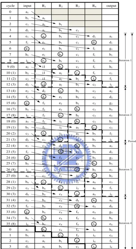
(24) Chapter 3. 1-D Static Register Allocation Algorithm and Architecture. process. The period is defined as the required cycles to finish a complete computation process, where each complete computation process has the same register allocation assignment for all variables. If the sum of life time of the corresponding variables storing at the same register is larger than the number of cycles for one iteration, the DFC possesses the feature of the multiple iterations. Otherwise, the DFC will belong to the single iteration. For the single iteration, the period has the same cycle count as the iteration. Otherwise, the period is equal to the cycles of the multiple iterations. Without loss of the generality, we use four benchmarks including 3x3 transposer, 4x4 transposer, 16x16 transposer and IIR filter to verify and demonstrate the above design steps. In the first benchmark, assume X3x3 and Y3x3 denote the input matrix and the transpose matrix of X3x3, respectively, where the relationship is expressed in (3.1). Y3 x 3 X T3 x 3 .. Let X 3 x 3. output. (3.1). a1 d1 g1. data. b1 e1 h1. c1 a1 f1 , we obtain Y3 x 3 b1 c1 i1 . sequences. are. scanned. in. d1 e1 f1. g1 h1 , where the input and i1 . {a1,b1,c1,d1,e1,f1,g1,h1,i1}. and. {a1,d1,g1,b1,e1,h1,c1,f1,i1}, respectively. The length of both sequences is nine. In step 1, using the lifetime analysis in [2], the minimum number of registers is four. In step 2, we use allocation table to assign the input variables to available registers in ascending order as shown in Figure 3.1, where arrow denotes the register transition. Thus, the input sequences {a1, b1, c1, d1} are inputted to the corresponding registers {R1, R2, R3, R4}. For next sequence data e1, we need to return to the first register and search for which register is available from R1 to R4 in step 3. In this case, R1 is available for input sequence data e1. About the next input sequence data f1, we find that R2 and R3 are not empty as shown in Figure 3.1 and then skip R2 and R3. Thus, the input data f1 is inputted to the R4 register. 13.
(25) Chapter 3 cycle. input. R1. 1-D Static Register Allocation Algorithm and Architecture R2. R3. R4. output. 0. a1. 1. b1. a1. 2. c1. a1. b1. 3. d1. a1. b1. c1. 4. e1. a1. b1. c1. d1. a1. 5. f1. e1. b1. c1. d1. d1. 6. g1. e1. b1. c1. f1. g1. 7. h1. e1. b1. c1. f1. b1. 8. i1. e1. h1. c1. f1. e1. 9 (0). a2. i1. h1. c1. f1. h1. 10 (1). b2. i1. a2. c1. f1. c1. 11 (2). c2. i1. a2. b2. f1. f1. 12 (3). d2. i1. a2. b2. c2. i1. 13 (4). e2. d2. a2. b2. c2. a2. 14 (5). f2. d2. e2. b2. c2. d2. 15 (6). g2. f2. e2. b2. c2. g2. 16 (7). h2. f2. e2. b2. c2. b2. 17 (8). i2. f2. e2. h2. c2. e2. 18 (0). a3. f2. i2. h2. c2. h2. 19 (1). b3. f2. i2. a3. c2. c2. 20 (2). c3. f2. i2. a3. b3. f2. 21 (3). d3. c3. i2. a3. b3. i2. 22 (4). e3. c3. d3. a3. b3. a3. 23 (5). f3. c3. d3. e3. b3. d3. 24 (6). g3. c3. f3. e3. b3. g3. 25 (7). h3. c3. f3. e3. b3. b3. 26 (8). i3. c3. f3. e3. h3. e3. 27 (0). a4. c3. f3. i3. h3. h3. 28 (1). b4. c3. f3. i3. a4. c3. 29 (2). c4. b4. f3. i3. a4. f3. 30 (3). d4. b4. c4. i3. a4. i3. 31 (4). e4. b4. c4. d4. a4. a4. 32 (5). f4. b4. c4. d4. e4. d4. 33 (6). g4. b4. c4. f4. e4. g4. 34 (7). h4. b4. c4. f4. e4. b4. 35 (8). i4. h4. c4. f4. e4. e4. 0. a1. h4. c4. f4. i4. h4. 1. b1. a1. c4. f4. i4. c4. 2. c1. a1. b1. f4. i4. f4. 3. d1. a1. b1. c1. i4. i4. Iteration 1. Iteration 2. Period. Iteration 3. Iteration 4. Figure 3.1 Allocation Table for 3x3 matrix transposer using 1-D SRA.. In step 4, we repeat steps 2 and 3 recursively until one iteration allocation is done as shown in Figure 3.1, where the dash-bold line denotes the boundary of one iteration. Equivalently, one computation process, 3x3 transposing, is calculated under one. 14.
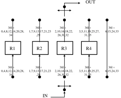
(26) Chapter 3. iteration.. 1-D Static Register Allocation Algorithm and Architecture. Finally, in step 5, we repeat steps 2, 3, 4 as required until one period. allocation is finished as shown in Figure 3.1, where the solid-bold line denotes the boundary of one period. In this case, the 3x3 transposer has nine cycles and 36 cycles for one iteration and period, respectively. From the allocation table as shown in Figure 3.1, all input variables are static in one register until they become desired outputs. Hence, this method is referred to 1-D static register allocation (SRA). According to the proposed 5-step 1-D SRA algorithm, the number of transitions can be further minimized compared with that of [2-3] and [7-8]. In this case, the numbers of transitions for each iteration handled by FBRA, SSRA, and 1-D SRA schemes are 36, 11, and 8, respectively. The corresponding new 3x3 transposer architecture is depicted in Figure 3.2. In similar behavior, the proposed 1-D SRA is capable of treating the register allocation for higher-order transposer. In the case of 4x4 transposer, the numbers of transitions for each iteration handled by FBRA, SSRA, and 1-D SRA schemes are 144, 24, and 15, respectively. For larger size case, 16x16 transposer has 57600, 570, and 255 transitions for each iteration performed by FBRA, SSRA, and 1-D SRA schemes, respectively. As a consequence, the 1-D SRA scheme can lead to lower transitions for NxN transposer. OUT. 36l + 0,4,8,12,14,20,28, 34. 36l + 1,7,9,13,17,21,23 ,29. 36l + 2,10,16,18,22, 26,30,32. 36l + 3,5,11,19,25,27, 31,35. R1. R2. R3. R4. 36l + 0,4,8,12,14,20,28, 34. 36l + 1,7,9,13,17,21,23 ,29. 36l + 2,10,16,18,22, 26,30,32. 36l + 3,5,11,19,25,27, 31,35. 36l + 6,15,24,33. 36l + 6,15,24,33. IN. Figure 3.2 Block diagram of 3x3 transposer using 1-D SRA. 15.
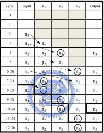
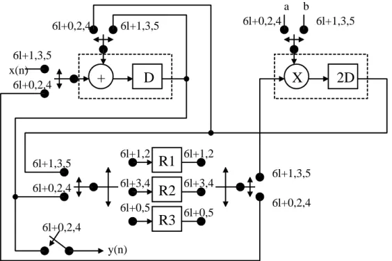
(27) Chapter 3. 1-D Static Register Allocation Algorithm and Architecture. In the fourth benchmark, IIR filter that computes y(n) = ay(n-3) + by(n-5) + x(n) is folded, we apply the SRA approach to improve the transition activities. The resulting allocation table and the improved IIR filter architecture are depicted in Figure 3.3 and 3.4, respectively, where the same notations are adopted as that in Fig. 6.19 of [2].. cycle. input. R1. R2. R3. output. 0 1 2. n2. 3. n3. n2. 4. n2. n2. n3. 5. n3. n2. n2. 6 (0). n2. n2. n2. n3. n3. 7 (1). n3. n2. n2. n2. n2. 8 (2). n2. n3. n2. n2. n3. 9 (3). n3. n2. n2. n2. n2. 10 (4). n2. n2. n3. n2. n3. 11 (5). n3. n2. n2. n2. n2. 12 (0). n2. n2. n2. n3. n3. n3. Figure 3.3 Allocation table for IIR filter using 1-D SRA.. 16.
(28) Chapter 3. 1-D Static Register Allocation Algorithm and Architecture. a 6l+0,2,4 6l+1,3,5 x(n) 6l+0,2,4. 6l+0,2,4. 6l+1,3,5. +. D. 6l+1,2. 6l+1,3,5. 6l+3,4. 6l+0,2,4. 6l+1,3,5. X. R1 R2. 6l+0,5. R3. 6l+0,2,4. b. 2D. 6l+1,2 6l+1,3,5. 6l+3,4. 6l+0,2,4. 6l+0,5. y(n). Figure 3.4 Block diagram of IIR filter using 1-D SRA.. 3.2 Properties of N x N Transposer Using 1-D SRA From the SRA-based allocation table, we observe that the periodic allocation occurs for 3x3, 4x4, and higher-order transposer. For example, if register Rj is occupied with a variable in the first cycle, then Rj owns the identical variable in (l + CP)-th cycle, where CP denotes the number of cycles for one period. We can calculate CP by the following properties 2 and 3. Without loss of the generality, the relationship of the NxN input matrix and transposed matrix can be expressed in (3.2).. YN N XTN N. a1,1 a 2,1 a N ,1. a a a. 1, 2 2, 2. N ,2. T. a1,1 a 2, N 1, 2 a1, N N,N . a a a. 1, N. a a a. We can derive the following properties for NxN transposer. 17. 2 ,1. 2, 2. 2, N. N ,2 N,N . a a a. N ,1. (3.2).
(29) Chapter 3. 1-D Static Register Allocation Algorithm and Architecture. Property 1: The number of registers NR equals (N-1)2 for NxN transposer. Proof: Input and output data sequences in (3.2) can be scanned in the following. X s {a1,1 , a1,2 ,..., a1, N , a2,1 , a2,2 ,..., a 2, N ,..., a N ,1 ,..., a N , N }. (3.3a). Ys {a1,1 , a 2,1 ,..., a N ,1 , a1,2 , a 2,2 ,..., a N ,2 ,..., a1, N ,..., a N , N }. (3.3b). From (3.3a) and (3.3b), since NxN transposer is a causal system, we need to shift right the transposed sequence in (3.3b). The variable in (3.3a) compared with that in (3.3b) which has the longest distance will be the aligned point. In this general case, a N ,1 is the aligned point. Thus, the shift-right distance implemented by registers is equal to the number of registers for NxN transposer. Hence, the required number of registers can be presented in (3.4). N R N ( N 1) 1 N ( N 1) 2 .. ◆. (3.4). Property 2: The number of cycles for one iteration, CI, equals N2 for NxN transposer. Proof: According to the iteration definition and allocation table as addressed in this chapter, we can see that each iteration consumes the cycles equaling the total number of variables in the transposer. Thus, for NxN transposer, the number of cycles for each iteration can be expressed in (3.5). CI N 2 .. ◆. (3.5). Under the multiple-iteration case (i.e., N 3 ), we can obtain Property 3. Property 3: The number of iterations for one period, IP, equals 2(N-1) for NxN transposer. Proof: For convenience of derivation, the input matrix X is repeated in (3.6).. 18.
(30) Chapter 3. a1,1 a2,1 a3,1 a XNxNX= 4,1 aN-2,1. aN-1,1 a N,1 . 1-D Static Register Allocation Algorithm and Architecture. a a a a. a a a a. a a a a. a a a. a a a. a a a. 1,2 2,2 3,2 4,2. N-2,2 N-1,2 N,2. 1,3 2,3 3,3 4,3. N-2,3. N-1,3 N,3. 1,4 2,4 3,4 4,4. N-2,4 N-1,4 N,4. a a a a a a a a a a a a a a 1,5. 1,6. 2,5. 2,6. 3,5. 3,6. 4,5. 4,6. N-2,5. N-2,5 . N-1,5. N-1,5. N,5. N,6. a a a a. 2, N 3, N 4, N . 1, N. a a a. N-1,N N, N . N-2,N. (3.6). At the first iteration, from input sequence in (3.3a) and aligned output sequence of (3.3b), the output variable a1,1 occurs at the same time instance as the input variable aN-1, 2.. Similarly, the output variable aN-1,2 occurs at the same time instance as the input. variable aN,N. These three variables are certainly allocated at the same register, R1. That means the input variable a1,1 at the next iteration cannot be allocated at R1 register and moved to R2 register. At the second and third iteration, the new first input variable a1,1 has to be fed into the next available register R2 and R3, respectively, via SRA approach. For N=3, at the forth iteration, the new first input variable a1,1 has to be fed into the available register R4 (i.e., a4 is fed into R4 as shown in Figure 3.1). However, for N 4 , at the fourth iteration, the first input variable will encounter the unavailable register R 4 that is occupied by other variable. That means R4 register has longer life time while the input variable a1,1 is arriving. For instance, we show the allocation table of 4x4 transposer in Figure 3.3 to illustrate the above situation. In this case, a1,1 is needed to input to available register R7 and each input variable will be only appeared in dedicated registers for N 4 . As a consequence, the input variables can be separated into Q groups (i.e., G1, G2, …, GQ) to finish the allocation. In the case of 4x4 transposer, there exist two groups in Figure 3.5. The group G1 is composed of R1, R2, R3, R7, R8, R9 and the group G2 consists of R4, R5,. 19.
(31) Chapter 3. 1-D Static Register Allocation Algorithm and Architecture. R6 . After transposing the NxN matrix, at the first iteration, some registers store multiple variables and some registers store single variable. The sum of the lifetime of all variables stored at the register under the first iteration boundary can be longer than CI, less than (CI -1), or equal to CI and (CI -1). Thus, the utilized registers from R1 to R(N-1)2 can be classified into five types. The lifetime of one register storing the single variable is longer than CI and then is referred to as type-1 register. The lifetime of one register storing multiple variables is longer than CI, and then is named as type-2 register. The lifetime of one register storing the single variable is equal to (CI -1), and then is referred to as type-3 register. The lifetime of one register storing multiple variables is equal to (CI -1), and then is named as type-4 register. The lifetime of one register storing the single variable is less than (CI -1), and then is referred to as type-5 register. Thus, for N 3 , the difference value of the type-3, and 4 register can be defined as the sum of the. lifetime of all variables storing in this register in (3.7). DRi C LT , Ri C I 1 .. (3.7). where C LT , Ri denotes the life time of the register Ri. For a1,1, it belongs to the type-2 register; from Property 1, the difference cycle Da1,1 is (N-1)2 due to the shift distance. For other input variables marked in dash-line circle, they belong to the type-3 and 4 registers. The difference values of the corresponding registers are equal to zero in (3.7), where the specified input variables ai,j are allocated at R((i-1)xN+j). According to the above calculation, the input variable belongs to which register can be determined.. 20.
(32) Chapter 3 cycle. input. R1. R2. R3. 1-D Static Register Allocation Algorithm and Architecture R4. R5. R6. R7. R8. R9. output. 0. a1,1. 1. a1,2. a1,1. 2. a1,3. a1,1. a1,2. 3. a1,4. a1,1. a1,2. a1,3. 4. a2,1. a1,1. a1,2. a1,3. a1,4. 5. a2,2. a1,1. a1,2. a1,3. a1,4. a2,1. 6. a2,3. a1,1. a1,2. a1,3. a1,4. a2,1. a2,2. 7. a2,4. a1,1. a1,2. a1,3. a1,4. a2,1. a2,2. a2,3. 8. a3,1. a1,1. a1,2. a1,3. a1,4. a2,1. a2,2. a2,3. a2,4. 9. a3,2. a1,1. a1,2. a1,3. a1,4. a2,1. a2,2. a2,3. a2,4. a3,1. a1,1. 10. a3,3. a3,2. a1,2. a1,3. a1,4. a2,1. a2,2. a2,3. a2,4. a3,1. a2,1. 11. a3,4. a3,2. a1,2. a1,3. a1,4. a3,3. a2,2. a2,3. a2,4. a3,1. a3,1. 12. a4,1. a3,2. a1,2. a1,3. a1,4. a3,3. a2,2. a2,3. a2,4. a3,4. a4,1. 13. a4,2. a3,2. a1,2. a1,3. a1,4. a3,3. a2,2. a2,3. a2,4. a3,4. a1,2. 14. a4,3. a3,2. a4,2. a1,3. a1,4. a3,3. a2,2. a2,3. a2,4. a3,4. a2,2. 15. a4,4. a3,2. a4,2. a1,3. a1,4. a3,3. a4,3. a2,3. a2,4. a3,4. a3,2. 16 (0). a1,1. a4,4. a4,2. a1,3. a1,4. a3,3. a4,3. a2,3. a2,4. a3,4. a4,2. 17 (1). a1,2. a4,4. a1,1. a1,3. a1,4. a3,3. a4,3. a2,3. a2,4. a3,4. a1,3. 18 (2). a1,3. a4,4. a1,1. a1,2. a1,4. a3,3. a4,3. a2,3. a2,4. a3,4. a2,3. 19 (3). a1,4. a4,4. a1,1. a1,2. a1,4. a3,3. a4,3. a1,3. a2,4. a3,4. a3,3. 20 (4). a2,1. a4,4. a1,1. a1,2. a1,4. a1,4. a4,3. a1,3. a2,4. a3,4. a4,3. 21 (5). a2,2. a4,4. a1,1. a1,2. a1,4. a1,4. a2,1. a1,3. a2,4. a3,4. a1,4. 22 (6). a2,3. a4,4. a1,1. a1,2. a2,2. a1,4. a2,1. a1,3. a2,4. a3,4. a2,4. 23 (7). a2,4. a4,4. a1,1. a1,2. a2,2. a1,4. a2,1. a1,3. a2,3. a3,4. a3,4. 24 (8). a3,1. a4,4. a1,1. a1,2. a2,2. a1,4. a2,1. a1,3. a2,3. a2,4. a4,4. 25 (9). a3,2. a3,1. a1,1. a1,2. a2,2. a1,4. a2,1. a1,3. a2,3. a2,4. a1,1. 26(10). a3,3. a3,1. a3,2. a1,2. a2,2. a1,4. a2,1. a1,3. a2,3. a2,4. a2,1. 27(11). a3,4. a3,1. a3,2. a1,2. a2,2. a1,4. a3,3. a1,3. a2,3. a2,4. a3,1. 28(12). a4,1. a3,4. a3,2. a1,2. a2,2. a1,4. a3,3. a1,3. a2,3. a2,4. a4,1. 29(13). a4,2. a3,4. a3,2. a1,2. a2,2. a1,4. a3,3. a1,3. a2,3. a2,4. a1,2. 30(14). a4,3. a3,4. a3,2. a4,2. a2,2. a1,4. a3,3. a1,3. a2,3. a2,4. a2,2. 31(15). a4,4. a3,4. a3,2. a4,2. a4,3. a1,4. a3,3. a1,3. a2,3. a2,4. a3,2. 32 (0). a1,1. a3,4. a4,4. a4,2. a4,3. a1,4. a3,3. a1,3. a2,3. a2,4. a4,2. 33 (1). a1,2. a3,4. a4,4. a1,1. a4,3. a1,4. a3,3. a2,3. a2,4. a1,3. 34 (2). a1,3. a3,4. a4,4. a1,1. a4,3. a1,4. a3,3. a1,3 a1,2. a2,3. a2,4. a2,3. 35 (3). a1,4. a3,4. a4,4. a1,1. a4,3. a1,4. a3,3. a1,2. a1,3. a2,4. a3,3. 36 (4). a2,1. a3,4. a4,4. a1,1. a4,3. a1,4. a1,4. a1,2. a1,3. a2,4. a4,3. 37 (5). a2,2. a3,4. a4,4. a1,1. a2,1. a1,4. a1,4. a1,2. a1,3. a2,4. a1,4. 38 (6). a2,3. a3,4. a4,4. a1,1. a2,1. a2,2. a1,4. a1,2. a1,3. a2,4. a2,4. 39 (7). a2,4. a3,4. a4,4. a1,1. a2,1. a2,2. a1,4. a1,2. a1,3. a2,3. a3,4. 40 (8). a3,1. a2,4. a4,4. a1,1. a2,1. a2,2. a1,4. a1,2. a1,3. a2,3. a4,4. 41 (9). a3,2. a2,4. a3,1. a1,1. a2,1. a2,2. a1,4. a1,2. a1,3. a2,3. a1,1. 42(10). a3,3. a2,4. a3,1. a3,2. a2,1. a2,2. a1,4. a1,2. a1,3. a2,3. a2,1. 43(11). a3,4. a2,4. a3,1. a3,2. a3,3. a2,2. a1,4. a1,2. a1,3. a2,3. a3,1. 44(12). a4,1. a2,4. a3,4. a3,2. a3,3. a2,2. a1,4. a1,2. a1,3. a2,3. a4,1. 45(13). a4,2. a2,4. a3,4. a3,2. a3,3. a2,2. a1,4. a1,2. a1,3. a2,3. a1,2. 46(14). a4,3. a2,4. a3,4. a3,2. a3,3. a2,2. a1,4. a4,2. a1,3. a2,3. a2,2. 47(15). a4,4. a2,4. a3,4. a3,2. a3,3. a4,3. a1,4. a4,2. a1,3. a2,3. a3,2. 48 (0). a1,1. a2,4. a3,4. a4,4. a3,3. a4,3. a1,4. a4,2. a1,3. a2,3. a4,2. 49 (1). a1,2. a2,4. a3,4. a4,4. a3,3. a4,3. a1,4. a1,1. a1,3. a2,3. a1,3. 50 (2). a1,3. a2,4. a3,4. a4,4. a3,3. a4,3. a1,4. a1,1. a1,2. a2,3. a2,3. 51 (3). a1,4. a2,4. a3,4. a4,4. a3,3. a4,3. a1,4. a1,1. a1,2. a1,3. a3,3. 52 (4). a2,1. a2,4. a3,4. a4,4. a1,4. a4,3. a1,4. a1,1. a1,2. a1,3. a4,3. 53 (5). a2,2. a2,4. a3,4. a4,4. a1,4. a2,1. a1,4. a1,1. a1,2. a1,3. a1,4. 54 (6). a2,3. a2,4. a3,4. a4,4. a1,4. a2,1. a2,2. a1,1. a1,2. a1,3. a2,4. 55 (7). a2,4. a2,3. a3,4. a4,4. a1,4. a2,1. a2,2. a1,1. a1,2. a1,3. a3,4. 56 (8). a3,1. a2,3. a2,4. a4,4. a1,4. a2,1. a2,2. a1,1. a1,2. a1,3. a4,4. 21. Iteration 1. Iteration 2. Iteration 3.
(33) Chapter 3. 1-D Static Register Allocation Algorithm and Architecture. 56 (8). a3,1. a2,3. a2,4. a4,4. a1,4. a2,1. a2,2. a1,1. a1,2. a1,3. a4,4. 57 (9). a3,2. a2,3. a2,4. a3,1. a1,4. a2,1. a2,2. a1,1. a1,2. a1,3. a1,1. 58(10). a3,3. a2,3. a2,4. a3,1. a1,4. a2,1. a2,2. a3,2. a1,2. a1,3. a2,1. 59(11). a3,4. a2,3. a2,4. a3,1. a1,4. a3,3. a2,2. a3,2. a1,2. a1,3. a3,1. 60(12). a4,1. a2,3. a2,4. a3,4. a1,4. a3,3. a2,2. a3,2. a1,2. a1,3. a4,1. 61(13). a4,2. a2,3. a2,4. a3,4. a1,4. a3,3. a2,2. a3,2. a1,2. a1,3. a1,2. 62(14). a4,3. a2,3. a2,4. a3,4. a1,4. a3,3. a2,2. a3,2. a4,2. a1,3. a2,2. 63(15). a4,4. a2,3. a2,4. a3,4. a1,4. a3,3. a4,3. a3,2. a4,2. a1,3. a3,2. a2,4. a3,4. a4,2. a1,3. a4,2. a1,1. a2,3. a1,4. a3,3. a4,3. a4,4. 65 (1). a1,2. a2,3. a2,4. a3,4. a1,4. a3,3. a4,3. a4,4. a1,1. a1,3. a1,3. 66 (2). a1,3. a2,3. a2,4. a3,4. a1,4. a3,3. a4,3. a4,4. a1,1. a1,2. a2,3. a1,3. a2,4. a1,4. a3,3. a4,3. a4,4. a1,1. a1,2. a3,3. a3,4. a1,4. a1,4. a4,3. a4,4. a1,1. a1,2. a4,3. a3,4. a1,4. a1,4. a2,1. a4,4. a1,1. a1,2. a1,4. a1,1. a1,2. a2,4. 64 (0). 67 (3). a1,4. a3,4. 68 (4). a2,1. a1,3. a2,4. 69 (5). a2,2. a1,3. a2,4. a3,4. a2,2. a1,4. a2,1. a4,4. a3,4. a2,2. a1,4. a2,1. a4,4. a1,1. a1,2. a3,4. 70 (6). a2,3. a1,3. a2,4. 71 (7). a2,4. a1,3. a2,3. 72 (8). a3,1. a1,3. a2,3. a2,4. a2,2. a1,4. a2,1. a4,4. a1,1. a1,2. a4,4. 73 (9). a3,2. a1,3. a2,3. a2,4. a2,2. a1,4. a2,1. a3,1. a1,1. a1,2. a1,1. 74(10). a3,3. a1,3. a2,3. a2,4. a2,2. a1,4. a2,1. a3,1. a3,2. a1,2. a2,1. 75(11). a3,4. a1,3. a2,3. a2,4. a2,2. a1,4. a3,3. a3,1. a3,2. a1,2. a3,1. 76(12). a4,1. a1,3. a2,3. a2,4. a2,2. a1,4. a3,3. a3,4. a3,2. a1,2. a4,1. 77(13). a4,2. a1,3. a2,3. a2,4. a2,2. a1,4. a3,3. a3,4. a3,2. a1,2. a1,2. 78(14). a4,3. a1,3. a2,3. a2,4. a2,2. a1,4. a3,3. a3,4. a3,2. a4,2. a2,2. 79(15). a4,4. a1,3. a2,3. a2,4. a4,3. a1,4. a3,3. a3,4. a3,2. a4,2. a3,2. 80 (0). a1,1. a1,3. a2,3. a2,4. a4,3. a1,4. a3,3. a3,4. a4,4. a4,2. a4,2. 81 (1). a1,2. a1,3. a2,3. a2,4. a4,3. a1,4. a3,3. a3,4. a4,4. a1,1. a1,3. 82 (2). a1,3. a1,2. a2,3. a2,4. a4,3. a1,4. a3,3. a3,4. a4,4. a1,1. a2,3. 83 (3). a1,4. a1,2. a1,3. a2,4. a4,3. a1,4. a3,3. a3,4. a4,4. a1,1. a3,3. 84 (4). a2,1. a1,2. a1,3. a2,4. a4,3. a1,4. a1,4. a3,4. a4,4. a1,1. a4,3. 85 (5). a2,2. a1,2. a1,3. a2,4. a2,1. a1,4. a1,4. a3,4. a4,4. a1,1. a1,4. 86 (6). a2,3. a1,2. a1,3. a2,4. a2,1. a2,2. a1,4. a3,4. a4,4. a1,1. a2,4. 87 (7). a2,4. a1,2. a1,3. a2,3. a2,1. a2,2. a1,4. a3,4. a4,4. a1,1. a3,4. 88 (8). a3,1. a1,2. a1,3. a2,3. a2,1. a2,2. a1,4. a2,4. a4,4. a1,1. a4,4. 89 (9). a3,2. a1,2. a1,3. a2,3. a2,1. a2,2. a1,4. a2,4. a3,1. a1,1. a1,1. 90(10). a3,3. a1,2. a1,3. a2,3. a2,1. a2,2. a1,4. a2,4. a3,1. a4,3. a2,1. 91(11). a3,4. a1,2. a1,3. a2,3. a3,3. a2,2. a1,4. a2,4. a3,1. a4,3. a3,1. 92(12). a4,1. a1,2. a1,3. a2,3. a3,3. a2,2. a1,4. a2,4. a3,4. a4,3. a4,1. 93(13). a4,2. a1,2. a1,3. a2,3. a3,3. a2,2. a1,4. a2,4. a3,4. a4,3. a1,2. 94(14). a4,3. a4,2. a1,3. a2,3. a3,3. a2,2. a1,4. a2,4. a3,4. a4,3. a2,2. 95(15). a4,4. a4,2. a1,3. a2,3. a3,3. a4,3. a1,4. a2,4. a3,4. a4,3. a3,2. 0. a1,1. a4,2. a1,3. a2,3. a3,3. a4,3. a1,4. a2,4. a3,4. a4,4. a4,2. 1. a1,2. a1,1. a1,3. a2,3. a3,3. a4,3. a1,4. a2,4. a3,4. a4,4. a1,3. 2. a1,3. a1,1. a1,2. a2,3. a3,3. a4,3. a1,4. a2,4. a3,4. a4,4. a2,3. 3. a1,4. a1,1. a1,2. a1,3. a3,3. a4,3. a1,4. a2,4. a3,4. a4,4. a3,3. 4. a2,1. a1,1. a1,2. a1,3. a1,4. a4,3. a1,4. a2,4. a3,4. a4,4. a4,3. 5. a2,2. a1,1. a1,2. a1,3. a1,4. a2,1. a1,4. a2,4. a3,4. a4,4. a1,4. 6. a2,3. a1,1. a1,2. a1,3. a1,4. a2,1. a2,2. a2,4. a3,4. a4,4. a2,4. 7. a2,4. a1,1. a1,2. a1,3. a1,4. a2,1. a2,2. a2,3. a3,4. a4,4. a3,4. 8. a3,1. a1,1. a1,2. a1,3. a1,4. a2,1. a2,2. a2,3. a2,4. a4,4. a4,4. Iteration 4. Iteration 5. Iteration 6. Figure 3.5 Allocation table for 4x4 transposer using 1-D SRA.. The difference of the type-1 and type-5 registers can be calculated from the. 22.
(34) Chapter 3. 1-D Static Register Allocation Algorithm and Architecture. corresponding variables owing to the single variable. The difference of type-1 register designated by square box as shown in (3.6) can be generally represented in (3.8). Dai ,i k 3 CLT , ai , i k 3 CI (k 1)( N 1). (3.8). for 1 i ( N k 3), k 0,1,2,..., ( N 4), and N 4. where CLT , ai , j denotes the life time of the input variable ai,j. Each detailed equation can be obtained from (3.8) as follows. Da1,4 = Da2,5 = ... = DaN-3,N = (N-1), Da1,5 = Da2,6 = ... = DaN-4,N = 2(N-1), Da1,6 = Da2,7 = ... = DaN-5,N = 3(N-1), ..., Da1,N = (N-3)(N-1), where ai,j will be allocated at R((i-1)xN+j). In similar behavior, at the first iteration, the difference of each type-5 register designated by circle box as shown in (3.6) can be generally represented in (3.9). Daik 1,i2 C LT ,aik 1,i2 C I (k 1)( N 1). (3.9). for 1 i ( N k 3), k 0,1,2,..., ( N 4), N 4. Each detailed equation can be obtained from (3.9) as follows. Da2,3 = Da3,4 =...= DaN-2,N-1 = -(N-1), Da3,3 = Da4,4 = ... = DaN-2,N-2 = -2(N-1), ..., DaN-2,3 = -(N-3)(N-1), where ai,j will be allocated at R((i-1)xN+j). Note that, for 3x3 transposer, equations (3.8) and (3.9) do not exist. According to (3.7), (3.8) and (3.9), we can calculate matrix D in (3.10) to represent the relationship of difference of registers.. DR D R DR DR XNxNX= D DR. D D D D D D D D D D D D D D x x x x x x x x x x x 1. N+1. 2N+1. 3N+1. D D D D. (N-3)N+1. R2. RN+2. R2N+2. R3N+2. R(N-3)N+2. D D D D. R3. RN+3. R2N+3. R3N+3. D D D D. R4. R5. R6. RN+4. RN+5. RN+6. R2N+4. R2N+5. R2N+6. R3N+4. R3N+5. R3N+6. D D D D. R2N. R3N. R4N. D x x. R(N-3)N+3 R(N-3)N+4 R(N-3)N+5 R (N-3)N+6. R(N-2)N+1. 23. RN. . R(N-2)N. . (3.10).
(35) Chapter 3. 1-D Static Register Allocation Algorithm and Architecture. In (3.6), G1 group as designated by diamond box consists of the input variables a1,1, a1,2, a1,3, a2,3, a2,4,..., aN-2,N-1, aN-2,N, aN-1,1. Using (3.6), (3.7), (3.8), (3.9) and (3.10), the cycles of DG1 can be derived as DG1 DR1 DR 2 DR 3 ... DR ( N 2 2 N 1) DaN 2, N 1 DR ( N 1) 2 DR1 DR 2 DR 3 ... DR ( N 2 2 N 1) DR ( N ( N 2)) DR ( N 1) 2 ( N 1) 2 ( N 3)( N 1) 2( N 1) ,. N 3. (3.11). where DG1 denotes the sum of difference cycles of registers in G1 group. However, it is difficult to formulate the relationship between difference value of DG of other group and order N. From (3.10), the value of DG will be consumed by DG iterations. That means one complete periodic allocation process can be finished after D G1 iterations. Thus, we obtain (3.11) as follows. I P 2( N 1) ,. N 3.. ◆. (3.12). Example 1: For 3x3 transposer whose input matrix is shown in (3.13), at the first iteration, the life time cycle of each register is listed from (3.14a) to (3.14d) and the 3x3 matrix D is shown in (3.15).. a a a. 1,1. X3x3 =. 2,1 3,1. a a a. 1,2 2,2 3,2. a a a. 1,3 2,3 3,3. (3.13). and DR1 = 13 - 9 = 4,. (3.14a). DR2 = 9 - 9 = 0,. (3.14b). DR3 = 9 - 9 = 0,. (3.14c). DR4 = 9 - 9 = 0.. (3.14d). 24.
(36) Chapter 3. D3x3 =. 4 0 x. 0 x x. 1-D Static Register Allocation Algorithm and Architecture. 0 x x. (3.15). In this case, the group G1 consists of R1, R2, R3, and R4. We obtain the number of iterations by summing (3.14a) to (3.14d). Ip=DG1=DR1+DR2+DR3+DR4=4. Thus, we require four iterations to complete one period allocation for 3x3 transposer.. ◆. Example 2: For 4x4 transposer whose input matrix is shown in (3.16), at the first iteration, the life time cycle of each register is listed from (3.17a) to (3.17i) and the 4x4 matrix R is shown in (3.18).. a a a a. 1,1. X4x4 =. 2,1 3,1 4,1. a a a a. 1,2 2,2 3,2 4,2. a a a a. 1,3 2,3 3,3 4,3. a a a a. 1,4 2,4 3,4 4,4. (3.16). and DR1 = 25 – 16 = 9,. (3.17a). DR2 = 16 – 16 = 0,. (3.17b). DR3 = 16 – 16 = 0,. (3.17c). DR4 = 19 – 16 = 3,. (3.17d). DR5 = 16 – 16 = 0,. (3.17e). DR6 = 16 – 16 = 0,. (3.17f). DR7 = 13 – 16 = -3,. (3.17g). DR8 = 16 – 16 = 0,. (3.17h). DR9 = 16 – 16 = 0,. (3.17i). 25.
(37) Chapter 3. D4x4 =. 9 0 0 x. 0 0 0 -3 x x x x. 1-D Static Register Allocation Algorithm and Architecture. 3 0 x x. (3.18). Note that there exist two groups. The group G1 is composed of R1, R2, R3, R7, R8, R9 and the group G2 consists of R4, R5, R6. We obtain the number of iterations by summing (3.17a), (3.17b), (3.17c), (3.17g), (3.17h), and (3.17i). Ip = DG1 = DR1 + DR2 + DR3 + DR7 + DR8 + DR9 = 9-3x1= 6. Thus, we require six iterations to complete one period ◆. allocation for 4x4 transposer.. Hence, we are able to calculate the number of cycles for one period via multiplying (3.5) and (3.12) for multiple iterations as expressed in upper part of (3.19). For single iteration, CP=CI as expressed in lower part of (3.19). 2 N 2 ( N 1) for N 3 CP . 2 for N 2 CI N. (3.19). In the case of the 3x3 transposer, we can directly use (3.19) to calculate the number of cycles for one period (i.e., CP = 36).. 3.3 Control Unit of DFC Using 1-D SRA The control unit of DFC designs affects the control area size and power consumption of the DFC design. Since the control unit of the 1-D SRA-based design has to handle multiple iterations (one period), the control overhead is larger than that of the conventional designs. The signals generated by control unit are responsible for controlling the multiplexor and register writing. Since the control signal can be 26.
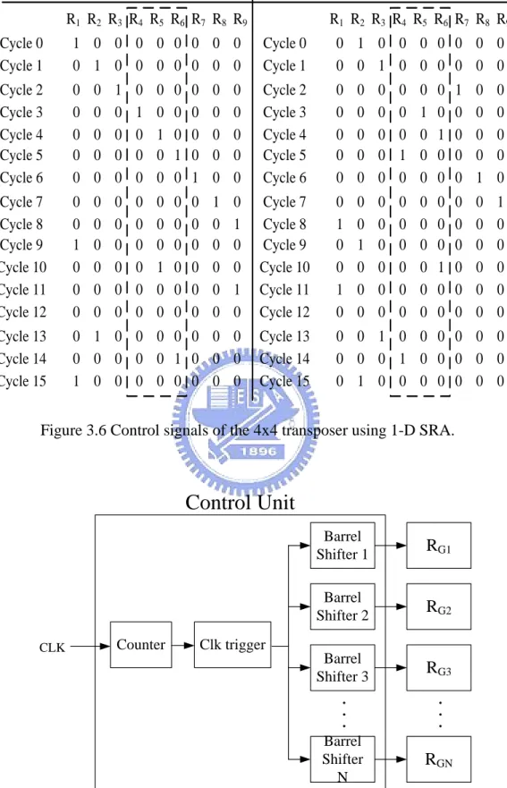
(38) Chapter 3. 1-D Static Register Allocation Algorithm and Architecture. partitioned to several groups, the number of groups depends on the size of the DFC design (i.e., the 4x4 transposer with two groups). In the multiple-iteration case, the group control signal bits of the second iteration can be obtained by rotating right 1-bit of the group control signal bits of the first iteration. The group control signal bits of the third iteration can be obtained by rotating right 1-bit of the group control signal bits of the second iteration and so forth until the last iteration. An example is shown in Figure 3.6. According to the above analysis, we can use barrel shifters to reduce overhead and complexity of the control unit. The architecture of control unit using SRA is shown in Figure 3.7. The architecture of 4x4 transposer using SRA is shown in Figure 3.8. Compared with SSRA, the input ports of all registers connect to data input port of the top module to reduce control overhead and each writing signal of register is independently generated by iteration based control unit.. 27.
(39) Chapter 3. 1-D Static Register Allocation Algorithm and Architecture. The control signal of Iteration 1 :. The control signal of Iteration 2 :. R1 R2 R3 R4 R5 R6 R7 R8 R9. R1 R2 R3 R4 R5 R6 R7 R8 R9. Cycle 0 Cycle 1. 1 0 0 0 0 0 0 0 0 0 1 0 0 0 0 0 0 0. Cycle 0 Cycle 1. 0 1 0 0 0 0 0 0 0 0 0 1 0 0 0 0 0 0. Cycle 2 Cycle 3 Cycle 4 Cycle 5 Cycle 6. 0 0 0 0 0. 0 0 0 0 0. 1 0 0 0 0. 0 1 0 0 0. 0 0 1 0 0. 0 0 0 1 0. 0 0 0 0 1. 0 0 0 0 0. 0 0 0 0 0. Cycle 2 Cycle 3 Cycle 4 Cycle 5 Cycle 6. 0 0 0 0 0. 0 0 0 0 0. 0 0 0 0 0. 0 0 0 1 0. 0 1 0 0 0. 0 0 1 0 0. 1 0 0 0 0. 0 0 0 0 1. 0 0 0 0 0. Cycle 7 Cycle 8 Cycle 9 Cycle 10 Cycle 11 Cycle 12. 0 0 1 0 0 0. 0 0 0 0 0 0. 0 0 0 0 0 0. 0 0 0 0 0 0. 0 0 0 1 0 0. 0 0 0 0 0 0. 0 0 0 0 0 0. 1 0 0 0 0 0. 0 1 0 0 1 0. Cycle 7 Cycle 8 Cycle 9 Cycle 10 Cycle 11 Cycle 12. 0 1 0 0 1 0. 0 0 1 0 0 0. 0 0 0 0 0 0. 0 0 0 0 0 0. 0 0 0 0 0 0. 0 0 0 1 0 0. 0 0 0 0 0 0. 0 0 0 0 0 0. 1 0 0 0 0 0. Cycle 13 Cycle 14 Cycle 15. 0 1 0 0 0 0 0 0 0 0 0 0 0 0 1 0 0 0 1 0 0 0 0 0 0 0 0. Cycle 13 Cycle 14 Cycle 15. 0 0 1 0 0 0 0 0 0 0 0 0 1 0 0 0 0 0 0 1 0 0 0 0 0 0 0. Figure 3.6 Control signals of the 4x4 transposer using 1-D SRA.. Control Unit. CLK. Counter. Barrel Shifter 1. RG1. Barrel Shifter 2. RG2. Barrel Shifter 3. RG3. Barrel Shifter N. RGN. Clk trigger. Figure 3.7 Architecture of control unit of DFC using 1-D SRA.. 28.
(40) Chapter 3. 1-D Static Register Allocation Algorithm and Architecture. DIN[N:0] R1. R2. R3. R4 M Control Unit (iteration based). R5. R6. U. DOUT[N:0]. X. R7. CLK. R8. R9. Figure 3.8 Architecture of 4x4 transposer using 1-D SRA.. 29.
(41) Chapter 4. 2-D Static Register Allocation Algorithm and Architecture. Chapter 4 2-D Static Register Allocation Algorithm and Architecture In this chapter, we propose the 2-D static register allocation (2-D SRA) algorithm and the corresponding low-power area-efficient 2-D DFC architecture. In the same chapter, the properties for NxN par-transposer and control unit of the 2-D DFC design are presented.. 4.1 Algorithm and Architecture According to [4], the throughput of the 2-D DFC is maintained constant, i.e., the input and output data rates are the same. From the given specifications, the number of data samples input in every input clock cycle = m1 d1 , while the number of samples output in every output clock cycle = m2 d 2 . Thus, if g = gcd( m1 d1 , m2 d 2 ), then the input cycle period = (m1 d1 ) / g and the output cycle period = (m2 d 2 ) / g . This ensures that the number of samples input and output from the DFC for every clock cycle remains constant at g samples per time unit. The design steps of the 2-D SRA algorithm are described as follows. Step 1: Determine the minimum number of registers using the lifetime analysis. Step 2: Assign the input variables to the available registers in ascending order until exceeding the minimum number of registers. 30.
(42) Chapter 4. 2-D Static Register Allocation Algorithm and Architecture. Step 3: Return to and search for the available registers from the first register when exceeding the minimum number of registers. Allocate the corresponding variable to the same register when the variable of the last iteration stores at the register. Allocate the variable with the shorter lifetime to the register with the lower index and allocate other variables with the longer lifetime to the next register with larger index in ascending order. Step 4: Repeat steps 2 and 3 as required until one iteration allocation is complete. Step 5: Go to the following iterations and repeat steps 2, 3 and 4 as required until one period allocation is complete. In this chapter, the iteration is defined as the required cycles to finish a computation process. The period is defined as the required cycles to finish a complete computation process, where each complete computation process has the same register allocation assignment for all variables. If the sum of life time of the corresponding variables storing at the same register is larger than the number of cycles for one iteration, the DFC possesses the feature of the multiple iterations. Otherwise, the DFC will belong to the single iteration. For single iteration, the period has the same cycle count as the iteration. Otherwise, the period is equal to the cycles of the multiple iterations. Without loss of the generality, we use four benchmarks including 1-D discrete wavelet transform (DWT), zigzag scanner, 4x4 par-transposer and 16x16 par-transposer to verify and demonstrate the above design steps. The DFC of 1-D DWT is being increasing used as a tool for multiscale analysis for image compress application [12]. The DFC of 1-D DWT is used to reorganize the data from the filter at the lower resolution level to be fed into the low-pass and high-pass filters of the next resolution level. The specification of the DFC of 1-D DWT can be given as (1,4) →(2,2)[8]. Note that the period of computation is four cycles, and four samples are processed each clock cycle. 31.
(43) Chapter 4. 2-D Static Register Allocation Algorithm and Architecture. In the first benchmark, assume X and Y denote the input matrix and the output matrix, respectively. w0( 0 ) (0) w Let X 4( 2 ) w0 ( 2) w4. w0( 0 ) w1( 0 ) w2( 0 ) w3( 0 ) (0) w w5( 0 ) w6( 0 ) w7( 0 ) , we obtain Y 2( 0 ) ( 2) ( 2) ( 2) w4 w1 w2 w3 (0) ( 2) ( 2) ( 2) w5 w6 w7 w6. w1( 0 ). w0( 2 ). w3( 0 ). w2( 2 ). w5( 0 ). w4( 2 ). w7( 0 ). w6( 2 ). w1( 2 ) w3( 2 ) , where the w5( 2 ) w7( 2 ) . input and output data sequences are scanned in {w0(0), w1(0), w2(0), w3(0)}, {w4(0), w5(0), w6(0), w7(0)}, {w0(2), w1(2), w2(2), w3(2)}, {w4(2), w5(2), w6(2), w7(2)} and {w0(0), w1(0), w0(2), w1(2)}, {w2(0), w3(0), w2(2), w3(2)}, {w4(0), w5(0), w4(2), w3(2)}, {w4(2), w5(2), w6(2), w7(2)}, respectively. The length of both sequences is four. In step 1, using the lifetime analysis in [2], the minimum number of registers is eight. In step 2, we use allocation table to assign the input variables to available registers in ascending order as shown in Figure 4.1. Thus, the input sequences {w0(0), w1(0), w2(0), w3(0)} and {w4(0), w5(0), w6(0), w7(0)} are inputted to the corresponding registers {R1, R2, R3, R4} and {R5, R6, R7, R8}. For next sequence data w2(2) and w3(2), we need to return to the first register and search for which register is available from R1 to R8 in step 3. In this case, R1 and R2 are available for input sequence data w2(2) and w3(2). About the next input sequences data {w4(2), w5(2), w6(2), w7(2)}, we find that R1, R2, R3 and R4 are not empty as shown in Figure 4.1. From step 3, since the lifetime of w4(2) and w5(2) is shorter than the lifetime of w6(2) and w7(2), the input data w4(2) and w5(2) are inputted to the R1 and R2 register and the input data w6(2) and w7(2) are inputted to the R3 and R4 register.. 32.
(44) Chapter 4. cycle. input. 2-D Static Register Allocation Algorithm and Architecture. R1. R2. R3. R4. R5. R6. R7. R8. output. 0. w0(0) w1(0) w2(0) w3(0). 1. w4(0) w5(0) w6(0) w7(0). w0(0). w1(0). w2(0). w3(0). 2. w0(2) w1(2) w2(2) w3(2). w0(0). w1(0). w2(0). w3(0). w4(0). w5(0). w6(0). w7(0). w0(0) w1(0) w0(2) w1(2). (2). w2(2). w3(2). w2(0). w3(0). w4(0). w5(0). w6(0). w7(0). w2(0) w3(0) w2(2) w3(2). 4 (0) w0(0) w1(0) w2(0) w3(0). w4(2). w5(2). w6(2). w7(2). w4(0). w5(0). w6(0). w7(0). w4(0) w5(0) w4(2) w5(2). 3. (2). (2). (2). w4 w5 w6 w7. (0). w5(0) w6(0) w7(0). w0(0). w1(0). w6(2). w7(2). w2(0). w3(0). w6(0). w7(0). w6(0) w7(0) w6(2) w7(2). 6 (2) w0. (2). w1(2) w2(2) w3(2). w0(0). w1(0). w4(0). w5(0). w2(0). w3(0). w6(0). w7(0). w0(0) w1(0) w0(2) w1(2). 7 (3) w4. (2). w5(2) w6(2) w7(2). w2(2). w3(2). w4(0). w5(0). w2(0). w3(0). w6(0). w7(0). w2(0) w3(0) w2(2) w3(2). w4(2). w5(2). w4(0). w5(0). w6(2). w7(2). w6(0). w7(0). w4(0) w5(0) w4(2) w5(2). w6(2). w7(2). w6(0). w7(0). w6(0) w7(0) w6(2) w7(2). 5 (1) w4. 0 1. Iteration 1. Period. Iteration 2. Figure 4.1 Allocation Table for 1-D DWT using 2-D SRA.. In step 4, we repeat steps 2 and 3 recursively until one iteration allocation is done as shown in Figure 4.1, where the dash-bold line denotes the boundary of one iteration. Equivalently, one computation process is calculated under one iteration. Finally, in step 5, we repeat steps 2, 3, 4 as required until one period allocation is finished as shown in Figure 4.1, where the solid-bold line denotes the boundary of one period. In this case, the 1-D DWT has four cycles and eight cycles for one iteration and period, respectively. From the allocation table as shown in Figure 4.1, all input variables are static in one register until they become desired outputs. Hence, this method is referred to the 2-D static register allocation (2-D SRA) approach. According to the proposed 5-step 2-D SRA algorithm, the number of transitions can be further minimized compared with that of [4] and [7-8]. In this case, the numbers of transitions for each iteration handled by 2-D register allocation, SSRA, 2-D SRA schemes are 28, 16, and 14, respectively. The corresponding new 1-D DWT architecture is depicted in Figure 4.2. Similarly, the proposed 2-D SRA is capable of treating the register allocation for different 2-D DFC applications. The 2-D SRA scheme can account for lower transitions for 2-D DFC designs.. 33.
(45) Chapter 4. 2-D Static Register Allocation Algorithm and Architecture. DOUT1. 8l+2,6 8l+0,3. 8l+4,7. R1. R5. 8l+0,3,4,7 8l+5. DIN1. 8l+1. 8l+1,5. DOUT2. 8l+2,6. 8l+0,3. 8l+0,3,5,7. 8l+1,5. R6. R2. 8l+2,6. 8l+4,7. 8l+5. 8l+1. 8l+2,6. DIN2. DOUT3. 8l+5. 8l+2,6 8l+0,3,4,7 8l+1. DOUT4. 8l+5. R3. R7. R4. 8l+0,3. 8l+2,6 8l+1,5 8l+4,7. 8l+0,3. DIN3. 8l+2,6 8l+0,3,4,7 8l+1. R8. 8l+2,6 8l+1,5. 8l+4,7. DIN4. Figure 4.2 Block diagram of 1-D DWT using 2-D SRA.. In the second benchmark, since the discrete cosine transform (DCT) is an integral part of a JPEG compression system, the zigzag scanner is used in ordering the DCT coefficient for efficient are placed before high-frequency coefficients for efficient entropy. In the zigzag scanner benchmark, the zigzag scanner rearranges the coefficient into a 2-D array sorted from the DC value to the highest-order spatial frequency coefficient as shown in Figure 4.3. This is accomplished using zigzag sorting [13], a process which traverses the 4x4 block in a back-and-forth direction of increasing spatial frequency. We apply the 2-D SRA approach to improve the transition activities. The resulting allocation table and the improved zigzag scanner architecture are depicted in Figure 4.4 and 4.5, respectively, where the same notations are adopted as that in Figure 6 of [4].. 34.
(46) Chapter 4. 2-D Static Register Allocation Algorithm and Architecture. 1. 2. 3. 4. 1. 2. 5. 9. 5. 6. 7. 8. 6. 3. 4. 7. 9. 10. 11. 12. 10. 13. 14. 11. 13. 14. 15. 16. 8. 12. 15. 16. 4x4 quantized DCT matrix output indices. Zigzag scan pattern. Resulting 4x4 format. Figure 4.3 Illustration of zigzag scan for efficient coefficient encoding.. cycle. input. 0. d1 d2 d 3 d 4. 1. R1. R2. R3. R4. d5 d6 d 7 d 8. d1. d2. d3. d4. 2. d9 d10 d11 d12. d1. d2. d3. 3. d13 d14 d15 d16. d10. d11. d10. d11. 0. R5. R6. R7. R8. output. d4. d5. d6. d7. d8. d1 d2 d5 d9. d3. d4. d12. d6. d7. d8. d6 d3 d4 d7. d13. d14. d12. d15. d16. d8. d10 d13 d14 d11. d12. d15. d16. d8. d8 d12 d15 d16. 1. Iteration Period. Figure 4.4 Allocation table for zigzag scanner using 2-D SRA. DOUT1. 4l+0,2. 4l+3. R1. 4l+0. DIN1. 4l+3. DOUT2. 4l+1. 4l+2. R5. R2. 4l+1. 4l+2. 4l+0. 4l+0,3. 4l+3. DOUT3. 4l+1. 4l+2. R6. R3. 4l+1. 4l+2. 4l+0. DIN2. DIN3. DOUT4. 4l+1 4l+0,3. 4l+1,3 4l+0. 4l+3. 4l+1. 4l+2. 4l+0. DIN4. Figure 4.5 Block diagram of zigzag scanner using 2-D SRA.. 35. R8. R4. R7. 4l+2. 4l+2. 4l+1 4l+3.
(47) Chapter 4. 2-D Static Register Allocation Algorithm and Architecture. In the third benchmark, assume X4x4 and Y4x4 denote the input matrix and the transpose matrix of Y4x4, respectively, where the relationship is expressed in (4.1) Y4 x 4 XT4 x 4 .. a1,1 a 2 ,1 Let X a3,1 a4,1. (4.1) a1, 2 a1,3 a1, 4 a1,1 a a2, 2 a2,3 a 2, 4 1, 2 , we obtain Y a1,3 a 3, 2 a3, 3 a 3, 4 a4, 2 a4,3 a 4, 4 a1, 4. a 2,1 a3,1 a 4,1 a2, 2 a3, 2 a 4, 2 , where the input and a 2 , 3 a3, 3 a 4 , 3 a 2 , 4 a 3, 4 a 4 , 4 . output data sequences are scanned in {a1,1, a1,2, a1,3, a1,4}, {a2,1, a2,2, a2,3, a2,4}, {a3,1, a3,2, a3,3, a3,4}, {a4,1, a4,2, a4,3, a4,4} and {a1,1, a2,1, a3,1, a4,1}, {a1,2, a2,2, a3,2, a4,2}, {a1,3, a2,3, a3,3, a3,4}, {a1,4, a2,4, a3,4, a4,4}, respectively. The length of both sequences is four. Note that the period of computation is four cycles, and four samples are processed each clock cycle. In step 1, using the lifetime analysis in [2], the minimum number of registers is 12. In step 2, we use allocation table to assign the input variables to available registers in ascending order as shown in Figure 4.6. Thus, the input sequences {a1,1, a1,2, a1,3, a1,4}, {a2,1, a2,2, a2,3, a2,4} and {a3,1, a3,2, a3,3, a3,4} are inputted to the corresponding registers {R1, R2, R3, R4}, {R5, R6, R7, R8} and {R9, R10, R11, R12}. For next sequence data {a4,2, a4,3, a4,4}, we need to return to the first register and search for which register is available from R1 to R8 in step 3. In this case, R1, R5 and R9 are available for input sequence data {a4,2, a4,3, a4,4}. From step 3, since the lifetime of a4,2 is shorter than the lifetime of a4,3 and a4,4, the input data a4,2 is inputted to the R1 register. since the lifetime of a4,3 is shorter than the lifetime of a4,4, the input data a4,3 is inputted to the R5 register and the input data a4,4 is inputted to the R9 register.. 36.
(48) Chapter 4. cycle. input. 0. a1,1 a1,2 a1,3 a1,4. 1. R1. R2. R3. R4. a2,1 a2,2 a2,3 a2,4. a1,1. a1,2. a1,3. a1,4. 2. a3,1 a3,2 a3,3 a3,4. a1,1. a1,2. a1,3. 3. a4,1 a4,2 a4,3 a4,4. a1,1. a1,2. 4 (0) a1,1 a1,2 a1,3 a1,4. a4,2. 5 (1) a2,1 a2,2 a2,3 a2,4. 2-D Static Register Allocation Algorithm and Architecture. R5. R6. R7. R8. a1,4. a2,1. a2,2. a2,3. a2,4. a1,3. a1,4. a2,1. a2,2. a2,3. a1,2. a1,3. a1,4. a4,3. a2,2. a1,1. a1,2. a1,3. a1,4. a4,3. 6 (2) a3,1 a3,2 a3,3 a3,4. a1,1. a1,2. a2,2. a1,4. a2,1. 7 (3) a4,1 a4,2 a4,3 a4,4. a1,1. a1,2. a2,2. a3,2. a2,1. a1,3. a2,3. a3,3. a3,1. a4,2. a1,2. a2,2. a3,2. a4,3. a1,3. a2,3. a3,3. a4,4. a4,3. a1,3. a2,3. a3,3. 0 1. R9. R10. R11. R12. output. a2,4. a3,1. a3,2. a3,3. a3,4. a1,1 a2,1 a3,1 a4,1. a2,3. a2,4. a4,4. a3,2. a3,3. a3,4. a1,2 a2,2 a3,2 a4,2. a1,3. a2,3. a2,4. a4,4. a1,4. a3,3. a3,4. a1,3 a2,3 a3,3 a4,3. a1,3. a2,3. a2,4. a4,4. a1,4. a2,4. a3,4. a1,4 a2,4 a3,4 a4,4. a1,4. a2,4. a3,4. a1,1 a2,1 a3,1 a4,1. a1,4. a2,4. a3,4. a1,2 a2,2 a3,2 a4,2. a4,4. a1,4. a2,4. a3,4. a1,3 a2,3 a3,3 a4,3. a4,4. a1,4. a2,4. a3,4. a1,4 a2,4 a3,4 a4,4. 2. Iteration 1. Period. Iteration 2. Figure 4.6 Allocation table for 4x4 par-transposer using 2-D SRA.. In step 4, we repeat steps 2 and 3 recursively until one iteration allocation is done as shown in Figure 4.6, where the dash-bold line denotes the boundary of one iteration. Equivalently, one computation process is calculated under one iteration. Finally, in step 5, we repeat steps 2, 3, 4 as required until one period allocation is finished as shown in Figure 4.6, where the solid-bold line denotes the boundary of one period. In this case, the 4x4 par-transposer has four cycles and eight cycles for one iteration and period, respectively. According to the proposed 5-step 2-D SRA algorithm, the number of transitions can be further minimized compared with that of [4] and [7-8]. In this case, the numbers of transitions for each iteration handled by 2-D register allocation, SSRA, 2-D SRA schemes are 41, 18, and 15, respectively. The corresponding new 4x4 par-transposer architecture is depicted in Figure 4.7.. 37.
(49) Chapter 4. 2-D Static Register Allocation Algorithm and Architecture. DOUT1. 8l+6 8l+3,7. 8l+1. DOUT2. 8l+2 8l+0,4 8l+5. R9. R5. R1. 8l+1,5. 8l+0,4 8l+3,7 8l+2,6. 8l+3,7 8l+0. R10. R2. 8l+2 8l+5 8l+0,4. 8l+4 8l+2 8l+1,5 8l+6. 8l+3,7 8l+5 8l+0 8l+4 8l+6 8l+2. R6. R3. 8l+1. 8l+6. R11. 8l+3,7. 8l+2 8l+6 8l+0. DIN2. DIN1. DOUT3. 8l+4. 8l+1,5 8l+0,4 8l+3,7 8l+2,6. R7. R4. 8l+1,5 8l+3,7. 8l+0. DIN3. DOUT4. R8. 8l+3,7. R12. 8l+1 8l+5 8l+2,6 8l+4. DIN4. Figure 4.7 Block diagram of 4x4 par-transposer using 2-D SRA.. 4.2 Properties of N x N Par-Transposer Using 2-D SRA From the 2-D SRA-based allocation table, we observe that the periodic allocation occurs for 4x4, 16x16 and higher-order par-transposer. For example, if register Rj is occupied with a variable in the first cycle, then Rj owns the identical variable in (l + CP)-th cycle, where CP denotes the number of cycles for one period. We can calculate CP by the following properties 2 and 3. Without loss of the generality, the relationship of the NxN input matrix and transposed matrix can be expressed in (4.1).. YN N XTN N. a1,1 a 2,1 a N ,1. a a a. 1, 2 2, 2. N ,2. T. a1,1 a 2, N 1, 2 a1, N N,N . a a a. 1, N. a a a. 2 ,1. 2, 2. 2, N. N ,2 N,N . a a a. N ,1. (4.1). We can derive the following properties for NxN par-transposer. Property 1: The number of registers NR equals N x (N-1) for the NxN par-transposer. Proof:. 38.
(50) Chapter 4. 2-D Static Register Allocation Algorithm and Architecture. Input and output data sequences in (4.1) can be scanned in the following. X s {a1,1 , a1,2 ,..., a1, N , a2,1 , a2,2 ,..., a 2, N ,..., a N ,1 ,..., a N , N }. (4.2a). Ys {a1,1 , a 2,1 ,..., a N ,1 , a1,2 , a 2,2 ,..., a N ,2 ,..., a1, N ,..., a N , N }. (4.2b). From (4.2a) and (4.2b), since NxN par-transposer is multiple inputs and multiple outputs, the number of input variables is N for one cycle and the number of output variables is N for one cycle. Since NxN par-transposer is a causal system, we need to shift right the transposed sequence in (4.2b). The variable in (4.2a) compared with that in (4.2b) which has the longest distance will be the aligned point. In this general case, the input sequences {a1,1,a2,1,…,aN,1} is the aligned sequence. Thus, the shift-right distance implemented by registers is equal to the number of registers for the NxN par-transposer. Hence, the required number of registers can be presented in (4.3). N R N ( N 1) .. ◆. (4.3). Property 2: The number of cycles for one iteration, CI, equals N for the NxN par-transposer. Proof: According to the iteration definition and allocation table as addressed in this chapter, we can see that each iteration consumes the cycles equaling the total number of rows in the transposer. Since the NxN par-transposer has multiple input and multiple output, the number of input variables is N every cycle. Thus, for the NxN par-transposer, the number of cycles for each iteration can be expressed in (4.4). CI N .. ◆. (4.4). Under the multiple-iteration case (i.e., N 3 ), we can obtain Property 3. Property 3: The number of iterations for one period, IP, equals 2 for the NxN par-transposer. Proof: For convenience of derivation, the input matrix X is repeated in (4.5).. 39.
(51) Chapter 4. a1,1 a2,1 a3,1 XNxNX= aN-1,1 a N,1 . 2-D Static Register Allocation Algorithm and Architecture. a a a. a a a. a a. a a. 1,2 2,2 3,2. N-1,2 N,2. 1,3 2,3 3,3. N-1,3 N,3. a a a a a a a a a a 1,4. 1, N. 2,4. 2, N. 3,4. 3, N. N-1,4. N-1,N. N,4. . N, N . (4.5). At the first iteration, from the SRA approach, the lifetime of input variables a1,3, a1,4 and a2,4 are longer than CI. That means the input variables a1,3, a1,4 and a2,4 at the next iteration cannot be allocated at R3, R4 and R8 registers and moved to R6, R10 and R11 registers, respectively. At the second iteration, the new input variables a1,3, a1,4 and a2,4 have to be fed into the next available registers R6, R10 and R11, respectively, via the SRA approach. For instance, we show the allocation table of the 4x4 par-transposer in Figure 4.3 to illustrate the situation. The multiple input variables will be only appeared in dedicated registers for N 3 . As a consequence, the input variables can be separated into Q groups (i.e., G1, G2, …, GQ) to finish the allocation. In the case of the 4x4 par-transposer, there exist nine groups in Figure 4.6. The group G1 are composed of R1, the group G2 are composed of R2, the group G3 are composed of R5, the group G4 are composed of R7, the group G5 are composed of R9, the group G6 are composed of R12, the group G7 are composed of R3, R6, the group G8 are composed of R4, R10, the group G9 consists of R8, R11. After transposing the NxN matrix, at the first iteration, some registers store multiple variables and other registers store single variable. The sum of the lifetime of all variables stored at the register under the first iteration can be longer than CI, less than (CI -1), or equal to CI and (CI -1). Thus, the utilized registers from R1 to RN(N-1) can be classified into four types. The lifetime of one register storing the single variable is 40.
數據
+7
Outline
相關文件
• For parents who wish to apply for Central Allocation only, they should submit the application form with all originals and copies of the supporting documents to School
In addition, based on the information available, to meet the demand for school places in Central Allocation of POA 2022, the provisional number of students allocated to each class
MOV reg,data reg ← data 轉移立即資料(data)到暫存器 reg 內 MOV dreg,sreg dreg ← sreg 轉移暫存器 sreg 的內容到暫存器 dreg MOV segreg,reg segreg ← reg
一定量之氣體在容器內,將其體積壓縮為一半,又使其絕對溫度增為 2 倍,則每
//Structural description of design example //See block diagram
Microphone and 600 ohm line conduits shall be mechanically and electrically connected to receptacle boxes and electrically grounded to the audio system ground point.. Lines in
/** Class invariant: A Person always has a date of birth, and if the Person has a date of death, then the date of death is equal to or later than the date of birth. To be
synchronized: binds operations altogether (with respect to a lock) synchronized method: the lock is the class (for static method) or the object (for non-static method). usually used
