N A N O R E V I E W
Open Access
Overview of emerging nonvolatile memory
technologies
Jagan Singh Meena, Simon Min Sze, Umesh Chand and Tseung-Yuen Tseng
*Abstract
Nonvolatile memory technologies in Si-based electronics date back to the 1990s. Ferroelectric field-effect transistor (FeFET) was one of the most promising devices replacing the conventional Flash memory facing physical scaling limitations at those times. A variant of charge storage memory referred to as Flash memory is widely used in consumer electronic products such as cell phones and music players while NAND Flash-based solid-state disks (SSDs) are increasingly displacing hard disk drives as the primary storage device in laptops, desktops, and even data centers. The integration limit of Flash memories is approaching, and many new types of memory to replace conventional Flash memories have been proposed. Emerging memory technologies promise new memories to store more data at less cost than the expensive-to-build silicon chips used by popular consumer gadgets including digital cameras, cell phones and portable music players. They are being investigated and lead to the future as potential alternatives to existing memories in future computing systems. Emerging nonvolatile memory technologies such as magnetic random-access memory (MRAM), spin-transfer torque random-access memory (STT-RAM), ferroelectric random-access memory (FeRAM), phase-change memory (PCM), and resistive random-access memory (RRAM) combine the speed of static random-access memory (SRAM), the density of dynamic random-access memory (DRAM), and the nonvolatility of Flash memory and so become very attractive as another possibility for future memory hierarchies. Many other new classes of emerging memory technologies such as transparent and plastic, three-dimensional (3-D), and quantum dot memory technologies have also gained tremendous popularity in recent years. Subsequently, not an exaggeration to say that computer memory could soon earn the ultimate commercial validation for commercial scale-up and production the cheap plastic knockoff. Therefore, this review is devoted to the rapidly developing new class of memory technologies and scaling of scientific procedures based on an investigation of recent progress in advanced Flash memory devices.
Keywords: Emerging nonvolatile memory technologies; Magnetic storage; Market memory technologies; Memristors; Phase change memories; Random-access storage; Flash memory technologies; Three-dimensional memory; Transparent memory, Unified memory
Review
Background General overview
The idea of using a floating gate (FG) device to obtain a nonvolatile memory device was suggested for the first time in 1967 by Kahng D and Sze SM at Bell Labs [1]. This was also the first time that the possibility of nonvol-atile MOS memory device was recognized. From that day, semiconductor memory has made tremendous contribu-tions to the revolutionary growth of digital electronics
since a 64-bit bipolar RAM chip to be used in the cache memory of an IBM computer was reported in 1969 [2]. Semiconductor memory has always been an indispensable component and backbone of modern electronic systems. All familiar computing platforms ranging from handheld devices to large supercomputers use storage systems for storing data temporarily or permanently [3]. Beginning with punch card which stores a few bytes of data, storage systems have reached to multiterabytes of capacities in comparatively less space and power consumption. Regard-ing application aspects, the speed of storage systems needs to be as fast as possible [4]. Since Flash memory has be-come a common component of solid-state disks (SSDs),
* Correspondence:[email protected]
Department of Electronics Engineering and Institute of Electronics, National Chiao Tung University, Hsinchu 30010, Taiwan
© 2014 Meena et al.; licensee Springer. This is an Open Access article distributed under the terms of the Creative Commons Attribution License (http://creativecommons.org/licenses/by/4.0), which permits unrestricted use, distribution, and reproduction in any medium, provided the original work is properly credited.
the falling prices and increased densities have made it more cost-effective for many other applications [5]. Mem-ory devices and most SSDs that use Flash memMem-ory are likely to serve very different markets and purposes. Each has a number of different attributes which are opti-mized and adjusted to best meet the needs of particular users. Because of natural inherent limitations, the long-established memory devices have been shorted out according to their inventions to match with portable electronic data storage systems. Today, the most prom-inent one is the limited capacity for continued scaling of the electronic device structure. Research is moving along the following paths for embedded Flash devices: (i) scaling down the cell size of device memory, (ii) low-ering voltage operation, and (iii) increasing the density of state per memory cell by using a multilevel cell. To sustain the continuous scaling, conventional Flash de-vices may have to undergo revolutionary changes. Ba-sically, it is expected that an entire DVD collection be in the palm of a hand. Novel device concepts with new physical operationing principles are needed. It is worth-while to take a look at semiconductor memories against the background of digital systems. The way semicon-ductor devices are used in a systems environment de-termines what is required of them in terms of density, speed/power, and functions. It is also worthwhile to look into the economic significance of semiconductor memories and the relative importance of their various types. For the past three and a half decades in exist-ence, the family of semiconductor memories has ex-panded greatly and achieved higher densities, higher speeds, lower power, more functionality, and lower costs [3,6,7]. At the same time, some of the limitations within each type of memory are also becoming more realized. As such, there are several emerging technolo-gies aiming to go beyond those limitations and poten-tially replace all or most of the existing semiconductor memory technologies to become a universal semicon-ductor memory (USM). In addition, the rewards for achieving such a device would be to gain control of an enormous market, which has expanded from computer applications to all of consumer electronic products. Looking forward to the future, there are wide ranges of emerging memory applications for automation and in-formation technology to health care. The specification of nonvolatile memory (NVM) is based on the floating gate configuration, which is the feature of an erased gate put into many cells to facilitate block erasure. Among them, designed Flash memories such as NOR and NAND Flash have been developed and then pro-posed as commercial products into bulk market. They have been considered as the most important products. NOR has high operation speed for both code and data storage applications; on the other hand, NAND has
high density for large data storage applications [8]. Since the inception of Flash memory, there has been an exponential growth in its market driven primarily by cell phones and other types of consumer electronic equipment. While, today, integration of a silicon chip is not economical, toys, cards, labels, badges, value paper, and medical disposables could be imagined to be equipped with flexible electronics and memory. With growing demands for high-density digital information storage, memory density with arriving technology has been increased dramatically from the past couple of years. The main drive to develop organic nonvolatile memory is currently for applications of thin-film, flexible, or even printed electronics. One needs a technology to tag everything to electronic functionality which can be fore-seen in a very large quantity and at a very low cost on sub-strates such as plastic and paper. Accessible popularization of roll-to-roll memory commercialization is a way to make an encounter interesting and challenging to have charge storage devices of choice for applications with enormous flexibility and strength. Recently, polymer (plastic memory) and organic memory devices have significant consideration because of their simple processes, fast operating speed, and excellent switching ability [9,10]. One significant advantage polymer memory has over conventional memory de-signs is that it can be stacked vertically, yielding a three-dimensional (3-D) use of space [11]. This means that in terabyte solid-state devices with extremely low transistor counts such as drives about the size of a matchbook, the data persists even after power is re-moved. The NAND Flash market is continually growing by the successive introduction of innovative devices and applications. To meet the market trend, 3-D NVMs are expected to replace the planar ones, especially for 10-nm nodes and beyond. Moreover, simple-structure organic bistable memory exhibiting superior memory features has been realized by employing various nano-particles (NPs) blended into a single-layered organic material sandwiched between two metal electrodes [12,13]. The NPs act as traps that can be charged and discharged by suitable voltage pulses. NP blends show promising data retention times, switching speed, and cycling endurance, but the on-state current is too low to permit scaling to nanometer dimensions [10,14]. A lot of these great ideas tend to die before reaching this point of development, but that is not to say that we will be seeing plastic memory on store shelves next year. There are still many hurdles to get over; software alone is a big task, as is the manufacturing process, but it does bring this technology one step closer to reality [15]. It is not an exaggeration to say that the equivalent of 400,000 CDs, 60,000 DVDs, or 126 years of MPG music may be stored on a polymer memory chip the size of a credit card.
The vision of this review
In this review, we focus on electrically programmable nonvolatile memory changes from silicon nanocrystal memory scaling to organic and metallic NP memory de-vices. Further, the scaling trend move towards the emer-ging NVM to flexible and transparent redox-based resistive switching memory technologies. This review is intended to give an overview to the reader of storage systems and components from conventional memory de-vices that have been proposed in the past years of recent progress in current NVM devices based on nanostruc-tured materials to redox-based resistive random-access memory (RRAM) to 3-D and transparent memory de-vices. We describe the basics of Flash memory and then highlight the present problems with the issue of scaling tunnel dielectric in these devices. We briefly describe a historical change, how the conventional FG nonvolatile memory suffers from a charge loss problem as the fea-ture size of the device continues to shrink. A discrete polysilicon-oxide-nitride-oxide-silicon (SONOS) mem-ory is then proposed as a replacement of the conven-tional FG memory. The NC memory is expected to efficiently preserve the trapped charge due to the discrete charge storage node while also demonstrating excellent features such as fast program/erase speeds, low programming potentials, and high endurance. We also discuss current ongoing research in this field and the so-lutions proposed to solve the scaling problems by dis-cussing a specific solution in detail which would be the centerpiece in recent memory work progress. Moreover, this review makes distinct emerging memory concepts with more recent molecular and quantum dot programmable nonvolatile memory concepts, specifically using charge trapping in conjugated polymers and metal NPs. We clas-sify several possible devices, according to their operating principle, and critically review the role ofπ-conjugated ma-terials in the data storage device operation. We describe specifications for applications of emerging NVM de-vices as well as already existing NAND memory and re-view the state of the art with respect to these target specifications in the future. Conclusions are drawn re-garding further work on materials and upcoming mem-ory devices and architectures.
Classification of solid-state memory technologies
Data storage devices can be classified based on many functional criteria. Of them, silicon-based semiconductor memories are categorized into two: volatile and nonvola-tile [3,16]. In volanonvola-tile memories, the information eventu-ally fades while power supply is turned off unless the devices used to store data will be periodically refreshed. On the other hand, nonvolatile memories retain the stored information even when the power supply is turned off. Volatile memories, such as static random-access memory
(SRAM) and dynamic random-access memory (DRAM), need voltage supply to hold their information while non-volatile memories, namely Flash memories, hold their in-formation without one. DRAM (dynamic stands for the periodical refresh) is needed for data integrity in contrast to SRAM. The basic circuit structures of DRAM, SRAM, and Flash memories are shown in Figure 1. DRAM, SRAM, and Flash are today's dominant solid-state mem-ory technologies, which have been around for a long time, with Flash the youngest, at 25 years. DRAM is built using only one transistor and one capacitor component, and SRAM is usually built in CMOS technology with six tran-sistors. Two cross-coupled inverters are used to store the information like in a flip-flop. For the access control, two further transistors are needed. If the write line is enabled, then data can be read and set with the bit lines. The Flash memory circuit works with the FG component. The FG is between the gate and the source-drain area and isolated by an oxide layer. If the FG is uncharged, then the gate can control the source-drain current. The FG gets filled (tunnel effect) with electrons when a high voltage at the gate is supplied, and the negative potential on the FG works against the gate and no current is possible. The FG can be erased with a high voltage in reverse direction of the gate. DRAM has an advantage over SRAM and Flash of only needing one MOSFET with a capacitor. It also has the advantage of cheap production as well as lower power consumption as compared to SRAM but slower than SRAM. On the other hand, SRAM is usually built in CMOS technology with six transistors and two cross-coupled inverters, and for the access control, two further transistors are needed. SRAM has the advantage of being quick, easy to control, integrated in the chip, as well as fast because no bus is needed like in DRAM. But SRAM has the disadvantages of needing many transistors and hence expensive, higher power consumption than DRAM. In comparison to DRAM and SRAM, Flash memory has FG between the gate and the source-drain area and iso-lated with an oxide layer. Flash memory does not require power to store information but is slower than SRAM and DRAM.
Both types of memories can be further classified based on the memory technology that they use and based on data volatility as shown in the classification flow chart depicted in Figure 2. Volatile memories consist mostly of DRAM [17], which can be further classified into SDRAM and mobile RAM which only retain informa-tion when current is constantly supplied to the device [18]. Another small but very important memory device is SRAM. The market for DRAM devices far exceeds the market for SRAM devices, although a small amount of SRAM devices is used in almost all logic and memory chips. However, DRAM uses only one transistor and one capacitor per bit, allowing it to reach much higher
densities and, with more bits on a memory chip, be much cheaper per bit. SRAM is not worthwhile for desk-top system memory, where DRAM dominates, but is used for its cache memories. SRAM is commonplace in small embedded systems, which might only need tens of kilobytes or less. Forthcoming volatile memory technolo-gies that hope to replace or compete with SRAM and DRAM include Z-RAM, TTRAM, A-RAM, and ETA RAM. In the industry, new universal and stable memory technologies will appear as real contenders to displace either or both NAND Flash and DRAM. Flash memory is presently the most suitable choice for nonvolatile ap-plications for the following reasons: Semiconductor non-volatile memories consist mostly of the so-called ‘Flash’ devices and retain their information even when the power is turned off. Other nonvolatile semiconductor memories include mask read-only memory (MROM), antifuse-based one-time programmable (OTP) memory, and electrically erasable read-only memory (EEPROM).
Flash is further divided into two categories: NOR, char-acterized by a direct write and a large cell size, and NAND, characterized by a page write and small cell size. Nonvolatile memory is a computer memory that can re-tain the stored information even when not powered [3,19,20]. Nonvolatile semiconductor memories are gen-erally classified according to their functional properties with respect to the programming and erasing operations, as shown in the flow chart described in Figure 2. These are floating gate, nitride, ROM and fuse, Flash, emerging, and other new next-generation memory technologies. Today, these nonvolatile memories are highly reliable and can be programmed using a simple microcomputer and virtually in every modern electronic equipment, which are expected to replace existing memories.
Among them, emerging nonvolatile memories are now very captivating. The next-generation memory market will cover up these emerging memory technologies [21]. There are mainly five types of nonvolatile memory
Figure 1 The circuitry structures of DRAM, SRAM, and Flash memories.
technology: Flash memory, ferroelectric random-access memory (FeRAM), magnetic random-access memory (MRAM), phase-change memory (PCM), and RRAM. Nonvolatile memory, specifically ‘Flash’ memory, which is characterized by a large-block (or ‘sector’) erasing mechanism, has been the fastest growing segment of the semiconductor business for the last 10 years. Some of these newer emerging technologies include MRAM, FeRAM, PCM, spin-transfer torque random-access memory (STT-RAM), RRAM and memristor. MRAM is a nonvolatile memory [10,22]. Unlike DRAM, the data is not stored in an electric charge flow, but by magnetic storage elements. The storage elements are formed by two ferromagnetic plates, each of which can hold a mag-netic field, separated by a thin insulating layer. One of the two plates is a permanent magnet set to a particular polarity; the other's field can be changed to match that of an external field to store memory. STT-RAM is an MRAM (nonvolatile) but with better scalability over traditional MRAM. The STT is an effect in which the orientation of a magnetic layer in a magnetic tunnel junction or spin valve can be modified using a spin-polarized current. Spin-transfer torque technology has the potential to make MRAM devices combining low current requirements and reduced cost possible; how-ever, the amount of current needed to reorient the magnetization is at present too high for most commer-cial applications. PCM is a nonvolatile random-access memory, which is also called ovonic unified memory (OUM), based on reversible phase conversion between the amorphous and the crystalline state of a chalcogen-ide glass, which is accomplished by heating and cooling of the glass. It utilizes the unique behavior of chalcogen-ide (a material that has been used to manufacture CDs), whereby the heat produced by the passage of an electric current switches this material between two states. The different states have different electrical resistance which can be used to store data. The ideal memory device or the so-called unified memory would satisfy simultan-eously three requirements: high speed, high density, and nonvolatility (retention). At the present time, such mem-ory has not been developed. The floating gate nonvola-tile semiconductor memory (NVSM) has high density and retention, but its program/erase speed is low. DRAM has high speed (approximately 10 ns) and high density, but it is volatile. On the other hand, SRAM has very high speed (approximately 5 ns) but limited from very low density and volatility. It is expected that PCM will have better scalability than other emerging tech-nologies. RRAM is a nonvolatile memory that is similar to PCM. The technology concept is that a dielectric, which is normally insulating, can be made to conduct through a filament or conduction path formed after ap-plication of a sufficiently high voltage. Arguably, this is a
memristor technology and should be considered as po-tentially a strong candidate to challenge NAND Flash. Currently, FRAM, MRAM, and PCM are in commercial production but still, relative to DRAM and NAND Flash, remain limited to niche applications. There is a view that MRAM, STT-RAM, and RRAM are the most promising emerging technologies, but they are still many years away from competing for industry adoption [23]. Any new technology must be able to deliver most, if not all, of the following attributes in order to drive industry adoption on a mass scale: scalability of the technology, speed of the device, and power consumption to be better than existing memories. The NVSM is in inspiring search of novel nonvolatile memories, which will suc-cessfully lead to the realization and commercialization of the unified memory.
In progress, another new class of nonvolatile memory technologies will offer a large increase in flexibility com-pared to disks, particularly in their ability to perform fast, random accesses. Unlike Flash memory, these new technologies will support in-place updates, avoiding the extra overhead of a translation layer. Further, these new nonvolatile memory devices based on deoxyribonucleic acid (DNA) biopolymer and organic and polymer mate-rials are one of the key devices for the next-generation memory technology with low cost. Nonvolatile memory based on metallic NPs embedded in a polymer host has been suggested as one of these new cross-point memory structures. In this system, trap levels situated within the bandgap of the polymer are introduced by the NPs [24,25]. Memory devices play a massive role in all emer-ging technologies; as such, efforts to fabricate new or-ganic memories to be utilized in flexible electronics are essential. Flexibility is particularly important for future electronic applications such as affordable and wearable electronics. Much research has been done to apply the flexible electronics technology to practical device areas such as solar cells, thin-film transistors, photodiodes, light-emitting diodes, and displays [26-28]. Research on flexible memory was also initiated for these future elec-tronic applications. In particular, organic-based flexible memories have merits such as a simple, low-temperature, and low-cost manufacturing process. Several fabrication results of organic resistive memory devices on flexible substrates have been reported [29,30]. In addition, with growing demand for high-density digital information stor-age, NAND Flash memory density has been increased dra-matically for the past couple of decades. On the other hand, device dimension scaling to increase memory dens-ity is expected to be more and more difficult in a bit-cost scalable manner due to various physical and electrical lim-itations. As a solution to the problems, NAND Flash memories having stacked layers are under developing ex-tensions [31,32]. In 3-D memories, cost can be reduced by
building multiple stacked cells in vertical direction with-out device size scaling. As a breakthrough for the scaling limitations, various 3-D stacked memory architectures are under development and expecting the huge market of 3-D memories in the near future. With lots of expectation, future-generation memories have potential to replace most of the existing memory technologies. The new and emerging memory technologies are also named to be a universal memory; this may give rise to a huge market for computer applications to all the consumer electronic products.
Market memory technologies by applications
The semiconductor industry has experienced many changes since Flash memory first appeared in the early 1980s. The growth of consumer electronics market urges the demand of Flash memory and helps to make it a prominent segment within the semiconductor industry. The Flash memories were commercially introduced in the early 1990s, and since that time, they have been able to follow Moore's law and the scaling rules imposed by the market. There are expected massive changes in the memory market over the next couple of years, with more density and reliable technologies challenging the dominant NAND Flash memory now used in SSDs and embedded in mobile products. Server, storage, and appli-cation vendors are now working on new specifiappli-cations to optimize the way their products interact with NVM -moves that could lead to the replacement of DRAM and hard drives alike for many applications, according to a
storage networking industry association (SNIA) technical working group [33,34]. The Flash memory marketplace is one of the most vibrant and exciting in the semicon-ductor industry, not to mention one of the most com-petitive. The continuous invention of new memory technologies and their applications in the memory mar-ket also increase performance demands. These new clas-ses of memories with the latest technology increase the vertical demand in the future memory market. In the next coming years, cumulative price reductions should be-come disruptive to DVDs and hard disk drives (HDDs), stimulate huge demand, and create new Flash markets.
The nonvolatile memories offer the system a different opportunity and cover a wide range of applications, from consumer and automotive to computer and communica-tion. Figure 3 shows NVSM memory consumption by various applications in the electronics industry by mar-ket in 2010 extending upwards from computers and communication to consumer products [22]. It is noticed that there is a faster growth rate of the digital cellular phone since 1990; the volume of production has in-creased by 300 times, e.g., from 5 million units per year to about 1.5 billion units per year. Nowadays, flexibility and transparency are particularly of great significance for future electronic applications such as affordable and wearable electronics. Many advanced research technolo-gies are applied to flexible technology to be used in a real electronics area [35]. Although silicon-based semi-conductor memories have played significant roles in memory storage applications and communication in
consumer electronics, now, the recent focus is turning from rigid silicon-based memory technology into a soft nonvolatile memory technology for low-cost, large-area, and low-power flexible electronic applications. Further, the memory market for the long term is continuously growing, even if with some ups and downs, and this is expected to continue in the coming years [36]. Since innovation drives the semiconductor industry, a new trend with transparency as well as flexibility and 3-D technologies will be attractive and move towards con-tinuous growth in the near future.
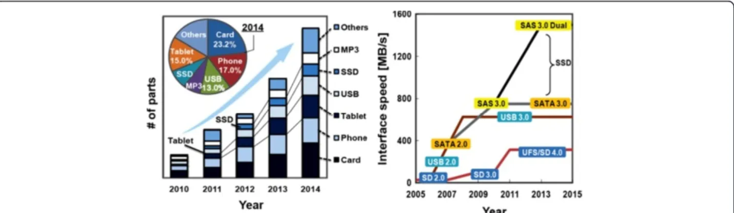
Successive creation of new mobile devices leads to the continual growth of NAND products as shown in Figure 4. To meet this market demand, early this year, 30-nm node technologies are in ramping-up phase, 20-30-nm node technologies are in the phase of transition to mass production, and a 10-nm node technology is under de-velopment. In addition, the future market requires high-speed operation even up to approximately 1,500 MB/s in order to satisfy a large amount of data correspondence [37]. However, high-speed operations cause high power consumption and chip temperature increase, which can deteriorate NAND reliability. Hence, reduction of ope-rating voltage is inevitable to achieve the future NAND. Opportunities for the use of 3-D as well as polymer mem-ory design in modern electronic circuits are rapidly expanding, based on the very high performance and unique functionality. However, their practical implementa-tion in electronic applicaimplementa-tions will ultimately be decided by the ability to produce devices and circuits at a cost that is significantly below that needed to manufacture conven-tional electronic circuits based on, for example, silicon. If successful, these low-cost fabrication processes will ultim-ately result in the printing of large-area organic electronic circuits on a sheet of plastic paper using a roll-to-roll method, where low-temperature deposition of organics is followed by metal deposition and patterning in a continu-ous, high-speed process analogcontinu-ous, perhaps, to processes used in the printing of documents or fabrics.
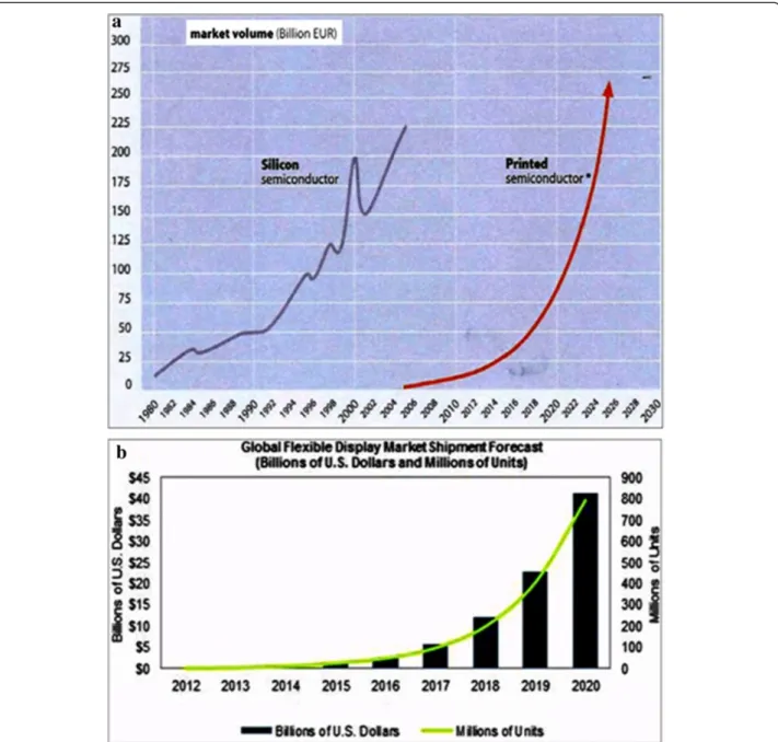
In recent years, IDTechEx finds that the total market for printed, flexible, and organic electronics will grow from $16.04 billion in 2013 to $76.79 billion in 2023 and this growing trend is expected to continue in the coming years (see Figure 5a). The majority of that is OLEDs (only organic, not printed) and conductive ink used for a wide range of applications. On the other hand, stretch-able electronics, logic and memory, and thin-film sen-sors are much smaller ingredients but having huge growth potential as they emerge from R&D [38]. The re-port specifically addresses the big picture that over 3,000 organizations are pursuing printed, organic, flexible elec-tronics, including printing, elecelec-tronics, materials, and packaging companies. While some of these technologies are in use now - indeed there are main sectors of busi-ness which have created billion-dollar markets - others are commercially embryonic.
Another key potential market for printed/flexible elec-tronics is next-generation transparent conductive film to replace brittle and expensive indium tin oxide (ITO) in touch screens and displays, lighting, and photovoltaics. Touch display research says that the market for non-ITO transparent conductors will be about $206 million this year and grow to some $4 billion by 2020 as shown in Figure 5b. ‘High demand for touchscreens for notebook and PC size displays has created a shortage of ITO touch sensors since the end of last year to drive more interest in these tech-nologies, and the more flexible and potentially cheaper re-placement technologies are getting more mature, notes Jennifer Colegrove, president and analyst, who will speak at the FlexTech workshop on transparent conductors. She notes that Atmel, Fujifilm, Unipixel and Cambrios are all in some phase of production’ [39]. A large amount of the semiconductor market (approximately 20%) is given by the semiconductor memories; thus, the market for chips will develop in the next few years. This study reports that there is an analysis of the production process and the subsequent value chain, which comprises a benchmark analysis of the main segments of the semiconductor industry.
Recently, the 3-D nonvolatile memory structure has also attracted considerable attention due to its potential to re-place conventional Flash memory in next-generation NVM applications [37,40]. 3-D memories are gathering increasing attention as future ultra-high-density memory technologies to keep a trend of increasing bit density and reducing bit cost. The NAND Flash market is continu-ously growing by the successive introduction of innovative devices and applications. To meet the market trend, 3-D NVMs are expected to replace the planar one, especially for 10-nm nodes and beyond. Therefore, the fundamentals and current status of the 3-D NAND Flash memory are reviewed and future directions are discussed [41]. 3-D
integration promises to be an excellent replacement of current technologies for the development of NAND Flash memory. Time is running out for planar NAND technol-ogy. It will not be long that planar NAND will be com-pletely replaced by 3-D NAND. 3-D NAND promises to satisfy the growing need of NAND memory [37].
Finally, NVM technologies have a bright future since every end-use application needs to store some parame-ters or some amount of an application program in the on-board NVM to enable it to function. The upcoming NVMs are the big hope for a semiconductor memory market, which provides memories for systems to run with flexibility, reliability, high performance, and low
power consumption in a tiny footprint in nearly every electronic application. Recent market trends have indi-cated that commercialized or near-commercialized cir-cuits are optimized across speed, density, power efficiency, and manufacturability. Flash memory is not suited to all applications, having its own problems with random-access time, bit alterability, and write cycles. With the increasing need to lower power consumption with zero-power standby systems, observers are predicting that the time has come for alternative technologies to capture at least some share in specific markets such as automotive smart airbags, high-end mobile phones, and RFID tags. An embedded nonvolatile memory with superior perform-ance to Flash could see widespread adoption in system-on-chip (SoC) applications such as smart cards and microcontrollers.
Emerging NVM technologies for applications
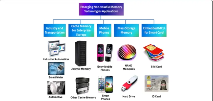
The new emerging nonvolatile random-access memory products address the urgent need in some specific and small-form devices. Therefore, iRAP felt a need to do a detailed technology update and market analysis in this industry [42]. Recently, Yole Développement reports de-scribe that emerging memory technologies have great potential to improve future memory devices to be in-creasingly used in various markets of industry and trans-portation, enterprise storage, mobile phones, mass storage, and smart cards [43]. Emerging NVM applica-tions in various markets are shown in Figure 6. But there are numerous opportunities existing for novel architec-tures and applications that these emerging memory technologies can enable. These new emerging NVM
products address the urgent need in some specific and small-form devices. Therefore, emerging nonvolatile memory products provide market data about the size of growth of the application segments and the developments of business opportunities. Until now, only FeRAM, PCM, and MRAM were industrially produced and available in low-density chips to only a few players. Thus, the market was quite limited and considerably smaller than the vola-tile DRAM- and nonvolavola-tile Flash NAND-dominant mar-kets (which enjoyed combined revenues of $50+ billion in 2012). However, in the next 5 years, the scalability and chip density of those memories will be greatly improved and will spark many new applications with NVM market drivers explained in more detail.
Accompanied by the adoption of STT-MRAM and PCM cache memory, enterprise storage will be the lar-gest emerging NVM market. NVM will greatly improve the input/output performance of enterprise storage sys-tems whose requirements will intensify with the growing need for web-based data supported by floating mass servers. In addition, mobile phones will increase their adoption of PCM as a substitute to Flash NOR memory in MCP packages to 1-gigabyte (GB) chips made avail-able by Micron in 2012. Higher-density chips, expected in 2015, will allow access to smart phone applications that are quickly replacing entry-level phones. STT-MRAM is expected to replace SRAM in SoC applica-tions, thanks to lower power consumption and better scalability. Smart cards and microcontrollers (MCU) will likely adopt MRAM/STT-MRAM and PCM as a substi-tute to embed Flash. Indeed, Flash memory cell size re-duction is limited in the future. The NVM could reduce
the cell size by 50% and thus be more cost-competitive. Additional features like increased security, lower power consumption, and higher endurance are also appealing NVM attributes. The mass storage markets served by Flash NAND could begin using 3-D RRAM in 2017 to 2018, when 3-D NAND will slow down its scalability as predicted by all of the main memory players. If this hap-pens, then a massive RRAM ramp-up will commence in the next decade that will replace NAND; conditional 3-D RRAM cost-competitiveness and chip density are available. It is expected surely that the emerging NVM business will be very dynamic over the next 5 years, thanks to improvements in scalability/cost and density of emerging NVM chips [44].
According to a recently published report from Yole Développement, Emerging Non-volatile Memory Tech-nologies, Industry Trends and Market Analysis, the global
market for emerging nonvolatile random-access memory products was projected to have reached $200 million in 2012. This market is expected to increase to $2,500 million by 2018 at an average annual growth at a CAGR of +46% through the forecast period with mobile phones, smart cards, and enterprise storage as main growth drivers (Figure 7). Market adoption of memory is strongly dependent on its scalability. This Yole Développement re-port provides a precise memory roadmap in terms of technological nodes, cell size, and chip density for each emerging NVM such as FeRAM, MRAM/STT-MRAM, PCM, and RRAM. A market forecast is provided for each technology by application, units, revenues, and also market growth as given a detailed account of emerging NVM mar-ket forecast (Figure 7). PCM devices, the densest NVM in 2012 at 1 GB, will reach 8 GB by 2018, which are expected to replace NOR Flash memory in mobile phones and will
also be used as a storage class memory in enterprise stor-age. MRAM/STT-MRAM chips will reach 8 to 16 GB in 2018. They will be widely sold as a storage class memory and possibly as a DRAM successor in enterprise storage after 2018. By 2018, MRAM/STT-MRAM and PCM will surely be the top two NVM on the market. Combined, they will represent a $1.6 billion business by 2018, and their sales will almost double each year, with double-density chips launched every 2 years. FeRAM will be more stable in terms of scalability, with 8- to 16-MB chips available by 2018; the development of a new FRAM material could raise scalability, but we do not expect it to be widely indus-trialized and commercialized before 2018. FeRAM will grow at a steady growth rate (10% per year) and will focus on industrial and transportation applications because of the low-density availability, whereas RRAM revenues would not really surge by 2018, with the availability of high-density chips of several tens of gigabytes that could replace NAND technology. Meanwhile, it has also been considered by memory technologist experts that for large-volume markets like mass storage NAND, only one tech-nology will be adopted in order to reduce production cost and RRAM seems to be the best candidate. But the real massive adoption of emerging NVM as a replacement for NAND and DRAM will happen after 2020.
Advances in Flash memory technologies
Flash memory is basically a MOSFET nonvolatile device that can be electrically erased and reprogrammed [3,45]. It is a technology that is primarily used in memory cards and Flash drives for general storage and transfer of data between computers and other digital products. Since the invention of the transistor, NVSM had been the most important invention in the electron device field. The floating gate memory was used to store the information and a tunneling current for programming and erasing operations. The charge is injected into or removed from the floating gate and the floating gate remains in that state, even after power is removed, which means that Flash memory is nonvolatile. The invention of NVSM further gave rise to a new class of memory devices and hence broadened its applications to become ubiquitous. There are a large number of products in the market now which use Flash devices exclusively as secondary storage. Few examples of their applications include medical diag-nostic systems, notebook computers, digital audio players, digital cameras, mobile phones, personal digital assistants, digital televisions, universal serial bus (USB) Flash per-sonal disks, Global Positioning Systems, and many more. Semiconductor storage devices store data in tiny memory cells made of very small transistors and capacitors made of semiconductor materials such as silicon. Each cell can hold 1 bit of information and an array of cells stores a large chunk of information. Flash devices are gaining
popularity over conventional secondary storage devices like hard disks. The Flash memory fabrication process is compatible with the current CMOS process and is a suit-able solution for embedded memory applications. A Flash memory cell is simply a MOSFET cell, except that a poly-silicon floating gate [46] (or a poly-silicon nitride charge trap layer) is sandwiched between a tunnel oxide and an inter-polyoxide to form a charge storage layer [47]. Although Flash memory is likely the standard charge storage device for the next generation, scaling may eventually be limited by the tunnel oxide limit [8]. In terms of the operation speed of program and erase, Flash memory requires a thin tunnel oxide to enhance the carrier transport between the floating gate and the silicon substrate. However, the very thin tunnel oxide suffers from many reliability issues like reduction in operation voltage, and after a considerable number of program and erase cycles, the tunnel oxide undergoes deterioration loss [48]. Thus, researchers have focused on possible solutions and proposed alternate tech-nologies, including nitride-based memory, nanocrystal memory, and switching memory. All other nonvolatile memories require integration of new materials that are not as compatible as the conventional CMOS process. NOR and NAND Flash memory technologies
NOR and NAND Flash, two major Flash types, are dom-inant in the memory market. NOR Flash has lower dens-ity but a random-access interface, while NAND Flash has higher density and interface access through a com-mand sequence [49]. Their corresponding structures are shown in Figure 8. NOR and NAND Flash come from the structure used for the interconnections between memory cells. Intel is the first company to introduce a commercial (NOR type) Flash chip in 1988, and Toshiba released the world's first NAND Flash in 1989 [50]. De-pending on how the cells are organized in the matrix, it is possible to distinguish between NAND Flash memor-ies and NOR Flash memormemor-ies. In NOR Flash, cells are connected in parallel to the bit lines, which notably allow the cells to be read and programmed individually. The parallel connection of NOR Flash cells resemble the parallel connection of transistors in a CMOS NOR gate architecture. On the other hand, in NAND Flash, the cells are connected in series, resembling a NAND gate. The series connections consume less space than the par-allel ones, reducing the cost of NAND Flash. It does not, by itself, prevent NAND cells from being read and pro-grammed individually. Most of the engineers and scien-tists are not so familiar with the differences between these two technologies. Generally, they usually refer to the NOR architecture as ‘Flash’ and are unaware of the NAND Flash technology and its many benefits over NOR [51]. This could be due to the fact that most Flash devices are used to store and run codes (usually small),
for which NOR Flash is the default choice, although we are providing some major differences between NOR and NAND Flash technologies by their architecture and the internal characteristic features of the individual Flash.
NOR Flash is slower in erase operation and write op-eration compared to NAND Flash [52]. This means that NAND Flash has faster erase and write times. Moreover, NAND Flash has smaller erase units, so fewer erases are needed. NOR Flash can read data slightly faster than NAND Flash. NOR Flash offers complete address and data buses to randomly access any of its memory loca-tions (addressable to every byte). This makes it a suitable replacement for older ROM BIOS/firmware chips, which rarely needs to be updated. Its endurance is 10,000 to 1,000,000 erase cycles. NOR Flash is highly suitable for storing codes in embedded systems. Most of today's microcontrollers come with built-in Flash memory [53].
NAND Flash occupies a smaller chip area per cell. This makes NAND Flash available in greater storage densities and at lower costs per bit than NOR Flash. It also has up to ten times the endurance of NOR Flash. NAND is more fit as storage media for large files includ-ing video and audio. USB thumb drives, SD cards, and MMC cards are of NAND type [54]. NAND's advantages are fast write (program) and erase operations, while NOR's advantages are random access and byte write capability. NOR's random access ability allows for exe-cute in place (XiP) capability, which is often a require-ment in embedded applications. NAND is slow random accessible, while NOR is hampered by having slow write and erase performance. NAND is better suited for filing
applications. However, more processors include a direct NAND interface and can boot directly from NAND (without NOR). However, NAND cannot perform read and write operations simultaneously; it can accomplish these at a system level using a method called shadowing, which has been used on PCs for years by loading the BIOS from the slower ROM into the high-speed RAM.
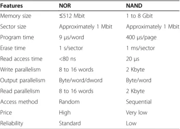
Table 1 highlights the major differences between NOR and NAND. It shows that NAND is ideal for high-capacity data storage while NOR is best used for code storage and execution, usually in small capacities. There are many other differences between these two technolo-gies which will be further discussed individually. How-ever, those listed in the table are enough to strongly differentiate the types of applications using them: NOR is typically used for code storage and execution. This, mainly in capacities up to 4 MB, is common in applica-tions such as simple consumer appliances, low-end cell phones, and embedded applications, while raw NAND is used for data storage in applications such as MP3 players, digital cameras, and memory cards [55-57]. The codes for raw NAND-based applications are stored in NOR devices.
Scaling and challenges of Flash memory technologies Currently, there have been increasing demands on redu-cing the feature size in microelectronic products and more interest in the development of Flash memory de-vices to meet the growing worldwide demand. A conven-tional FG memory device must have a tunnel oxide layer thickness of 8 nm to prevent charge loss and to make 10 years' data retention certain. This necessity will limit scalability for Flash memory devices [8,58]. Thus, in order to meet technology scaling in the field of memory and data storage devices, mainstream transistor-based Flash technologies will be developed gradually to incorp-orate material and structural innovations [59]. Dielectric
Figure 8 Comparison of NOR Flash array and NAND Flash array architectures.
Table 1 Comparison between NOR and NAND Flash memories [55-57]
Features NOR NAND
Memory size ≤512 Mbit 1 to 8 Gbit
Sector size Approximately 1 Mbit Approximately 1 Mbit Program time 9μs/word 400μs/page Erase time 1 s/sector 1 ms/sector Read access time <80 ns 20μs Write parallelism 8 to 16 words 2 Kbyte Output parallelism Byte/word/dword Byte/word Read parallelism 8 to 16 words 2 Kbyte Access method Random Sequential
Price High Very low
scaling in nonvolatile memories has been reached near to the point where new approaches will be required to meet the scaling requirements while simultaneously meeting the reliability and performance requirements for future products. High-dielectric-constant materials are being explored as possible candidates to replace both the traditional SiO2and oxide/nitride/oxide (ONO) films
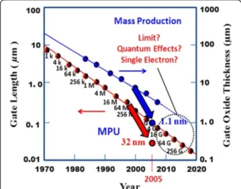
used in Flash memory cells. Flash cell scaling has been demonstrated to be really possible and to be able to fol-low Moore's law down to the 90-nm technology genera-tions. The technology development and the consolidated know-how are expected to sustain the scaling trend down to the 50-nm technology node and below as fore-casted by the International Technology Roadmap for Semiconductors (ITRS) in Figure 9, which indicates that the silicon MOSFET was already in the nanoscale. The minimum feature size of an individual CMOSFET has shrunk to 15 nm with an equivalent gate oxide thickness (EOT) of 0.8 nm in 2001 [13]. However, semiconductor Flash memory scaling is far behind CMOS logic device scaling. For example, the EOT of the gate stack in semi-conductor Flash memory is still more than 10 nm. Moreover, semiconductor Flash memory still requires operation voltages of more than 10 V, which is still far from the operation voltage of CMOS logic devices. It is important to scale the EOT of the gate stack to achieve a small memory cell size and also prolong battery life.
Another limitation of FG technology is that tunnel oxide scaling is limited by stress-induced leakage current (SILC) related to charge transfer problem as indicated in Figure 10 [60,61]. The SILK increases with decreasing oxide thickness. This can be attributed to tunneling assisted by the traps in the bulk of the dielectric. Trap-assisted tunneling can take place at very low electric fields. If the density of traps is increased, the leakage will
also increase. Electrical stress can increase the number of these traps. So it becomes an important limitation of scaling down the memory device [62]. For EOT < 8 nm, a single oxide trap will cause to complete the charge loss in the FG Flash cell. The scaling of the gate stacks and operation voltages are often related to each other. A tun-nel oxide thickness of more than 8 nm is currently used in the commercial Flash memory chip to meet the 10 years' data retention time requirement. If the tunnel oxide were to be scaled below 2 nm, the operation volt-age could be reduced from more than 10 V to below 4 V [63]. Unfortunately, the retention time would also be re-duced, from 10 years to several seconds. This physical damage to the tunnel oxide during the cycling process causes data retention problems, program disturbance, read disturbance, and erratic characteristic behavior of the FG memory cell. Such problems severely limit the reliability and multilevel cell operation. This basic limita-tion of the tunnel oxide thickness becomes increasingly important with scaling. New storage node concepts are also becoming attractive as an alternative approach to address some of the dielectric scaling limitations. Flash memory adopts a charge stored in a silicon nitride as the trapping layer, which exhibits significantly reduced defect-related leakage current and very low SILC as compared to SiO2with a similar EOT [64]. Such a
relent-less reduction of device dimensions has many challenges like retention, endurance, reduction in the number of elec-trons in the FG, dielectric leakage, cell-to-cell cross talk, threshold voltage shift, and reduction in memory window margins [65,66]. The key concept of real scaling issues such as material and structural changes in Flash memory technologies is provided in detail in the next distinct part. FG Flash memory technology
The FGNV memory is a basic building block of Flash memory, which is based on FG thin-film storage (TFS) memories that have been developed with the addition of an erase gate configuration. The conventional FG mem-ory (Figure 11a) consists of a MOSFET configuration that is modified to include polysilicon as a charge stor-age layer surrounded by an insulated inner gate (floating gate) and an external gate (control gate). This what makes Flash memory nonvolatile and all floating gate memories to have the same generic cell structure. Charge is trans-ferred to or from the floating gate through a thin (8 to 10 nm) oxide [1,67]. Because the floating gate is electric-ally isolated by the oxide layer, any electrons placed on it are trapped there. Flash memory works by adding (char-ging) or removing (dischar(char-ging) electrons to and from a floating gate. A bit's 0 or 1 state depends upon whether or not the floating gate is charged or discharged. When elec-trons are present on the floating gate, current cannot flow through the transistor and the bit state is ‘0’. This is the
Figure 9 The trend of MOSFET scaling from ITRS. Reproduced from ITRS Corp.
normal state for a floating gate. When electrons are re-moved from the floating gate, current is allowed to flow and the bit state is‘1’. The FG memory has achieved high density, good program/erase speed, good reliability, and low operating voltage and promotes endurance for Flash memory application.
SONOS memory technology
In order to solve the scaling issue of the FG memory, the SONOS memory has been proposed as a Flash technology since the 1980s [68,69]. The acronym SONOS is derived from the structure of the device as shown in Figure 11b. The SONOS device is basically a MOSFET, where the gate has been replaced by an ONO dielectric. The SONOS memory has a better charge retention than the FG memory when the FG bit
cell's tunneling oxide layer is below 10 nm [70]. More-over, the SONOS memory exhibits many advantages, e.g., easy to fabricate, high program/erase (P/E) speed, low pro-gramming voltage and power consumption, and better po-tential for scalability below the 70-nm node, according to the ITRS [71]. The charge, holes or electrons, are injected into the nitride layer using direct tunneling through the tunnel oxide layer. The nitride layer is electrically isolated from the surrounding transistor, although charges stored on the nitride directly affect the conductivity of the under-lying transistor channel. Since the SONOS memory pos-sesses spatially isolated deep-level traps, a single defect in the tunneling oxide will not cause discharge of the mem-ory cell. The thickness of the top oxide is important to prevent the Fowler-Nordheim tunneling of electrons from the gate during erase. When the polysilicon control gate is
Figure 10 Schematic plots of a Flash memory cell and the degradation of its tunnel oxide. The degradation leads to the formation of percolation paths responsible for the FG charge loss, hence the loss of the stored information. The presence of traps in the energy barrier yields the trap-assisted tunneling mechanism and originates the stress-induced leakage current (SILC).
Figure 11 Schematics of the conventional FG memory and SONOS. Schematics of (a) floating gate and thin-film storage-based embedded nonvolatile memory bit cells, depending on the charge stored inside the gate dielectric of a MOSFET, and (b) the nitride traps (SONOS), embedded into the gate oxide of a MOSFET.
biased positively, electrons from the transistor source and drain regions tunnel through the oxide layer and get trapped in the silicon nitride. This results in an energy barrier between the drain and the source, raising the threshold voltage Vth (the gate-source voltage necessary
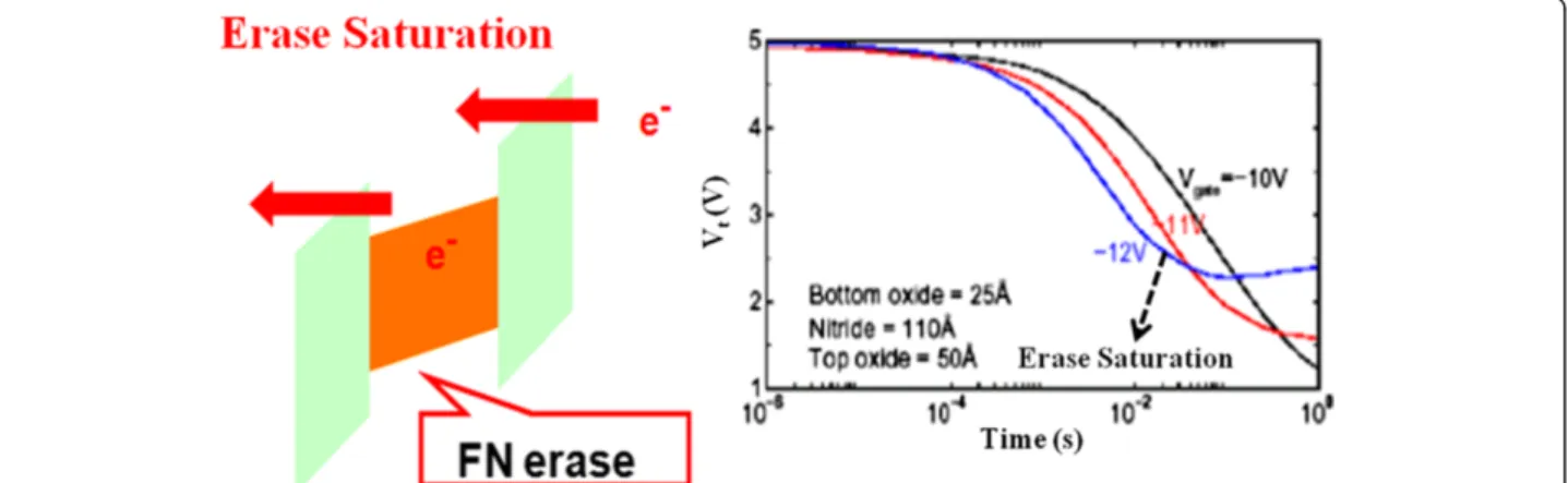
for current to flow through the transistor). Moreover, the nitride layer is electrically isolated from the surrounding transistor, although charges stored on the nitride directly affect the conductivity of the underlying transistor chan-nel. The oxide/nitride sandwich typically consists of a 2-nm-thick oxide lower layer, a 5-2-nm-thick silicon nitride middle layer, and a 5- to 10-nm-thick oxide upper layer [72,73]. However, SONOS-type Flash memories have sev-eral drawbacks such as shallow trap energy level, erase sat-uration, and vertical stored charge migration [74]. The programming speed and operating voltage problems can be solved by reducing the tunnel oxide thickness. At low tunnel oxide thickness, the issues that impact SONOS-type memories include erase saturation and vertical charge migration, which seriously degrade the retention capability of the memory [75]. Thus, many concerns still remain for the SONOS type of memories, which will be discussed in the next section.
Limitations of FG and SONOS memory technologies
Scaling demands very thin gate insulators in order to keep short channel effects and control the shrinkage of the device size and maximize the performance. When the tunneling oxide thickness is below 10 nm, the stor-aged charge in the FG is easy to leak due to a defect in the tunneling oxide formed by repeated write/erase cy-cles or direct tunneling current.
The tunneling gate oxide thickness in a conventional Flash memory cannot be scaled down to sub-7 nm be-cause of charge retention [76]. The SONOS Flash mem-ory can relieve the problem but still has a relatively thick gate dielectric thickness of about 7 nm. Therefore, con-ventional SONOS Flash memory also has a scaling-down
problem. Many studies have shown that the charge reten-tion characteristics in scaled SONOS nonvolatile memory devices with a low gate oxide thickness and at high temperature are problematic with shallow-level traps [48,77,78]. For the conventional SONOS memory, erase saturation and vertical stored charge migration [79,80] are the two major drawbacks; the most challenging tasks are how to maintain an acceptable charge capability of the discrete storage nodes and how to fabricate nanocrystals with constant size, high density, and uniform distributions [81]. When the trap energy level is shallow, erase satur-ation and vertical migrsatur-ation occur and the electron charge decay rate increases due to low tunnel oxide thickness, issues that impact SONOS-type memories as shown in Figure 12. This erase saturation makes SONOS erase less as the erase voltage or the tunnel oxide thickness is increased. Since the SONOS memory uses silicon ni-tride as a charge trapping layer, the electrons in the Si sub-conduction band will tunnel through the tunneling oxide and a portion of the nitride, and this conse-quently degrades the program speed. Besides this, the conduction band offset of nitride is only 1.05 eV and back-tunneling of the trapped electron may also occur. Although applying a very high electric field may accel-erate the de-trapping rate, the gate electron injection current exceeds the de-trapping but resulting in prac-tically an increase in charge and no erasing. Using an ultra-thin (<2 nm) tunnel oxide offers an efficient charge direct tunneling erase and opens a memory win-dow. However, the direct tunneling cannot be turned off at a low electric field, leading to poor retention and read disturb. Thus, the SONOS memory cannot be used for NAND Flash without further innovation of new memory technologies. The main reason for the growth of emerging NVM technologies is that scaling has now become a serious issue for the memory indus-try. Not only are many of these new technologies inher-ently more scalable, but also they seem well suited to
Figure 12 Fowler-Nordheim (FN) tunneling of electrons from the gate during erase and erase saturation in SONOS nonvolatile memory. This indicates the reduced memory window as the erase voltage is increased. Reproduced from ref. [74].
the next generation of mobile computing and commu-nications that will demand high-capacity memories capable of storing and rapidly accessing video and a large database without overburdening battery power sources.
Many alternate device structures are proposed to hopefully circumvent these scaling challenges and to im-prove the device performance. In an effort to continue Moore's law and overcome the ultimate limitations of MOS-based memory devices, other storage concepts have been proposed in search of the ‘unified memory’. The ideal memory device or the so-called‘unified mem-ory’ would satisfy simultaneously three requirements: high speed, high density, and nonvolatility. At the present time, such an ideal memory has not been devel-oped. FGNVSM has high density and nonvolatility, but its P/E speed is low. DRAM has high speed (approxi-mately 10 ns) and relatively high density, but it is vola-tile. SRAM has very high speed (approximately 5 ns), but it suffers from very low density and volatility. Many nonvolatile memory devices have been proposed on the basis of changing charge storage materials and new de-vice concepts for the‘unified memory’. These structures will be considered in the next sections. In light of such issues, emerging memory solutions seem to be a key technology.
Current emerging memory technologies
Recent studies have revealed that there is a close correl-ation among existing and emerging memory technolo-gies in view of scalability. The scaling trend of memory transition leads to smaller and smaller memory devices, which have been routinely observed. To further support this assertion, another set of current progress in memory technology is described to the increasing importance of memory to users' experience and the importance of memory to system performance. There are many emer-ging memory technologies which are trying to replace existing memory technologies in the market. These new memory devices such as RRAM, PCM, and STT-RAM have read/write/retention/endurance characteristics dif-ferent from those of conventional SRAM, DRAM, and Flash [82]. But the ideal characteristics of new emerging memory technologies have to be meeting the perform-ance of SRAM and the density of NAND Flash in terms of stability, scalability, and switching speed. Thus, going beyond the traditional bistable memory, the possibilities of multilevel, high-performance memory devices suitable for market must be explored. Currently, there are several technologies that show some promise; some of these new emerging technologies are MRAM, FeRAM, PCM, STT-RAM, nano-random-access memory (NRAM), race-track memory, RRAM and memristor, molecular mem-ory, and many others [10,83]. Each of these memory
technologies will be briefly outlined and discussed in the following sections. In view of the commercial production, currently, MRAM, FeRAM, and PCM are in commercial production but still remain limited to niche applications relative to DRAM and NAND Flash. There is a prospect that among the emerging memory technologies, MRAM, STT-RAM, and RRAM are the most promising ones, but they are still many years away from competing for indus-try adoption [84]. It is necessary for any new technology to be able to deliver most for industry adoption. For in-dustry adoption on a mass scale, some parameters must be matched with existing memory technologies. In consid-eration of new technology for industry application, the scalability of the technology, speed of the device, power consumption to be better than existing memories, endur-ance, densities, better than existing technologies and most importantly the cost; if the emerging technology can only run one or two of these attributes, then, at most desirable, it is likely to be resigned to niche applications.
MRAM
MRAM or magnetic RAM is a nonvolatile RAM tech-nology under development since the 1990s. RRAM methods of storing data bits use magnetic charges in-stead of the electrical charges used by DRAM and SRAM technologies. MRAM, first developed by IBM in the 1970s [85], is expected to replace DRAM as the memory standard in electronics. MRAM is basically based on memory cells having two magnetic storage ele-ments, one with a fixed magnetic polarity and another with a switchable polarity. These magnetic elements are positioned on top of each other but separated by a thin insulating tunnel barrier as shown in the cell structure in Figure 13. Moreover, scientists define a metal as mag-netoresistive if it shows a slight change in electrical re-sistance when placed in a magnetic field. By combining the high speed of static RAM and the high density of DRAM, proponents say that MRAM could be used to
significantly improve electronic products by storing greater amounts of data, enabling it to be accessed faster while consuming less battery power than existing elec-tronic memories. Technically, it works with the state of the cell, which is sensed by measuring the electrical resist-ance while passing a current through the cell. Because of the magnetic tunnel effect [86], if both magnetic moments are parallel to each other, then the electrons will be able to tunnel and the cell is in the low resistance ‘ON’ state. However, if the magnetic moments are antiparallel, the cell resistance will be high. The memory characteristics of MRAM of writing and erasing are fulfilled by passing a current through the write line to induce a magnetic field across the cell. MRAM has been slowly getting off the ground but has now entered the market and will become increasingly available for mass production in the couple of years and beyond. Currently, it has reached some level of commercial success in niche applications [87]. Various companies such as Samsung, IBM, Hitachi and Toshiba, and TSMC are actively developing variant technologies of MRAM chips. In view of power consumption and speed, MRAM competes favorably than other existing memories such as DRAM and Flash, with an access time of a few nanoseconds [88-90]. Although it has some limitation during the‘write’ operation, the smaller cell size could be limited by the spread of the magnetic field into neighbor-ing cells and need an amendment to compete completely as a universal memory. The price of MRAM is also an-other issue and considered a limiting factor, with prices far in excess of all the currently established memories at approximately £2 to £3 ($3 to $5) per megabyte [91]. Ac-cording to this price level, MRAM is in excess of 1,000 times the price of Flash memory and over 10,000 times the price of hard disk drives. It is expected that of the next-generation memory technologies, MRAM, in the fu-ture, will have the biggest market, followed by FeRAM, PCRAM, and memristors.
STT-MRAM
STT-MRAM is a magnetic memory technology that exerts the base platform established by an existing memory called MRAM to enable a scalable nonvolatile memory so-lution for advanced process nodes [92,93]. It is a new kind of magnetic RAM with the following features: fast read and write times, small cell sizes, potentially even smaller, and compatibility with existing DRAM and SRAM. As we have discussed in the previous section, MRAM stores data according to the magnetization direction of each bit and the nanoscopic magnetic fields set the bits in con-ventional MRAM. On the other hand, STT-MRAM uses spin-polarized currents, enabling smaller and less energy-consuming bits. The basic cell structure of STT-RAM is depicted in Figure 14. In addition, STT-STT-RAM writing is a technology in which an electric current is
polarized by aligning the spin direction of the electrons flowing through a magnetic tunnel junction (MTJ) element. Data writing is performed by using the spin-polarized current to change the magnetic orientation of the information storage layer in the MTJ element [94]. The resultant resistance difference of the MTJ element is used for information readout. STT-RAM is a more appropriate technology for future MRAM produced using ultra-fine processes and can be efficiently embed-ded in subsequent generations of such semiconductor devices as FPGAs, microprocessors, microcontrollers, and SoC. A special bonus for embedded designers is the fact that the internal voltage STT-RAM requires is only 1.2 V. The difference between STT-MRAM and a conventional MRAM is only in the writing operation mechanism; the read system is the same. The memory cell of STT-MRAM is composed of a transistor, an MTJ, a word line (WL), a bit line (BL), and a source line (SL) [95]. Currently, STT-RAM is being developed in companies including Everspin, Grandis, Hynix, IBM, Samsung, TDK, and Toshiba. However, for STT-RAM to be adopted as a universal mainstream semiconductor memory, some key challenges should be resolved: the simultaneous achievement of low switching current and high thermal stability. It must be dense (approximately 10 F2), fast (below 10 ns of read and write speeds), and operating at low power [96].
FeRAM
FeRAM is a nonvolatile RAM that combines the fast read and write access of DRAM cells, consisting of a capacitor and transistor structure as shown in Figure 15. The cell is then accessed via the transistor, which en-ables the ferroelectric state of the capacitor dielectric to be sensed. In spite of its name, FeRAM does not contain iron. The polarization properties of a ferroelectric sub-stance are used as a memory device. Today's FeRAM uses lead zirconate titanate (PZT); other materials are being considered. The main developer of FeRAM is
Ramtron International. FeRAM is the most common kind of personal computer memory with the ability to retain data when power is turned off as do other nonvol-atile memory devices such as ROM and Flash memory [97]. In a DRAM cell, the data periodically need refresh-ing due to the dischargrefresh-ing of the capacitor, whereas FeRAM maintains the data without any external power supply. It achieves this by using a ferroelectric material in the place of a conventional dielectric material be-tween the plates of the capacitor. When an electric field is applied across dielectric or ferroelectric materials, it will polarize, and while that field is removed, it will depolarize. But the ferroelectric material exhibits hyster-esis in a plot of polarization versus electric field, and it will retain its polarization. One disadvantage of FeRAM is that has a destructive read cycle. The read method in-volves writing a bit to each cell; if the state of the cell changes, then a small current pulse is detected by indi-cating that the cell was in the OFF state. However, it is a fast memory that can endure a high number of cycles (e.g., 1014) [98], meaning that the requirement for a write cycle for every read cycle will not result in short product lives with a very low power requirement. It is expected to have many applications in small consumer devices such as personal digital assistants (PDAs), handheld phones, power meters, and smart cards, and in security systems. FeRAM is faster than Flash mem-ory. It is also expected to replace EEPROM and SRAM for some applications and to become a key component in future wireless products. Even after FeRAM has achieved a level of commercial success, with the first devices released in 1993 [99,100], current FeRAM chips offer performance that is either comparable to or ex-ceeding current Flash memories [98,101], but still slower than DRAM.
PCRAM
PCRAM, also known as PCM, perfect RAM (PRAM), OUM, and chalcogenide RAM (CRAM), is a type of nonvolatile RAM based on a class of material called chalcogenide glasses that can exist in two different phase states (e.g., crystalline and amorphous) [102,103]. The basic PCRAM cell structure is depicted in Figure 16. Most phase-change materials contain at least one elem-ent from group 6 of the periodic table, and the choice of available materials can be further widened by doping these materials [104-107]. In particular, the most prom-ising are the GeSbTe alloys which follow a pseudobinary composition (between GeTe and Sb2Te3), referred to as
GST. These materials are in fact commonly used as the data layer in rewritable compact disks and digital versa-tile disks (CD-RW and DVD-RW) where the change in optical properties is exploited to store data. The struc-ture of the material can change rapidly back and forth between amorphous and crystalline on a microscopic
Figure 15 Basic structure of a FeRAM cell. The crystal structure of a ferroelectric and an electric polarization-electric field hysteresis curve are also shown.
Figure 16 Basic PCRAM cell structure. Reproduced from IBM-Macronix-Qimonda.
scale. The material has low electrical resistance in the crystalline or ordered phase and high electrical resist-ance in the amorphous or disordered phase. This allows electrical currents to be switched ON and OFF, repre-senting digital high and low states. This process has been demonstrated to be on the order of a few tens of nanoseconds [108], which potentially makes it compat-ible with Flash for the read operation, but several orders of magnitude faster for the write cycle. This makes it possible for PCM to function many times faster than conventional Flash memory while using less power. In addition, PCM technology has the potential to provide inexpensive, high-speed, high-density, high-volume non-volatile storage on an unprecedented scale. The physical structure is three-dimensional, maximizing the number of transistors that can exist in a chip of fixed size. PCM is sometimes called perfect RAM because data can be overwritten without having to erase it first. Possible problems facing PCRAM concern the high current dens-ity needed to erase the memory; however, as cell sizes decrease, the current needed will also decrease. PCM chips are expected to last several times as long as cur-rently available Flash memory chips and may prove cheaper for mass production. Working prototypes of PCM chips have been tested by IBM, Infineon, Samsung, Macronix, and others. Also, the production of PCM has been announced recently by both collaborations between Intel and STMicroelectronics as well as with Samsung [109,110].
Comparison of primary contenders for MRAM, STT-RAM, FeRAM, and PCM technologies
Before going to other emerging memories, we herein pro-vide a comparison among MRAM, FeRAM, and PCM. The specific features of these memory devices are pro-vided in Table 2. Relatively mature, new-material memor-ies such as MRAM, STT-RAM, FeRAM, and PCM can offer a variety of features that have potential to be the can-didates for next-generation nonvolatile memory devices.
Brand-new concepts such as RRAM, molecular, organic/ polymer, and other nanowire-based memory technologies have also been proposed. These are discussed in detail in the following section.
RRAM
RRAM is a disruptive technology that can revolutionize the performance of products in many areas, from con-sumer electronics and personal computers to automo-tive, medical, military, and space. Among all the current memory technologies, RRAM is attracting much atten-tion since it is compatible with the convenatten-tional semi-conductor processes. Memristor-based RRAM is one of the most promising emerging memory technologies and has the potential of being a universal memory technol-ogy [111]. It offers the potential for a cheap, simple memory that could compete across the whole spectrum of digital memories, from low-cost, low-performance ap-plications up to universal memories capable of replacing all current market-leading technologies, such as hard disk drives, random-access memories, and Flash memor-ies [112]. RRAM is a simple, two-terminal metal-insulator-metal (MIM) bistable device as shown in the basic configuration in Figure 17. It can exist in two dis-tinct conductivity states, with each state being induced by applying different voltages across the device termi-nals. RRAM uses materials that can be switched between two or more distinct resistance states. Many companies are investing metal oxide nanolayers switched by voltage pulses. Researchers generally think that the pulses' elec-tric fields produce conducting filaments through the in-sulating oxide. HP Labs plans to release prototype chips this year based on‘memristors’ in which migrating oxygen atoms change resistance [113]. Xu et al. have also defined that among all the technology candidates, RRAM is con-sidered to be the most promising as it operates faster than PCRAM and it has a simpler and smaller cell structure than magnetic memories (e.g., MRAM or STT-RAM) [114]. In contrast to a conventional MOS-accessed Table 2 Summary of primary contenders for MRAM, FeRAM, STT-RAM, and PCM technologies
Features FeRAM MRAM STT-RAM PCM
Cell size (F2) Large, approximately 40 to 20 Large, approximately 25 Small, approximately 6 to 20 Small, approximately 8 Storage mechanism Permanent polarization of a
ferroelectric material (PZT or SBT)
Permanent magnetization of a ferromagnetic material in a MTJ
Spin-polarized current applies torque on the magnetic moment
Amorphous/polycrystal phases of chalcogenide alloy
Read time (ns) 20 to 80 3 to 20 2 to 20 20 to 50
Write/erase time (ns) 50/50 3 to 20 2 to 20 20/30
Endurance 1012 >1015 >1016 1012
Write power Mid Mid to high Low Low
Nonvolatility Yes Yes Yes Yes
Maturity Limited production Test chips Test chips Test chips Applications Low density Low density High density High density