One-step fabrication and
field emission properties of petal-like carbon nanotubes
Tsung-Chi Hung
a,⁎
, Chia-Fu Chen
b,⁎
, Wha-Tzong Whang
aa
Department of Materials Science and Engineering, National Chiao Tung University, Hsinchu 30050, Taiwan b
Department of Materials Science and Engineering, Ming Dao University, Chang Hua 52345, Taiwan
a b s t r a c t
a r t i c l e i n f o
Available online 7 November 2008 Keywords:Carbon nanotube Nanoflake Carbon dioxide Field emission
We have used bias-assisted microwave plasma chemical vapor deposition to synthesize (i) carbon nanotubes (CNTs) possessing a graphitic carbon nanoflake (CNF) morphology, (ii) CNF spheres, and (iii) a pure carbon nanoflake film (CNFF) on stainless-steel substrates. We employed CH4and CO2as the precursors to these carbon nanomaterials (CNMs); the use of CO2aided the destruction of the CNT surfaces and reduced the growth temperature range to 380–450 °C at 300 W, as a result of the presence of oxygen-based species in the plasma. Applying an external bias of−150 V led to the growth of CNTs possessing specifically oriented graphitic CNFs. We used scanning electron microscopy and high-resolution transmission electron microscopy to observe the morphologies and graphitic structures of these CNMs. Field emission measurements of a CNT/CNF-coated electrode revealed that the turn-onfield was ca. 2.73 V/μm.
© 2008 Elsevier B.V. All rights reserved.
1. Introduction
Since the discovery of C60 in 1985[1], nanometer-sized carbon materials have attracted much attention because of their large specific surface-to-volume ratios, high electrical conductivities [2–4], and their potential for application in energy storage, electronic, and display devices[5–8]. A variety of nanostructures, including carbon nanotubes (CNTs) and carbon nanoflakes (CNFs), have been developed by several groups[9,10]. Among the carbon nanostructures, we are interested in the preparation and properties of carbon nanowalls possessing graphite structures, sharp edges, and, in particular, large specific surface-to-volume ratios. Lee et al. reported a two-step process [including bias-assistedfilament chemical vapor deposition (CVD) at 550 °C] for the formation of CNTs possessing nanoflake morphologies[11]. This novel structure has attracted much attention recently, especially because of its field emission properties. In a previous study, we developed a two-step process for attaching CNFs to the walls of CNTs in a H2/CH4system at a high substrate temperature (ca. 700 °C)[12]. The use of a pre-deposited catalyst for the subsequent growth of the nanoflakes was essential. In this present study, we developed a simpler process, requiring lower growth temperatures, to obtain novel structures for particular applications, especially coldfield emission.
Herein, we describe a one-step process, using a bias-assisted microwave plasma chemical vapor deposition (MPCVD) system, for the fabrication of CNTs decorated by CNFs on stainless steel. Using CO2 and CH4as reactant gases provided morphologies that differed from
those obtained using the H2/CH4 system. We investigated the influence of the external negative bias on the resulting structures and examined thefield emission performance of the CNTs decorated with CNFs.
2. Experimental details
Stainless-steel plates (type 316A; thickness: 0.2 mm) having an area of 1 × 1 cm2served as the substrates for the support of the carbon nanomaterials (CNMs). The substrates were cleaned sequentially with acetone and methanol in an ultrasonication bath, rinsed with
⁎ Corresponding authors.
E-mail addresses:[email protected](T.-C. Hung),[email protected]
(C.-F. Chen). Fig. 1. SEM image of stainless steel after H2plasma pretreatment for 10 min.
0925-9635/$– see front matter © 2008 Elsevier B.V. All rights reserved. doi:10.1016/j.diamond.2008.10.050
Contents lists available atScienceDirect
Diamond & Related Materials
deionized water, and then dried with nitrogen gas. Prior to deposition, plasma pre-treatment was performed in the MPCVD system at a H2 flow rate of 40 sccm, a gas pressure of 10 Torr, and a power of 300 W. The reactant gas, a mixture of CH4and CO2(3:2), was then introduced into the reaction chamber and the main growth of the CNMs was performed for 30 min. The working pressure and power were maintained at 10 Torr and 300 W, respectively. The applied bias was 0,−100, or −150 V. The substrate temperature was measured using an optical pyrometer and thermocouple placed in direct contact with the substrate holder.
The morphologies and structures of the carbon-based electrodes were investigated using a JEOL JSM 6700 scanning electron micro-scope (SEM) and a JEOL JEM 4000 high-resolution transmission electron microscope (HRTEM).
3. Results and discussion
In general, catalyst particles are essential for the successful synthesis of structural carbon materials, especially when using CVD systems. Thus, we pretreated our stainless-steel substrates with H2
Fig. 2. Carbon nanomaterials prepared after performing bias-assisted MPCVD for 30 min: (a, b) pure CNFFs formed in the absence of an applied external bias; (c, d) CNFSs formed at an external applied bias of−100 V; (e, f) CNTs/CNFs formed at an external applied bias of −150 V.
plasma for 10 min to provide metallic particles to act as catalysts for the growth of CNMs; fromFig. 1we estimate that their sizes ranged from 100 to 150 nm. Under the plasma deposition conditions, we obtained three different kinds of CNM structures when applying three different negative bias to the substrate. Fig. 2(a) and (b) displays magnified images of the pure carbon nanoflake film (CNFF) obtained at a bias of 0 V. Each CNF had a width of ca. 1μm and a thickness of ca. 5 nm. The substrate temperature, as measured by a thermocouple placed on the back side of the substrate, was low (ca. 380 °C). The formation of afilm of CNFs aligned perpendicular to the substrate
surface occurs as a result of the intrinsic self-potential around surface
[13]. When we applied a bias of −100 V to the substrate, carbon nanoflake spheres (CNFSs) having diameters of ca. 2 μm formed on the substrate [Fig. 2(c) and (d)]. We suspect that they arose primarily through a process of damaging, but not breaking, the surfaces of the catalyst particles (i.e., forming many defects, such as cracks) and then precipitating carbon at those sites. The mechanism follows the carbon dissociation, diffusion, and precipitation model, which describes the growth and structures of carbon materials[14,15], providing a sphere covered radially withflakes. In this model, the hydrocarbon adsorbs
dissociatively to supply carbon atoms to the particle surface; the surface carbon undergoes dissociation, diffuses through the particle along interstitial lattice planes, and precipitates from corresponding sites at opposite facets. The diffusion is driven by a concentration gradient. If the size of the metallic particle acting as the catalyst exceeds the carbon diffusion length, the process leads preferentially to the formation of CNFs to CNTs[16,17]. Based on considerations of the surface energy, it has been suggested that anisotropic deposition occurs during the growth of pure CNFs; the self-potential established on the substrate surface causes vertical growth because thefield lines are invariably terminated normal to the surface[18,19].
When we increased external bias to−150 V, we obtained a quite different morphology: a novel structure comprising CNTs decorated by CNFs (CNTs/CNFs) [Fig. 2(e) and (f)]. The substrate temperature was ca. 450 °C. The diameters of the CNTs decorated by nanoflakes ranged from ca. 100 nm to slightly less than 1 µm. We suspect that the breaking of catalysts, caused by the bias of−150 V, was beneficial to the formation of CNTs with smaller iron particles captured inside them. By comparison to H2/CH4system, introducing CO2dramatically reduces the growth temperature because of its effect on the ionization energy. Oxygen-containing species, such as O–H[20,21], can effec-tively remove amorphous carbon and even graphitic structures from the surfaces of CNTs, especially with the assistance provided by an applied bias. We suspect that the nanotubes were attacked by the accelerated oxygen-containing ions; the resulting damaged CNT surface would exhibit many tiny substructural features presenting free carbon atoms (dangling bonds) while the CNTs remained growing. The damaged, rough surfaces of the CNTs contain many active sites for the aggregation of carbon atoms. Collisions between these aggregated carbon atoms would lead to the formation of horn-like structures that would later turn into walls of nanoflakes, as predicted by molecular dynamics simulations[22]. Of course, the resulting CNFs would also be attacked during this process to leave numerous active sites for the further formation and attachment of additional CNFs.Fig. 1(f) reveals many spots distributed on the CNTs and CNFs. We suspect that the spots are active sites at which future CNFs would grow. Finally, the substrate is covered with interlaced CNTs presenting a nanoflake morphology.
Fig. 3presents TEM images of related CNF/CNT structures.Fig. 3(a) displays the tubular structure of a multiwall CNT that is decorated in places by nanoflakes;Fig. 3(b) provides a magnified image of the CNT wall, revealing the high degrees of graphitization on both sides. We estimate the distance between the two graphite layers to be ca. 0.35 nm, very close to the theoretical value (0.34 nm).Fig. 3(c) displays the structure of a CNT covered entirely by CNFs, which are also
attached to other nanoflakes. This morphology is consistent with that determined from SEM images.Fig. 3(d) and (e) presents the top and side views, respectively, of a CNF/CNT; both reveal graphitic structures having thicknesses ranging from 5 to 20 nm. The enormous number of CNFs that are stacked onto the CNT inFig. 3(c) suggests that further continuous growth of CNFs can arise through a process of carbon deposition and collision.Fig. 4(a) and (b) displays the early and late stages, respectively, of the growth of a CNF.Fig. 4(a) reveals that the structure of the CNF was very disordered and small in size at the onset of CNF growth. This disordered CNF continues to grow through collisions of carbon atoms to form graphitic, ordered layers [Fig. 4(b)]. Furthermore, these images suggest that the CNFs arise directly from the CNTs because of the similarity between the graphitic layer distance in the CNTs and the CNFs. Using an electron energy loss spectroscopy system mounted on the TEM equipment, we detected no elements other than carbon atoms at the CNF–CNT interface, suggesting that the attachment of CNFs to CNTs is a catalyst-free process.
For practical applications, we were interested in using the CNT/CNF surface as an electrode because of its special morphology. Indeed, the CNT/CNFs have great potential for use infield emission applications.
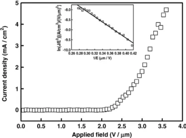
Fig. 5displays the emission current density (J, A/cm2) plotted with respect to the applied electricfield (E, V/μm). The competitive turn-on field (ET) was ca. 2.73 V/μm, corresponding to 1 mA/cm2
. We attribute this performance to the edge-emission characteristics being enhanced
Fig. 4. TEM images of a CNF attached to a CNT at the (a) beginning and (b) end of the formation process.
by the graphitic structure of the CNTs and to the good connection between the CNFs and the CNTs. The inset to Fig. 5A provides a corresponding Fowler–Nordheim (F–N) plot for the CNT/CNF surface. The straight line having a negative slope in the high field region reveals that thefield emission from the CNT/CNF structure follows the traditionalfield emission (F–N) model.
4. Conclusion
Bias-assisted MPCVD allows pure CNFFs, CNFSs, and CNTs presenting graphitic CNFs to be synthesized on stainless-steel substrates. The applied bias has a significant influence on the type of CNM structures formed on the stainless-steel substrate. The one-step fabrication of the CNT/CNF structures occurred when using CO2/ CH4plasma at an external bias of−150 V. The process occurred at a relatively low temperature (b450 °C) because the presence of oxygen-based species in the plasma was beneficial to the destruction of the CNT surfaces to create lattice-matched sites for the formation of the nanoflakes. In an examination of the field emission properties, we observed a low turn-onfield for the CNT/CNF system (ca. 2.73 V/μm) because of the graphitic structures of its CNMs and, more importantly, the sharp edges of the nanoflakes. On the basis of their simple, low-temperature fabrication and great emission properties, we believe that CNTs presenting graphitic CNFs are promising candidate materials for use in cold cathode display devices.
Acknowledgments
We gratefully thank Ragor Lao for assistance with HRTEM at National Chiao Tung University, and National Science Council of Taiwan forfinancial support under grant no. NSC 95-2221-E-451-011.
References
[1] H.W. Kroto, J.R. Heath, S.C. O'Brien, R.F. Curl, R.E. Smalley, Nature 318 (1985) 162. [2] T.M. Whitney, J.S. Jiang, P.C. Searson, C.L. Chien, Science 261 (1993) 1316. [3] M.M.J. Treacy, T.W. Ebbenson, J.M. Gibson, Nature 381 (1996) 678. [4] P. Delaney, H.J. Choi, J. Ihm, S.G. Louie, M.L. Cohen, Nature 391 (1998) 466. [5] S.S. Wong, E. Joselevich, A.T. Woolley, C.L. Cheung, C.M. Lieber, Nature 394 (1998) 52. [6] S.J. Tans, A.R.M. Verschueren, C. Dekker, Nature 393 (1998) 49.
[7] C. Liu, Y.Y. Fan, M. Liu, H.T. Cong, H.M. Cheng, M.S. Dresselhaus, Science 286 (1999) 1127. [8] S. Fan, M.G. Chapline, N.R. Franklin, T.W. Tombler, A.M. Cassel, H. Dai, Science 283
(1999) 512.
[9] D. Gournis, M.A. Karakassides, T. Bakas, N. Boukos, D. Petridis, Carbon, 40 (2002) 2641. [10] G.H. Chen, W.G. Weng, D. J Wu, C. L Wu, J.R. Lu, P.P. Wang, X.F. Chen, Carbon 42
(2004) 753.
[11] N.G. Shang, C.P. Li, W.K. Wong, C.S. Lee, I. Bello, S.T. Lee, Appl. Phys. Lett. 81 (2002) 5024. [12] C.C. Chen, C.F. Chen, I. H Lee, C.L. Lin, Diamond Relat. Mater. 14 (2005) 1897. [13] C. Bower, W. Zhu, S. Jin, O. Zhou, Appl. Phys. Lett. 77 (2000) 830.
[14] S.B. Sinnott, R. Andrews, D. Quian, A.M. Rao, Z. Mao, E.C. Dickey, F. Derbyshire, Chem. Phys. Lett. 315 (1999) 25.
[15] N.M. Rodriguez, A. Chambers, R.T.K. Baker, Langmuir 11 (1995) 3862.
[16] M. Yudasaka, R. Kikuchi, Y. Ohki, E. Ota, S. Yoshimura, Appl. Phys. Lett. 70 (1997) 1817. [17] S.K. Srivastava, A.K. Shukla, V.D. Vankar, V. Kumar, Thin Solid Films 492 (2005) 124. [18] B. Chapman, Glow Discharge Process, Wiley, New York, 1980.
[19] Y. Wu, B. Yang, Nano Letters 2 (2002) 355.
[20] M. Chen, C.M. Chen, L.K. Wu, J. Mater. Sci. 37 (2002) 3561.
[21] H. Chatei, M. Belmahi, M.B. Assouar, L. Le Brizoual, P. Bourson, J. Bougdira, Diamond Relat. Mater. 15 (2006) 1041.