A Comprehensive Study of Inversion Current in MOS
Tunneling Diodes
C.-H. Lin, B.-C. Hsu, M. H. Lee, and C. W. Liu, Senior Member, IEEE
Abstract—The gate current of MOS tunneling diodes biased at inversion region with different substrate doping is investigated. For p-type substrate (1–5 -cm) devices, the tunneling diode works in the deep depletion region and the inversion current is dominated by the thermal generation rate of minority electrons via traps at Si/SiO2 interface and in the deep depletion region. The activation energy is approximately equal to half of the silicon bandgap independent of gate voltage. For devices on p+substrate (0.01–0.05-cm), the band-to-traps tunneling and band-to-band tunneling are the dominating current components at inversion bias, and reveal a strong field dependence and a weak tempera-ture dependence. The band-to-traps and band-to-band current components are even more significant in the devices on the p++ substrate (0.001–0.0025-cm). Finally, the effects of temperature and light illumination on inversion current of MOS tunneling diodes will be also discussed.
Index Terms—Inversion current, MOS tunneling diode, ultra-thin oxide.
I. INTRODUCTION
F
OR future deep-submicron ULSI technology, it is expected that the SiO gate dielectric will be less than 3 nm for a technology node beyond 0.13 m [1]. The gate current becomes significant for MOS diodes with such ultrathin oxide. This gate current has been utilized for many novel applications, such as light-emitting diodes (LEDs) [2], [3], and photodetectors [4], although the significant gate current is a problematic issue in ULSI circuits. Due to the capability of carrier supply from the source and drain, the gate currents biased at accumulation re-gion and at inversion rere-gion have similar behaviors in MOS-FETs [5]. While, due to the lack of carrier supply, the inver-sion current is quite different from the accumulation current for MOS tunneling diode. The mechanisms of accumulation cur-rent of the MOS tunneling diodes have been extensively studied [6]–[8]. The mechanism of inversion current is not yet well un-derstood in the MOS diodes, although this inversion current of MOS diodes on heavily doped substrate is similar to gate-in-duced drain leakage current (GIDL) [9], [10]. Recently, GhettiManuscript received December 27, 2000; revised April 17, 2001. This work was supported by the National Science Council, Taiwan, R.O.C. (89-2218-E-002-017, and 89-2218-E-002-012). The review of this paper was arranged by Editor K. Najafz.
C. W. Liu is with the Department of Electrical Engineering, National Taiwan University, Taipei, Taiwan, R.O.C., and also with the Graduate Institute of Electronics Engineering, National Taiwan University, Taipei, Taiwan, R.O.C. (e-mail: [email protected]).
C.-H. Lin, B.-C. Hsu, and M. H. Lee are with the Department of Electrical Engineering, National Taiwan University, Taipei, Taiwan, R.O.C. (e-mail: [email protected]; [email protected]; [email protected]).
Publisher Item Identifier S 0018-9383(01)06896-4.
et al. investigated the inversion current of MOS diodes with
thick oxide ( 6 nm) based on tunneling mechanisms [11]. A theoretical model including band-to-band tunneling, interface state tunneling, carrier generation through the interface, carrier generation in the depletion region, and diffusion current have been reported [12]. For ultrathin oxide ( 3 nm), the carrier tunneling rate through oxide is sufficient large, and the carrier generation rate is the bottleneck for current transport. In this paper, we demonstrate that three carrier-generation mechanisms are responsible for the inversion current of NMOS tunneling diodes. The mechanisms are Shockley-Read-Hall (SRH) gener-ation, band-to-band tunneling, and band-to-traps tunneling. The doping level of substrate determined the dominant mechanism.
II. EXPERIMENT
The ultrathin gate oxide of the NMOS diode was grown by rapid thermal oxidation (RTO) on p-type silicon (100) substrate with three different doping levels, 1–5 -cm (labeled as “p”), 0.01–0.05 -cm (p ), and 0.001–0.025 -cm (p ). The gas flows were 500 sccm nitrogen and 500 sccm oxygen at reduced pressure. Before the growth of RTO oxide, the sample was cleaned by a HF dip and in-situ hydrogen bake at 1000 C for 2 min. After the growth of the ultrathin gate oxide, the sample was in-situ annealed in hydrogen and nitrogen for 10 min each at 900 C. The oxide thickness was measured by ellipsometry. NMOS diodes had Al gate electrodes with various circular areas defined by photolithography. The temperature dependence of current-voltage ( ) characteristic was performed on a low-leakage hot chuck. Device temperature was set using the hot chuck before the measurements were conducted. The photocurrent and its temperature dependence are also measured by using metal halide lamp and the hot chuck.
III. CARRIERGENERATIONMODELS
The inversion tunneling current was simulated by a self-coded program method based on the conventional SRH model, band-to-traps tunneling model, and band-to-band tun-neling model. The band profile was determined by conventional Poisson’s equation.
A. Shockley–Read–Hall (SRH) Model
For the MOS devices with oxide thickness less than 3 nm, the tunneling rate of the minority carrier through the oxide is sufficiently effective at large gate bias. Therefore, the current is dominated by the minority carrier generation rate via traps at 0018–9383/01$10.00 © 2001 IEEE
Si/SiO interface and in the deep depletion region. The conven-tional SRH recombination model, which determines the gener-ation rate of electron-hole pairs, can be described by [13]
(1)
(2) where
thermal velocity;
and state densities of the conduction band and the valance band, respectively;
intrinsic carrier density; trap energy level;
and capture cross sections of the traps for electrons and holes, respectively;
and electron and hole densities, respectively; and lifetime times of electron and hole, respectively. The inversion current from SRH mechanism is deter-mined by the integration of the thermal generation rate over the whole deep depletion region and interface states energy level, which is given by
(3)
where
width of the deep depletion region;
thermal generation rate of electrons in deep depletion region;
thermal generation rate of electrons via interface states with the assumption that is uniformly distributed in the bandgap.
Only one trap level is considered in the depletion region during the calculation of the electron generation rate in the depletion region.
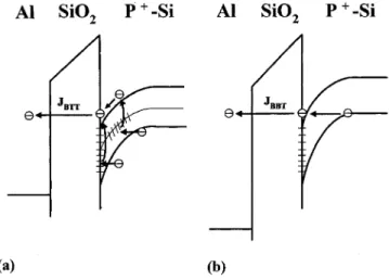
B. Band-to-Traps Tunneling Model
For p and p substrate devices, owing to high doping concentration, which causes the shrinkage of the depletion re-gion width, the band-to-traps (bulk traps and interface states) tunneling and band-to-band tunneling become the dominated mechanisms of the inversion current. At small gate bias, the band-to-traps tunneling model dominates the tunneling current due to small silicon surface bending ( 1.1 eV), as shown in Fig. 1(a). However, when gate bias is large enough to have sur-face band bending larger than 1.1 eV, the band-to-band tun-neling [Fig. 1(b)] becomes more significant than band-to-traps tunneling. Both the models have voltage dependence on the tun-neling current, while the previous SRH model of devices on p substrates has a relatively weak voltage dependence. Hurkx et
al. have proposed a modified recombination model which
in-cludes both hole tunneling and electron tunneling in heavily
Fig. 1. Schematic band diagram of current transport mechanisms: (a) band-to-traps (bulk traps and interface states) tunneling and (b) band-to-band tunneling.
doped gated-diodes [14], [15], and the generation rate of elec-trons via traps is given by
(4) where is the conventional SRH generation rate, and
is given by
(5) with
(6) where is the local electric field of silicon, and the is the effective mass of carriers. Some electrons tunnel from valance band to the most active bulk traps in the depletion region (lo-cated near the middle of bandgap), jump up to conduction band, and then tunnel to Al electrode. Some electrons near the Si/SiO interface will tunnel from valance band to interface states di-rectly, instead of tunneling to bulk traps. For the weak electric field, i.e., V/cm at room temperature, is much less than 1, and (4) will reduce back to the conventional SRH model [13]. Therefore, the band-to-traps tunneling current is given by
(7) On the right-hand side, the first integration term represents the component of band-to-bulk traps tunneling, and the second term represents the component of band-to-interface trap tunneling. There is no position integral in the second term, since there is one-to-one correspondence between interface trap energy and the position from which the electrons tunnel.
C. Band-to-Band Tunneling Model
As gate bias larger than 2 V, the band-to-band tunneling starts to dominate the inversion tunneling current. In MOS tunneling diodes with heavily doped substrate, the carrier transport
TABLE I
LIST OF THEPARAMETERSUSED INSIMULATION
mechanism is similar to that of GIDL in MOSFET, which is attributed to band-to-band tunneling near the gate-to-drain overlap region. Wu et al. have proposed a new quasi-two-di-mensional (quasi-2-D) model for band-to-band tunneling current [16]. Neglecting the lateral electric field effect, the band-to-band tunneling current can be attained by inte-grating the tunneling rate through the whole depletion region, and is given by
(8) where tunneling rate can be described as
(9) where
silicon bandgap;
electric field in the depletion region; electron effective mass.
Therefore, the band-to-band tunneling current is strongly depen-dent on electric field. The bandgap dependence on temperature is used to simulate the temperature dependence of band-to-band tunneling current. The silicon bandgap is given by [17]
(10) where
; ; for silicon.
Silicon bandgap decreases at high temperature, and thus, the band-to-band tunneling current increases as temperature increases.
The parameters of SRH, band-to-traps tunneling, and band-to-band tunneling models used in the simulation are listed in Table I.
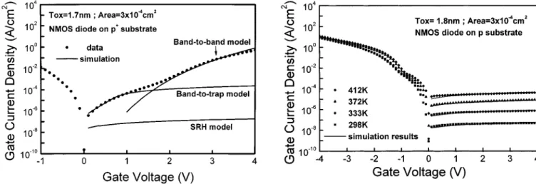
Fig. 2. I0V curve of an NMOS diode on p substrate with SRH simulation results.
IV. COMPARISON OFSIMULATIONS ANDEXPERIMENTAL RESULTS
Fig. 2 shows the curve of an Al/1.8 nm oxide/p-Si diode with an area of cm . The simulated inversion tun-neling current based on SRH model agrees well with the mea-sured curve, and the inversion current is relatively constant in log scale. For ultrathin oxide device, the tunneling rate is con-trolled by the oxide voltage, which causes the direct tunneling of electrons from silicon to Al electrode. In NMOS tunneling diode, as positive gate bias increases, the oxide voltage increases very slightly, and most gate voltage drops on silicon with the formation of deep depletion region [4]. Therefore, the tunneling current is limited by the thermal generation rate of electrons in deep depletion region and at Si/SiO interface, and can be sim-ulated by conventional SRH generation/recombination model.
The curve of an Al/1.7 nm oxide/p -Si diode with an area of cm is shown in Fig. 3. There is an enormous disparity with the previous device on p substrate. The tunneling current re-veals strong field dependence and a kink around 1.7 V, indicating the transition between band-to-traps tunneling and band-to-band
Fig. 3. I0V curve of an NMOS diode on p substrate with SRH, band-to-traps tunneling, and band-to-band tunneling simulation results.
Fig. 4. I0V curve of an NMOS diode on p substrate with simulation results.
tunneling. At positive gate bias smaller than 1.7 V, the generation rate of electrons is dominated by electrons tunneling from valance band to traps (bulk traps and interface traps), and then jumping up to conduction band. However, when gate bias is larger than 1.7 V (the surface band bending is larger than the bandgap), the generation of electrons is mainly due to electron tunneling from valance band to conduction band directly. The simulation results of band-to-traps tunneling and band-to-band tunneling give an ex-cellent fit to the experimental data. For comparison, the SRH com-ponent is also shown in Fig. 3 and is negligible, as compared to the other two components.
Fig. 4 shows the curve of an Al/1.3 nm oxide/p -Si diode with an area of cm . The gate tunneling current increases abruptly at V, which is due to the turn-on of band-to-band tunneling mechanism (surface bending 1.12 eV). The larger inversion tunneling current level than that of the device on p substrate is the result of large electric field in the device on p substrate. The higher substrate doping concentra-tion, which makes tunneling rate larger, leads to larger band-to-band tunneling current. The simulation results are also shown in Fig. 4. Due to the measurement limit ( 100 mA), the experimental data points with current larger than 100 mA are not
Fig. 5. I0V curves of an NMOS diode on p substrate at different temperatures with SRH simulation results.
shown in Fig. 4. The heavy doping magnifies the band-to-traps and band-to-band tunneling.
V. TEMPERATURE ANDILLUMINATIONEFFECT ONINVERSION CURRENT
A. Temperature Effect
Fig. 5 shows the curves of an Al/1.8 nm oxide/p-Si diode with an area of cm at different temperatures (room temperature to 412 K). At positive gate bias, the gate cur-rent is relatively constant in log scale and reveals strong temper-ature dependence with activation energies of 640 meV at bias voltage from 0.5 3 V. This confirms that the gate tunneling cur-rent is limited by the thermal generation rate of electron-hole pairs via defect at Si/SiO interface and in the deep depletion region. The temperature dependence of gate current is different from previous work, reported by Yassine et al. [18], where the gate inversion current shows weaker temperature effect at high gate voltage on thicker oxide (3.7 nm). Note that at the low neg-ative gate bias ( V V), however, the gate tunneling current exhibit weaker temperature dependence with activation energy of 155 meV at 0.5 V (not shown in Fig. 7), which may be caused by electron tunneling from Al gate electrode to sil-icon through interface states [19].
The curves of an Al/1.7 nm oxide/p -Si diode with an area of cm from room temperature to 410 K are shown in Fig. 6. The inversion current of the device with heavily doped p substrate exhibits strong field dependence at all measurement temperatures. The band-to-traps tunneling current has stronger temperature dependence as compared to the band-to-band tun-neling current. This is due to temperature dependence of the SRH function in the band-to-traps transport equation.
The activation energies of the devices on p and p substrates at different gate voltages are extracted from Figs. 5 and 6 and are given in Fig. 7. For the devices on p-type substrate, the activation energy reveals no field dependence and its value is approximately equal to half of the silicon bandgap, since the most active traps are located in the middle of the bandgap. The SRH model can also describe the thermal generation rate of electron-hole pairs in the deep depletion and at Si/SiO interface at elevated temperature.
Fig. 6. I0V curves of an NMOS diode on p substrate at different temperatures with simulation results.
Fig. 7. Extraction of the activation energy at various gate voltage for p and p substrate devices.
On the contrary, for the devices on p substrate, the activa-tion energy exhibits strong field dependence. At high gate bias ( V), the band-to-band tunneling current shows very small temperature dependence with an activation energy of 50 meV. At low gate bias ( V), the band-to-traps tunneling current has the activation energy of 290 meV.
B. Illumination Effect
Fig. 8 shows the dark current and photocurrent of an Al/2.3 nm oxide/p-Si tunneling diode at different illumination den-sities, and the device area is cm . The photocur-rent was excited by metal halide lamp with a spectrum sim-ilar to sun. The dark and photocurrent are relatively constant in log scale for positive gate bias larger than 0.2 V. For p sub-strate device, however, due to compete with the band-to-band tunneling current, the photocurrent can only observed signifi-cantly at small gate bias ( V) under the applied light intensity (Fig. 9). Photo excitation generates much more elec-trons than thermal generation alone, and therefore the SRH and band-to-traps regimes have a measurable increase in tunneling current. However, even with photo excitation, the band-to-band tunneling current is still dominant under high band bending con-ditions, and independent of the light intensity.
Fig. 8. Dark and photo currents of an NMOS tunneling diode on p substrate.
Fig. 9. Dark and photo currents of an NMOS tunneling diode on p substrate.
Fig. 10. Activation energies of an NMOS diode on p substrate at different illumination densities.
Fig. 10 shows the illumination density dependence of the ac-tivation energy in p-type substrate devices biased at low gate voltage (0.5 V) extracted from the measurement at dif-ferent temperatures and light exposure density (not shown here). Under the illumination, most excess electrons are generated in conduction band by the photo excitation, which is independent of temperature. The inversion current consists of the
thermal-generated current due to temperature as well as the photo-gen-erated current due to the photo illumination. The photo-gener-ated current is dependent on the illumination intensity and has no temperature dependence. Therefore, the temperature depen-dence becomes less significant when the illumination intensity increases. This is shown in Fig. 10 and the activation energies of inversion current with no light exposure, 6.9 mW/cm expo-sure, and 21.4 mW/cm exposure are 640 meV, 210 meV, and 136 meV, respectively. However, the detailed modeling, which can predicted the activation energy under the photo excitation using the SHR model, is still under investigation.
VI. CONCLUSION
In conclusion, the comprehensive study of gate inversion current in MOS tunneling diodes with different substrate doping is investigated. For p-type substrate devices, the inversion tunneling current is dominated by the thermal generation rate of electron-hole pairs via interface traps and the traps in the deep depletion region. The inversion current is relatively constant in log scale and shows strong temperature and illumination density dependence. The value of activation energy is approximately equal to half of the silicon bandgap, since the most active traps are located near the middle of the bandgap. On the contrary, for p and p substrate devices, the gate current is dominated by band-to-band tunneling at high gate bias and by band-to-traps tunneling at low gate bias. The gate current of the device on p substrate biased at inversion region exhibits stronger field dependence and weaker temperature dependence than devices on p substrate.
REFERENCES
[1] International Technology Roadmap for Semiconductors, 1999. [2] C. W. Liu, M. H. Lee, M.-J. Chen, I. C. Lin, and C.-F. Lin,
“Room-tem-perature electroluminescence from electron-hole plasmas in the metal oxide silicon tunneling diodes,” Appl. Phys. Lett., vol. 76, no. 12, pp. 1516–1518, 2000.
[3] C. W. Liu, M. H. Lee, M. J. Chen, C.-F. Lin, and M. Y. Chern, “Rough-ness-enhanced electroluminescence from metal oxide silicon tunneling diodes,” IEEE Electron Device Lett., vol. 21, pp. 601–603, Dec. 2000. [4] C. W. Liu, W. T. Liu, M. H. Lee, W. S. Kuo, and B. C. Hsu, “A novel
photodetector using MOS tunneling structures,” IEEE Electron Device
Lett., vol. 21, pp. 307–309, June 2000.
[5] K. F. Schuegraf and C. Hu, “Low injection SiO breakdown model for very low voltage lifetime extrapoation,” IEEE Trans. Electron Devices, vol. 41, pp. 761–767, May 1994.
[6] A. Schenk and G. Heiser, “Modeling and simulation of tunneling through ultrathin dielectrics,” J. Appl. Phys., vol. 81, no. 12, pp. 7900–7908, 1997.
[7] N. Yang, W. K. Henson, J. R. Hauser, and J. J. Wortman, “Modeling study of ultrathin gate oxides using direct tunneling current and capac-itance-voltage measurements in MOS devices,” IEEE Trans. Electron
Devices, vol. 46, pp. 1464–1471, July 1999.
[8] L. F. Register, E. Rosenbaum, and K. Yang, “Analytic model for direct tunneling current in polycrystalline silicon-gate metal-oxide-semicon-ductor devices,” Appl. Phys. Lett., vol. 74, no. 3, pp. 457–459, 1999. [9] T.-E. Chang, C. Huang, and T. Wang, “Mechanisms of interface
trap-induced drain leakage current in off-state n-MOSFET’s,” IEEE Trans.
Electron Devices, vol. 42, pp. 738–743, Apr. 1995.
[10] M. Rosar, B. Leroy, and G. O. Schweeger, “A new model for the descrip-tion of gate voltage and temperature dependence of gate induced drain leakage (GIDL) in the low electric field region,” IEEE Trans. Electron
Devices, vol. 47, pp. 154–159, Jan. 2000.
[11] A. Ghetti, C.-T. Liu, M. Mastrapasqua, and E. Sangiorgi, “Characteriza-tion of tunneling current in ultrathin gate oxide,” Solid-State Electron., vol. 44, pp. 1523–1531, 2000.
[12] M. Y. Doghish and F. D. Ho, “A comprehensive analytical model for metal-insulator-semiconductor (MIS) devices,” IEEE Trans. Electron
Devices, vol. 39, pp. 2771–2780, Dec. 1992.
[13] A. S. Grove, Physics and Technology of Semiconductor Devices. New York: Wiley, 1967.
[14] G. A. M. Hurkx, D. B. M. Klaassen, and M. P. G. Knuvers, “A new recombination for devices simulation including tunneling,” IEEE Trans.
Electron Devices, vol. 39, pp. 331–338, Feb. 1992.
[15] G. A. M. Hurkx, H. C. de Graaff, W. J. Kloosterman, and M. P. G. Knu-vers, “A new analytical diode model including tunneling and avalanche breakdown,” IEEE Trans. Electron Devices, vol. 39, pp. 2090–2098, Sept. 1992.
[16] K.-F. You and C.-Y. Wu, “A new quasi-2-D model for hot-carrier band-to-band tunneling current,” IEEE Trans. Electron Devices, vol. 46, pp. 1174–1179, June 1999.
[17] S. M. Sze, Physics of Semiconductor Devices, 2nd ed. New York: Wiley, 1981.
[18] A. Yassine and R. Hijab, “Temperature dependence of gate current in ultrathin SiO in direct-tunneling regime,”, Integrated Reliability Work-shop Final Rep., pp. 56–61, 1997.
[19] A. Ghetti, E. Sangiorgi, J. Bude, T. W. Scorsch, and G. Weber, “Low voltage tunneling in ultrathin oxides: A monitor for interface states and degradation,” in IEDM Tech. Dig., 1999, pp. 731–734.
Chung-Hsun Lin received the B.S. and M.S.
degrees in electrical engineering in 1999 and 2001, respectively, from National Taiwan University, Taipei, Taiwan, R.O.C., where he is currently pursuing the Ph.D. degree in the Department of Electrical Engineering.
His current research interests include the improvement of reliability on MOS devices by deuterium incorporation, the mechanism of soft breakdown in MOS tunneling diodes, and the electrical characteristics of MOS devices.
Buo-Chin Hsu received the B.S. degree in 1999
from National Taiwan University, Taipei, Taiwan, R.O.C., where he is currently pursuing the Ph.D. degree in electrical engineering. His current research interests include the MOS tunneling photodetector, improvement of reliability on MOS devices by deuterium incorporation, the mechanism of soft breakdown in MOS tunneling diodes, and the electrical characteristics of MOS devices.
Min Hung Lee received the B.S. degree in physics
from National Chunghsin University, Taichun, Taiwan, R.O.C., in 1996, and the M.S. degree in physics from National Taiwan University (NTU), Taipei, Taiwan, in 1998. He is currently pursuing the Ph.D. degree in the Department of Electrical Engineering at NTU. His research interests include RTP equipment, RTCVD, and optical interconnects.
Chee Wee Liu (M’99–SM’00) received the B.S. and
M.S. degrees in electrical engineering from National Taiwan University (NTU), Taipei, Taiwan, R.O.C., in 1985 and 1987, respectively, and the Ph.D. degree in electrical engineering from Princeton University, Princeton, NJ, in 1994.
From 1994 to 1996, he was an Associate Professor at National Chunghsin University, Taichun, Taiwan. Now he is an Associate Professor at NTU. His current research interests include CMOS opto-electronics, optical interconnects, SiGe high-speed devices, and rapid thermal process. He invented the first MOS tunneling light-emitting diode and photodetector. He owns two patents on photodetectors.