Excitonic polaron and phonon assisted photoluminescence
of ZnO nanowires
Hsu-Cheng Hsu, Wen-Feng Hsieh*
Institute of Electro-Optical Engineering, National Chiao Tung University, 1001 Tahsueh Road, Hsinchu 30050, Taiwan, ROC Received 4 February 2004; received in revised form 22 May 2004; accepted 27 May 2004 by D.J. Lockwood
Available online 15 June 2004
Abstract
The coupling strength of the radiative transition of hexagonal ZnO nanowires to the longitudinal optic (LO) phonon polarization field is deduced from temperature dependent photoluminescence spectra. An excitonic polaron formation is discussed to explain why the interaction of free excitons with LO phonons in ZnO nanowires is much stronger than that of bound excitons with LO phonons. The strong exciton – phonon coupling in ZnO nanowires affects not only the Haung – Ray S factor but also the FXA-1LO phonon energy spacing, which can be explained by the excitonic polaron formation.
q2004 Elsevier Ltd. All rights reserved.
PACS: 73.61.Tm; 74.25.Gz; 78.55. 2 m
Keywords: A. Nanostructure; D. Optical properties; E. Photoluminescence
1. Introduction
One-dimensional (1D) semiconductor nanostructures, such as nanowires, have became important fundamental building blocks for nanophotonic devices and offer substantial promise for integrated nanosystems[1,2]. ZnO nanowires are especially interesting because they exhibit a large exciton binging energy (60 meV), a wide band gap (3.37 eV), and a lower lasing threshold, that are necessary critical elements of nanotechnologies. Recently, a number of investigations on the synthesis of ZnO nanowires have been reported[3 – 7]. Lasing behavior at room temperature, which is associated with well-oriented vertical self-assembled nanowires, has been demonstrated [8]. It is expected that the low lasing threshold is a result of highly efficient exciton emission due to the carrier confinement in 1D nanowires and the cavities that are naturally formed between the end faces of the aligned nanowires. It has also
great potential applications for short wavelength photonic devices. Despite such achievements, the understanding of the fundamental properties of ZnO nanowires is far from complete.
For strongly polar semiconductors, such as ZnO, an intense exciton – LO phonon interaction is expected accord-ing to Fro¨hlich polar intraband scatteraccord-ing and will induce phonon-assisted exciton emission accompanied by the exciton recombination [9 – 11]. Although exciton-related stimulated emission have been observed at room tempera-ture, which is attributed to the exciton – exciton scattering or the electron – hole plasma in the ZnO epitaxial films and ZnMgO multi-quantum wells (MQWs)[12 – 14], few studies addressed the low temperature and temperature-dependent excitonic luminescence of ZnO nanowires[15 – 17]. In this letter, we report the LO phonon-assisted luminescence of the neutral donor-bound excitons and the free excitons in the ZnO nanowires at various temperatures. We found that the energy separations between the phonon replica and their zero-order spectra exhibit unusual temperature dependence. An excitonic polaron model is used to explain these phenomena.
0038-1098/$ - see front matter q 2004 Elsevier Ltd. All rights reserved. doi:10.1016/j.ssc.2004.05.043
www.elsevier.com/locate/ssc
* Corresponding author. Tel.: þ886-3-57-121-21; ext. 56316; fax: þ 886-357-16-631.
2. Experimental
The growth of ZnO nanowires is based on the well-known vapor – liquid – solid (VLS) mechanism which is similar with that reported in Ref.[3]. A (0001) sapphire or alumina coated with a thin (around 10 nm) Au layer was put inside a quartz tube furnace. A powder mixture of pure ZnO (99.99%) and graphite (99.999%) was used as the starting materials and placed in an alumina boat. The boat was positioned in the center of the tube furnace and the substrate was placed 5 – 10 cm downstream of the mixed powder. The tube was evacuated to a pressure below 5 £ 1022Torr using a mechanical pump. The furnace temperature was increased to 900 8C at a rate of 50 8C/min and high-purity argon gas was then introduced into the quartz tube at a flow rate from 25 to 75 sccm during 4 – 8 h of growth. We observed a gray – white colored product on the surface of the Au-coated substrate and even on the wall of the tube close to the low-temperature end of the furnace.
The morphology and crystal structure of the nanowires were characterized by Scanning Electron Microscopy (SEM) and X-ray diffraction (XRD). The photolumines-cence measurement was made using 325 nm laser line of a 20 mw He – Cd laser and a TRIAX-320 spectrometer with a 1200 line/mm grating, which is equipped with a UV-sensitive photomultiplier tube. A closed cycle refrigerator was used to set the temperature anywhere between 6 and 300 K.
3. Results and discussion
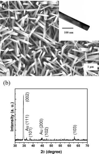
Fig. 1(a) presents the general morphologies and structures of the product. The product consists of nanowires with a hexagonal cross section, diameters of around 70 – 200 nm, and length of several mm. The inset in Fig. 1(a) displays a transmission electron microscope image of an individual ZnO nanowire, which reveals a straight and uniform nanowire along its entire length. Selected area diffraction of the nanowire (not shown here) indicates the wire is single-crystalline with c-axis oriented along its long axis.Fig. 1(b) presents a typical XRD pattern of the ZnO nanowires. The diffraction peaks were indexed and showed a hexagonal wurtzite-structure with lattice constants a ¼ 0:324 and c ¼ 0:524 nm. Au (111) and (200) peaks have been detected in several samples and no diffraction peaks of Zn or other impurities were found in the synthesized products. The inset inFig. 2(a) shows a typical low temperature PL spectrum measured at 6 K. The features of the PL spectrum can be divided into two classifications: the near band-edge emission and the deep-level emission. The deep-level emission at around 2.5 eV is associated with either excess Zn (or oxygen vacancy) or surface state emission. The near band edge spectrum of the ZnO nanowires, including several individual emission peaks, as depicted inFig. 2(a), differs from those of GaN nanowires[18,19]. It is dominated
by the bound exciton peak at 3.370 eV, due to recombina-tion of excitons bound to donors or acceptors. Since undoped ZnO is a native n-type semiconductor, the bound exciton peak is most likely related to the excitons bound to neutral donors (D0X), even though the origin of the donor level remains a pending issue[20 – 22]. At the high energy shoulder of the D0X peak, the free exciton A transition (FXA) is observed at 3.383 eV, representing little contri-bution from the quantum confinement as presented in an earlier report in which the diameters of the wires greatly exceed 20 nm [15]. A small hump at the higher energy shoulder represents the free exciton B transition or FXA ðn ¼ 2Þ: The binding energies of the neutral–donor–exciton complexes are smaller than those of excitons bound to the neutral acceptors. Thus, the A0X emission is associated with acceptor – exciton complexes[23]. On the lower energy side of the exciton peaks, the phonon replicas of the FXA at 3.32 eV and the D0X at 3.298 eV are distinguishable by their relative energy shift from the exciton peaks of the LO phonon energy of ZnO, and this will be discussed later.
Fig. 1. (a) SEM image of the ZnO nanowires (inset showing the TEM image of single nanowire). (b) XRD pattern of the ZnO nanowires grown at 9008C.
Fig. 2(b) displays the near band-edge PL spectra of ZnO nanowires at various temperatures. As the temperature increases, the D0X peak is quenched more quickly than the FXA emission and the emission peaks move toward lower energies. Observably, the FXA emission becomes the strongest one when the temperature exceeds 75 K. The exciton linewidth is broadened due to scattering of LO phonons and the excitons become thermally ionized on raising the measured temperature. Some of the bound excitons are thermally dissociated into free excitons and its LO-phonon replicas dominate the PL spectrum. Third-order and even fourth-order LO phonon replicas are observed when the temperature exceeds 200 K, which implies strong coupling of phonon and exciton in ZnO nanowires. Finally, only free exciton emission and its first-order phonon replicas were observed at room temperature.
In the Franck – Condon model, the coupling strength of the radiative transition to the LO-phonon polarization field is characterized in the use of the Huang – Rhys factor S[24]. The relative intensity of the nth phonon replica ðInÞ is related
to the zero-phonon peak ðI0Þ by the S factor as In¼ I0ðS n
e2S=n!Þ; where n is a natural number. From the measured spectra, the S factor associated with D0X is estimated to be 0.01, but the S factor associated with FXA is around 0.39. As expected, the much larger S value of FXA indicates that the coupling of FXA to the 1LO phonon is stronger than that of D0X, and this is consistent with the ZnO/ ZnMgO MQWs system [12]. On comparison of our previous report on ZnO nanorods and the epilayer [25], the S factor correlated with FXA of the nanowires is two times larger than that of the epilayer (0.186) and slightly larger than that of the nanorods (0.325). These results imply that the strength of the free exciton – LO phonon coupling, which correlates with the crystallinity, is strong in the 1D nanostructure.
The characteristic energy of the LO phonon can be determined from the energy spacing between the exciton resonant lines and their LO phonon replicas[25]. The LO phonon energy of ZnO crystal is , 72 meV at low temperature, depicted as the dotted line for reference in
Fig. 3together with the three physical quantities, FXA-1LO, (FXA-2LO)/2, and (FXA-3LO)/3, marked with solid squares, circles, and triangles, respectively, is shown as functions of temperature. Notably, the energy softening associated with the FXA-1LO phonon approximately equals 9 meV (phonon energy of 63 meV), the total amount of energy softening of FXA-2LO is only 2 meV, while for FXA-3LO it is 6 meV. The energy softening of FXA-1LO has been observed in ZnO crystals and other polar semiconductor crystals. Absorption spectra have shown a , 10% softening of 1LO phonon energy for ZnO crystals
[27]and it is theoretically explained by the exciton – polaron model[28]. Similar phonon softening have also appeared in the low temperature PL spectra of ZnO epilayer films
[11 – 14], which are marked by an open circle and an open square inFig. 3for comparison.
Fig. 2. (a) The near band edge emission of the ZnO nanowires measured at 6 K. The inset shows the wide-ranged PL spectrum. (b) Temperature dependent PL spectra of the ZnO nanowires.
Fig. 3. The 1LO phonon energy spacing and 2LO phonon spacing versus temperature. The dash line at 72 meV is plotted as reference line. The open square and circle are the values of the ZnO film in ref.[11]and[14], respectively.
Polaron formation was used to describe the dispersion relations of phonons and excitons, which will be split into two new phonon-like and exciton-like dispersion curves under the strong exciton – phonon coupling[23]. Because ZnO has a free exciton binding energy of 60 meV, which is almost resonant with the LO phonon energy of 72 meV, the excitation is transferred to the excitonic polaron. However, the bound exciton – phonon coupling of ZnO is far from resonance because of the relatively small binding energy of the bound exciton (, several meV). This explains the fact that the S-factor of FXA-1LO is much larger than that of D0X-1LO.
We also indicate inFig. 3that all the phonon energy of the phonon replica declines with the temperature increasing over 75 K. The temperature-dependence of the phonon energy shift can be explained by Permogorov’s theory[29], which states that
(i) the shift of the spectral maximum from its low-energy threshold increases linearly with temperature, D ¼ ðL þ 1=2ÞkBT; and hence also the energy spacing
between the zero-phonon and its phonon replicas; (ii) the probability of one phonon scattering is
approxi-mately proportional to the excitonic kinetic energy, i.e. ð3=2ÞkBT or L ¼ 1; and
(iii) for two phonon scattering, the annihilation prob-ability is independent of the excitonic kinetic energy, that is L ¼ 0:
The temperature dependence of the various phonon replicas of FXA of our ZnO nanowires shows basically linear behavior beyond 75 K with the slope of the temperature dependent curve of FXA-1LO replica approxi-mately equal to ð23=2ÞkB; in accordance with the
Permo-gorov’s theory, but it becomes flattened below 75 K as indicated inFig. 3. However, the slope is close to 2kBfor
FXA-2LO and close to ð21=2ÞkBfor FXA-3LO. The larger
slope for the FXA-2LO line might be attributed to combination of the second order exciton phonon scattering and cascading phonon scattering. It is still an open issue. On the other hand, the strong exciton and phonon interaction leads to the excitation of the excitonic polaron with large energy softening of the FXA-1LO phonon, which causes a flattening of the curve at low temperatures in the energy spacing versus temperature plot in Fig. 3. The phonon scattering processes become dominated at temperatures higher than 75 – 100 K, which is roughly equal to an energy spacing between 6 and 9 meV. The flattening effect also appeared in GaN films inFig. 3of Ref.[26]at around 15 K or , 1 meV, which is the energy spacing of the exciton – phonon interaction of GaN.
4. Conclusions
The LO phonon-assisted luminescence of the
donor-bound excitons and free excitons in ZnO nanowires were studied at various temperatures. The strong exciton – phonon coupling in ZnO nanowires affects not only the S factor but the FXA-1LO phonon energy spacing, which can be explained by the excitonic polaron formation. The S factor associated with FXA of the nanowires is larger than that of the epilayer. The flattening of the energy spacing of FXA-1LO phonon replicas is attributed to formation of the excitonic polaron and the exciton – phonon scattering dominates when the temperature exceeds the binding energy of the excitonic polaron.
Acknowledgements
This work has been partly supported by the National Science Council of the Republic of China under Contract No. NSC 92-2112-M009-037 and 89-E-FA06-AB. Mr Hsu is pleased to thank NSC for providing a fellowship and Chin-Ching Lin for help in the TEM measurement.
References
[1] X.F. Duan, Y. Huang, Y. Cui, J.F. Wang, C.M. Lieber, Nature 409 (2001) 66.
[2] X.F. Duan, Y. Huang, R. Agarwal, C.M. Lieber, Nature 421 (2003) 241.
[3] M.H. Huang, Y.Y. Wu, H. Feick, N. Tran, E. Weber, P.D. Yang, Adv. Mater. 13 (2001) 113.
[4] W.I. Park, D.H. Kim, S.W. Jung, G.C. Yi, Appl. Phys. Lett. 80 (2002) 4232.
[5] J.J. Wu, S.C. Liu, Adv. Mater. 14 (2002) 215.
[6] C.J. Lee, T.J. Lee, S.C. Lyu, Y. Zhang, H. Ruh, H.J. Lee, Appl. Phys. Lett. 81 (2003) 2648.
[7] C.H. Liu, J.A. Zapien, Y. Yao, X.M. Meng, C.S. Lee, S.S. Fan, Y. Lifshitz, S.T. Lee, Adv. Mater. 15 (2003) 838.
[8] M.H. Huang, S. Mao, H. Feick, H.Q. Yan, Y.Y. Wu, H. Kind, E. Weber, R. Russo, P.D. Yang, Science 292 (2001) 1897. [9] D.M. Bagnall, Y.F. Chen, Z. Zhu, T. Yao, M.Y. Shen, T. Goto,
Appl. Phys. Lett. 73 (1998) 1038.
[10] T. Makino, C.H. Chia, N.T. Tuan, Y. Segawa, M. Kawasaki, A. Ohtomo, K. Tamura, H. Koinuma, Appl. Phys. Lett. 76 (2000) 3549.
[11] Y. Chen, H.J. Ko, S.K. Hong, T. Yao, Appl. Phys. Lett. 76 (2000) 559.
[12] H.D. Sun, Y. Segawa, M. Kawasaki, A. Ohtomo, K. Tamura, H. Koinuma, J. Appl. Phys. 91 (2002) 6457.
[13] H.J. Ko, Y.F. Chen, T. Yao, K. Miyajima, A. Yamamoto, T. Goto, Appl. Phys. Lett. 77 (2000) 537.
[14] Y. Chen, S.K. Hong, H.J. Ko, M. Nakajima, T. Yao, Appl. Phys. Lett. 76 (2000) 245.
[15] W.I. Park, Y.H. Jun, S.W. Jung, G.-C. Yi, Appl. Phys. Lett. 82 (2003) 964.
[16] Q.X. Zhao, M. Willander, R.E. Morjan, Q.H. Hu, E.E.B. Campbell, Appl. Phys. Lett. 83 (2003) 165.
Roos, J.P. Spatz, H. Rauscher, S. Riethmuller, M. Moller, J. Appl. Phys. 93 (2003) 6252.
[18] C.C. Chen, C.C. Yeh, Adv. Mater. 12 (2000) 738.
[19] S.C. Lyu, O.H. Cha, E.-K. Suh, H. Ruh, H.J. Lee, C.J. Lee, Chem. Phys. Lett. 367 (2003) 136.
[20] D.C. Look, J.W. Hemsky, J.R. Sizelove, Phys. Rev. Lett. 82 (1999) 2552.
[21] C.G. Van de Walle, Phys. Rev. Lett. 85 (2000) 1012. [22] S.F.J. Cox, E.A. Davis, S.P. Cottrell, P.J.C. King, J.S. Lord,
J.M. Gil, H.V. Alberto, R.C. Vila˜o, J. Piroto Duarte, N. Ayres de Campos, A. Weidinger, R.L. Lichti, S.J.C. Irvine, Phys. Rev. Lett. 82 (1999) 2552.
[23] C.F. Klingshirn, Semiconductor Optics, Springer, Berlin, 1994.
[24] B. Di Bartolo, R. Powell, Phonon and Resonance in Solids, Wiley, New York, 1990.
[25] H.C. Hsu, Y.K. Tseng, H.M. Cheng, J.H. Kuo, W.F. Hsieh, J. Cryst. Growth 261 (2004) 520.
[26] S.J. Xu, W. Liu, M.F. Li, Appl. Phys. Lett. 77 (2000) 3376. [27] W.Y. Liang, A.D. Yoffe, Phys. Rev. Lett. 20 (1968) 59. [28] Y. Toyozawa, J. Hermanson, Phys. Rev. Lett. 21 (1968) 1637. [29] S. Permogorov, in: E.I. Rashba, M.D. Sturge (Eds.), Excitons,