INTRODUCTION
Copper has been considered as a substitute for Al-alloy metallization for future generations of on-chip interconnections, due to its high electromigration endurance and low resistivity. Electromigration (EM) of metal interconnects is a primary mecha-nism that causes interconnects to fail.1,2As devices scale down, given present-day device layouts and ground rules, the majority of resistance-capacitance (RC) delay is due to capacitive loading. Therefore, the use of low dielectric constant polymers in con-junction with a high conductivity interconnect metal offers significant performance gains.3
Polyimide (PI) is one type of long-chain macromol-ecule with a repeating monomer and a feature of cross-link between monomer chains, which provides high rigidity. Polyimide films are one of the most at-tractive interlayer dielectrics because of their good surface planarization characteristics, low residual stress, and low dielectric constant.4However, inter-diffusion was observed between the copper and poly-imide interface after annealing of the Cu film.5The diffused copper formed clusters inside the poly-imide, which raised both the dielectric constant and the dissipation factor of the polyimide and, conse-quently, degraded the properties of the polyimide.6 The impurities C and N diffused from the polyimide
into the Cu films cause resistance changes in the Cu metallization.7
The tetraethyl orthosilicate (TEOS) SiO2 films, deposited by the decomposition of TEOS, offer many attractive properties, such as low temperature depo-sition, no gas-phase nucleation, and excellent step coverage and moisture protection.8,9 The effect of TEOS SiO2 on the electromigration damage of Cu with PI passivation is studied. The TEOS SiO2films are applied between Cu and polyimide passivation to prevent the interdiffusion between PI and Cu in this research. The curing (imidization) process of polyimide is explored with thermal analyzers and infrared spectroscopy.
EXPERIMENTAL PROCEDURES
Six-inch-diameter p-type (100) Si wafers with nominal resistivity of 1 to 10 ⍀-cm were used as substrates. After standard RCA cleaning (a cleaning process for silicon semiconductor device fabrication technology developed by RCA Laboratories, USA), 50 nm thermal oxide was grown at 950°C in a steam atmosphere. The SiO2coated Si substrate was then processed with conventional photolithography to ob-tain the test pattern. Samples with positive photore-sist patterns were transferred to a vacuum chamber for the sputtering of Cu film.
The Cu film, 300-nm thick, was direct current (DC) sputtered in Ar ambient (99.999% purity). The sput-tering power was 1500 W for Cu. The base pressure of
Curing of Polyimide and the Effect of the TEOS SiO
2
Barrier
Layer on the Electromigration of Sputtered Cu with Polyimide
Passivation
HANYI HUNG and BI-SHIOU CHIOU
Department of Electronics Engineering and Institute of Electronics, National Chiao Tung Univer-sity, Hsinchu, Taiwan
The curing process of polyimide and the electromigration of copper films with polyimide (PI) passivation are studied. Thermal analysis of polyimide suggests that imidization completes at ⬃200°C with an endothermic reaction associated with the breaking of the C-OH and N-H bonds as revealed by Fourier transfor-mation infrared spectroscopy (FTIR). Although there is 89.8% weight loss when PI is heated from 20°C to 200°C, outgassing of PI passivation is still observed at higher temperatures. Carbon, nitrogen, and oxygen atoms diffuse into Cu dur-ing thermal processdur-ing of PI/Cu films. The tetraethyl orthosilicate (TEOS) SiO2 films are used as the barrier layer between PI and Cu to retard the poisoning of Cu. The effect of TEOS SiO2film on electromigration of Cu is investigated.
Keywords: Polyimide, electromigration, curing process, imidization
(Received December 20, 2000; accepted August 28, 2001) 82
Curing of Polyimide and the Effect of the TEOS SiO2Barrier Layer
on the Electromigration of Sputtered Cu with Polyimide Passivation 83
the deposition chamber was below 5 ⫻ 10⫺7torr, and the Cu film was sputtered at a pressure of 6 mTorr. After deposition of the Cu film, samples were sub-jected to a lift-off process to produce a pattern for an EM damage test.
The TEOS SiO2 films, with 50-nm or 150-nm thickness, were deposited onto some of the Cu films with plasma enhanced chemical vapor deposition (PECVD) at 250°C and 100 mtorr. Then, the poly-imide 2610 (PI2610) was statically dispensed and spun on top of TEOS SiO2. The dispense-and-spread cycle was carried out at 1500 rpm for 20 sec and the final ramp cycle was 6000 rpm for 30 sec. A two-step bake of PI was held on a hot plate, which was held at 90°C and 150°C on separate hot plates for 90 sec and 10 min, respectively.
The polyimide-coated samples were then processed with conventional photolithography to open contact vias through PI. Curing (completely imidized) of PI was done on a hot plate at 240°C, with 4°C/min heat-ing rate, for 1 h. Usheat-ing patterned PI film as a mask, BOE [mixtures of hydrofluoric acid and ammonium fluoride (NH4F0), known as buffered oxide etch (BOE)] was applied to etch the TEOS SiO2layer. For samples without TEOS SiO2, polyimide 2610 was dis-pensed and spun onto Cu films. The curing and pho-tolithography of PI were the same as described previ-ously. Blanket Al was then deposited on the specimen for the EM test by the thermal coater, which was fol-lowed by photolithography. The solution consisting of H3PO4:HNO3:CH3COOH:H2O ⫽ 50:2:10:9 was used to etch excess Al. Samples were then annealed in air ambient at 400°C for 1 h.
The electromigration tests were performed in a quartz tube at temperatures ranging from 200°C to 250°C in air atmosphere. The four input/output (I/O) pads of the samples were connected to a constant current source and a microvoltage meter.
RESULTS AND DISCUSSION
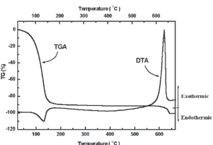
A thermogravimetric analyzer (TGA) and differen-tial thermal analyzer (DTA) are used to study the curing of polyimide. Figures 1 and 2 are the TG/DTA curves of the polyimide in N2 and air ambient, re-spectively, with a heating rate of 4°C/min. A weight loss of 89.8% was observed as PI was heated in air from 20°C to 200°C (Fig. 2), which indicates the evaporation of solvent in polyamic acid solution. The small weight loss between 200°C and 600°C , i.e., 2.5% for PI in N2and 2.3% for PI in air ambient, sug-gests that polyimide is stable below 600°C in both N2 and air ambients. The DTA curve indicates an en-dothermic reaction at 200°C. This enen-dothermic reac-tion can be related to the imidizareac-tion process, as shown schematically in Fig. 3 such that the observed energy is provided for the breaking of chemical bonds of C-OH and N-H. There is a strong exother-mic reaction of polyimide in air ambient around 640°C but not in an N2ambient. This is due to the pyrolytic reaction of polyimide yielding carbon monoxide and carbon dioxide as the major decompo-sition in air ambient.10 The slight weight loss
be-tween 200°C to 600°C in the TG curve shown in Figs. 1 and 2 suggests outgassing of PI at above 200°C.
Figure 4 is the IR spectra of polyimide cured at various temperatures. As shown in Fig. 4, absorption peaks of polyimide are as follows:C6H5U of phenyl groups (1510 cm⫺1),CuOof CuO (1712 cm⫺1),CUO of CUO (1257 cm⫺1), CUC of CUC (1118 cm⫺1), UNHUCOU of amino groups (1615, 1550, and 1319 cm⫺1), and NUCOUof imide groups (1774 and 1365 cm⫺1).11,12 The decreased absorbance of
CUO indi-cates the release of water in a polyamic acid unit structure. The increased absorbance of imide groups and decreased absorbance of amino groups suggest that amic groups condense to form imide rings.12 Comparing IR spectra of imide and amino groups, the 1 h curing at 240°C is sufficient to complete the imidization process. Also, Fig. 4 indicates that 150°C curing is not high enough for imidization to occur.
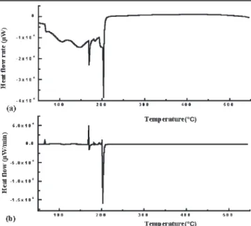
Figure 5 gives the differential scanning calorime-try (DSC) and differential of differential scanning calorimetry (DDSC) curves of PI2610 in an air ambi-ent. The DDSC data suggest that imidization of PI begins at 169°C and stops at 202°C. This is consis-tent with the IR spectra shown in Fig. 4 that PI2610 exhibits high absorbance of the imide group and low absorbance of the amino group after curing at 240°C and above.
Fig. 1. The TG and DTA curves of PI2610 in N2ambient, heating
rate: 4°C/min.
Fig. 2. The TG and DTA curves of PI2610 in air ambient, heating rate: 4°C/min.
The resistivity of as-deposited and as-annealed Cu films are 2.15 ⍀-cm and 1.8 ⍀-cm, respec-tively. The resistivity of a metal film can be ex-pressed with Mattiessen’s rules:13
(1) (2) where T is the temperature-dependent resistivity caused by the thermal phonons, and ris the resid-ual resistivity resulted from scattering of the elec-trons due to static defects such as film surface scat-tering (s), impurities (i), intragrainular defects (d), and grain boundaries (g). For a film thickness d much larger than the mean free path of the elec-trons,scan be approximated as follows:14
(3) where 0is the bulk resistivity of Cu (i.e., 1.7 ⍀-cm14), P is the probability for reflection at the surface,13,15
ρS =ρ0
( )( )
3 8 λ d( )
1−P ρr =ρs +ρi +ρd+ρgρ ρ= T+ρr
Fig. 3. Schematic diagram for the imidization of PI2610.10
Fig. 4. Infrared spectra of polyimide cured at various temperatures.
Curing of Polyimide and the Effect of the TEOS SiO2Barrier Layer
on the Electromigration of Sputtered Cu with Polyimide Passivation 85
and is 39 nm for electrons in Cu.16The film thick-ness is 300 nm. The maximum value of sis 0.083 ⍀-cm for P ⫽ 0. Hence, surface scattering is not a major contribution of Cu resistivity.
The x-ray diffraction results suggest that the an-nealed Cu films have better crystallinity than the as-deposited ones. The SEM microstructures indi-cate that the average grain size of Cu films grow from 54.5 nm for the as-deposited films to 430 nm for annealed films. Hence, the decrease of resistivity from 2.15 ⍀-cm for as-deposited film to 1.8 ⍀-cm for annealed film can be attributed to less grain boundary scattering for the annealed films.
Copper films prepared in this study have a tem-perature coefficient of resistance (TCR) of 2750 ppm K⫺1as compared to the reported data of 3000 ppm K⫺1.17The resistivity of the copper film in this study was 1.8 ⍀-cm as compared to the reported data of ⬃1.9 ⍀-cm for sputtered copper,14⬃1.67 ⍀-cm for bulk Cu,16and ⬎2 ⍀-cm for chemical vapor deposi-tion (CVD)18and metalorganic chemical vapor depo-sition (MOCVD)14Cu films. The low resistivity and low TCR of the film guarantee small electric resist-ance over a wide range of temperature and low tem-perature rise due to joule heating.
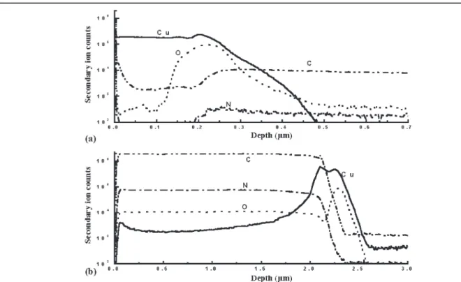
There is an 89.8% weight loss of polyimide be-tween 20°C and 200°C, presumably caused by sol-vent evaporation and outgassing, during curing (as illustrated in Figs. 1 and 2). However, outgassing is still observed during subsequent annealing. Figure 6 shows the secondary ion mass spectrometer (SIMS) depth profile of Cu and PI2610/Cu film, which were annealed at 400°C for 1 h. Low second-ary ion counts of C, N, and O atoms were observed in Cu film, as shown in Fig. 6a. Figure 6b shows high
secondary ion counts of C, N, and O atoms (1 ⫻ 104⫺ 2 ⫻ 106). During the annealing of PI/Cu film, C, N, and O diffuse into the copper film and change the resistivity of the Cu (i.e., poison effect).
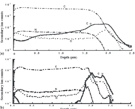
In order to retard poisoning of Cu, a TEOS SiO2 barrier layer was deposited between polyimide and Cu films. Figure 7 shows SIMS depth profiles of PI2610/TEOS SiO2/Cu films annealed at 400°C for 1 h and thermally aged at 200°C for 1 day. On the basis of the SIMS results, 150 nm TEOS SiO2is thick enough to retard the diffusion of C into Cu after 1 h at 400°C and 1 day at 200°C, while 50 nm TEOS SiO2is not.
The resistance to EM damage of Cu is also im-proved with a thicker TEOS SiO2 barrier layer. As indicated in Fig. 8, the resistance change of PI-Cu with 150 nm TEOS SiO2is much smaller than that of PI-Cu with 50 nm TEOS SiO2. A 4% resistance in-crease is observed for the sample with 50 nm TEOS SiO2after 0.04 h at 250°C and 2 ⫻ 106A/cm, while it takes 27.4 h for the specimen with 150 nm TEOS SiO2under the same stress conditions.
The kinetics of EM damage was studied using the isothermal resistance change analysis method. The resistance increases more rapidly at higher soaking temperatures. By defining a resistance change of 4% as the criterion of early stage failure, i.e., assuming the dimensions of the maximum voids are much less than the line width, the time rate change of electri cal resistance due to electromigration damage is thermally activated and can be expressed by the fol-lowing empirical equation:19
(4) dR dt R Aj Q kT 1 o n = exp
(
−)
dR dtwhere R0is the initial resistance at a given temper-ature, A is a pre-exponential factor, jn is the elec-tron current density raised to the nth power, T is temperature, and is the activation energy for EMD. The activation energy of sputtered Cu with the 150 nm TEOS SiO2 barrier layer obtained from a versus 1/T plot, shown in Fig. 9, is 0.82 eV. The activation energy for surface migration is 0.47 eV,20and the activation energy for interface mi-gration ranges from 0.7 eV to 1 eV.21Therefore, the dominant mass transport path in the PI/TEOS SiO2/Cu system is through interface.
CONCLUSIONS
The metallization system of Cu and polyimide 2610 was prepared for the electromigration test and
ln dR dt ×R 1 o
the properties of PI were studied. The DDSC analy-sis illustrated that imidization of polyimide com-pleted at 202°C, which was much lower than the conventional curing temperature. The FTIR spectra confirmed the imidization of polyimide after 1 h at 240°C. The weight loss observed at temperatures above 202°C is attributed to the outgassing of PI films. The TG/DTA curves suggest that the poly-imide is thermally stable up to 600°C.
Fig. 7. The SIMS depth profiles of PI-Cu with (a) 50 nm TEOS SiO2and (b) 150 nm TEOS SiO2barrier layer. Sample annealed at 400°C for 1 h
and aged at 200°C for 1 day.
Fig. 8. Relative resistance as a function of current stressing time at 250°C and 2.0 ⫻106A/cm2for PI-Cu with (a) 50 nm TEOS SiO
2and
(b) 150 nm TEOS SiO2barrier layer.
Fig. 9. The versus 1/T for Cu film with the PI2610/150
nm TEOS SiO2/Cu structure during the EMD test. Current density:
2.0 ⫻106A/cm2. ln dR dt 1 Ro ×
Curing of Polyimide and the Effect of the TEOS SiO2Barrier Layer
on the Electromigration of Sputtered Cu with Polyimide Passivation 87
There is 91% weight loss as PI is heated from 20°C to 400°C and outgassing of PI film is observed. Outgassing from the polyimide (primarily in the form of C) poisons the copper film and accelerates EM damage. A barrier layer of 150 nm TEOS SiO2 film between PI and Cu proves to be effective in re-tarding the poisoning of Cu.
The activation energy of Cu electromigration for PI/150 nm TEOS SiO2/Cu is 0.82 eV. The dominant mass transport path is through the TEOS SiO2/Cu interface.
ACKNOWLEDGEMENT
This work is sponsored by the National Science Council, Taiwan, under Contract No. 88-2216-E009-012.
REFERENCES
1. C.Y. Liu, C. Chen, C.N. Liao, and K.N. Tu, Appl. Phys. Lett. 75, 58 (1999).
2. C.-K. Hu, K.Y. Lee, L. Gignac, and R. Carruthers, Thin
Solid Films 308–309, 443 (1997).
3. C.-K. Hu, B. Luther, F.B. Kaufman, J. Hummel, C. Uzoh, and D.J. Pearson, Thin Solid Films 262, 84 (1995). 4. T. Homma, Mater. Sci. Eng. 23, 243 (1998).
5. H.W. Wang, B.S. Chiou, and J.S. Jiang, J. Mater. Sci.:
Mater. Electron. 10, 267 (1999).
6. H.W. Wang and B.S. Chiou, J. Mater. Sci.: Mater. Electron. 11, 17 (2000).
7. J.S. Jiang and B.S. Chiou, Int. J. Microcircuits Electron.
Package 22, 395 (1999).
8. S. Wolf, Silicon Processing for VLSI Era (Long Beach, CA: Lattice Press, 1990), vol. 2, p. 198.
9. C.Y. Chang and S.M. Sze, ULSI Technology (New York: McGraw-Hill Book Co., Inc., 1996), p. 246.
10. D.S. Soane and Z. Martynenko, Polymers in Microelectrics:
Fundamentals and Applications (Amsterdam,
Nether-lands: Elsevier Science Publishers B.V., 1989), p. 153. 11. T.C. Chang, K.H. Wu and Y.S. Chiu, Polym. Degrad. Stab.
63, 103 (1999).
12. P.D. Chung, Master’s thesis, National Chiao Tung Univer-sity, Hsinchu, Taiwan, June 1997.
13. P.L. Rossiter, The Electrical Resistivity of Metals and
Al-loys (New York: Cambridge University Press, 1987), pp. 9,
185, 218, and 290.
14. S. Riedel, J. Röber and T. Gessner, Microelectron. Eng. 33, 165 (1997).
15. M.S.P. Lucas, J. Appl. Phys. 36, 1632 (1965). 16. S.P. Murarka, Mater. Sci. Eng. 19, 87 (1997).
17. D. Save, F. Braud, J. Torres, F. Binder, C. Müller, J.O. Weid-ner, and W. Hasse, Microelectron. Eng. 33, 75 (1997). 18. J.B. Webb, D. Northcott, and I. Emesh, Thin Solid Films
270, 483 (1995).
19. B.H. Jo and R.W. Vook, Appl. Surf. Sci. 89, 237 (1995). 20. B.H. Jo and R.W. Vook, Thin Solid Films 262, 129 (1995). 21. F. Fantini, J.R. Lloyd, I.D. Munari, and A. Scorzoni,