i
金屬氧化物薄膜與奈米微結構之多功能電漿
處理與光電應用
Multifunctional Plasma Treatment on Metal Oxide Thin Films and
Nanostructures for Photovoltaic Device
研究生: 陳大方
Student: Naratip Chantarat
指導教授: 陳三元
Advisor Professor: San-Yuan Chen
國立交通大學
材料科學與工程學系博士班 博士論文
A Dissertation
Submitted to Department of Materials Science and Engineering
College of Engineering
National Chiao Tung University
in Partial Fulfillment of the Requirements
For the Degree of
Doctor of Philosophy
In
Materials Science and Engineering July 2011
Hsinchu, Taiwan, Republic of China
i
金屬氧化物薄膜與奈米微結構之多功能電漿
處理與光電應用
研究生: 陳大方 指導教授: 陳三元 教授國立交通大學
材料科學與工程學系博士班
摘要
為了滿足全世界提升太陽能轉換效率的目標,對於發展與部署大規模、省錢、可重複利用 的能源有相當的需求。近年來,在透明導電基板上,有機或是無機材料製成的太陽能電池 ,都具有良好的能量轉換效率。透明導電基板或是奈米微結構可讓光通過以被底下的活性 材料層吸收,更可將電子從此光伏器裡傳導出。這些將是此論文探討的主題。 第一部份,噴霧沉積的方式用來探討載氣中氧成份對 FTO 薄膜造成的影響。此載體 含有不同濃度的氧和氮 (0, 20, 50, 80 and 100%) ,導致對薄膜厚度、晶格長成的大小 和形狀有顯著不同。此種方式沉積而得的薄膜具有很低的電阻率約為 10-4 Ω-cm,對 550nm 光波約有 76%~96%的透光率。最後,此種光電效應製成的染料敏化太陽能電池以及高分子 太陽能電池皆顯示特別的性質,例如電荷傳導,重組以及針對表面和介面效應而成的均化 特性。 然而對於非晶質太陽能電池,作為透明基材的 FTO 薄膜,經氫化處理後會變質。因 此,此研究係針對ㄧ種雙層結構的透明導電薄膜(AZO/FTO),結果發現 AZO 的存在可保護ii 底下的 FTO 薄膜表面不受氫離子或是氫的自由基破壞,提供良好的磊晶介面。更近一步, 在經過 400 度的再退火,藉由 Sn 和氧鍵結的再氧化,可復原已被氫離子破壞的 FTO 薄膜 ,此氫離子擴散和 Sn-O 氧化還原的過程皆,經由 XPS 和 SIMS 做詳盡分析。 第二部份主要著重在選擇性的電漿處裡,針對表面的官能化,保護層的形成,以及 蝕刻,來製備奈米柱、奈米線和奈米管。因此,我們製造 P 型 SnO2的透明導電電極,是 藉由氮氣電漿將 In 和 N 共同參雜到已參雜不同濃度 In 的 SnO2薄膜。根據 In 參雜濃度, In 和 N 共同參雜的 SnO2薄膜可製備成 p 型或是 n 型,其中氮原子藉由取代 SnO2中氧的位 置,可提升其導電性、霍爾遷移率、以及 In 參雜原子的溶解度。此特性也顯著的呈現在 pn 包覆核層的異質介面,顯示 IV 曲線的對稱性以及精準二極體特型。 同樣的方法也更近一步的用來比較室溫下經由氮氣電漿處理的 ZnO 的奈米線和奈米管。經 過 900 秒處裡,ZnO 的奈米管展現高穩定性的光學反應特性,優於奈米線約 20 倍,且結 構維持完整。這代表奈米管其極高的表體比,對於表面修飾、藉由氮離子修補氧缺陷、及 ZnO 中的雜質,為指標性關鍵。 另一方面,我們提出一種選擇性的氧電漿蝕刻技術,藉由已合成的 ZnO 奈米柱為犧牲基材 ,再將 FTO 奈米粒子藉由簡單的噴霧熱解法沉積其在 ZnO 奈米柱表面,形成 ZnO-FTO 的異
質結構奈米管。XPS 分析顯示氧電漿處裡可降低 O2-/ OH -濃度比,而引起 Zn-O 鍵結的解離, 以及 Zn 離子的向外擴散,形成內部中空的結構,其可由 FTO 表面羥基官能團的形成來解 釋。藉由反覆 UV 光照射,隨時間變化的光電流測量,驗證此結構具有光感應性,且其暗 電流三倍優於未經電漿處裡的試片。
iii
Multifunctional Plasma Treatment on Metal Oxide Thin
Films and Nanostructures for Photovoltaic Devices
Student: Naratip Chantarat
Advisor: Professor San-Yuan Chen
Department of Materials Science and Engineering
National Chiao Tung University
Abstract
To satisfy the universal goal of improving solar-energy conversion efficiency, the need to develop and deploy large-scale, cost-effective, renewable energy is becoming increasingly important. In recent years, a solar cell consisting of organic or inorganic materials along with good transparent conducting oxide (TCO) films has achieved good power conversion efficiencies (PCE). Transparent conducting oxide (TCO) films or nanostructures serve as a window for light to pass through to the active material beneath and as an ohmic contact (electrode) for carrier transport out of photovoltaic. All detailed studies will become the focus in this thesis.
In the first part, a spray deposition process was used to investigate the effect of oxygen content in the carrier gas on FTO film morphology and properties. The carrier gas containing various O2/N2 concentrations (0, 20, 50, 80 and 100%) led to significant change in thickness, size
and shape of grain growth. The deposited films reach a low resistivity of ~10-4Ω-cm and a transmittance of 76%~96% at 550 nm. Finally, photovoltaic implement of dye-sensitized solar cells (DSSCs) and polymer-based solar cells reveals the particular behaviors such as charge
iv
transport, recombination, and collection properties respected to the surface and interfacial effects.
However, in case of amorphous silicon solar cells (a-Si:H), it was found that a hydrogenated effect results in the deterioration of FTO film as TCO electrode. Therefore, a double-layered transparent conducting AZO/FTO thin film was investigated and the results suggest that the AZO film acts as a protecting layer for the beneath FTO film surface, providing an excellent epitaxial interface, from the direct bombardment of H ions and radicals. Moreover, following by a post-annealing treatment at 400oC, the degraded properties of FTO can be recovered via the reoxidization of Sn-O bounds, in which H-ions diffusion and Sn-O redox process was interpreted by XPS and SIMS analysis.
In the second part, the investigation is mainly focused on a selective plasma-treatment technique for introducing surface functionalization, passivation, and etching to form nanorods (NRs), nanowires (NWs) and nanotubes (NTs). Herein, we fabricate the p-type SnO2-based
transparent conducting electrode which was constructed by a novel approach of In and N co-doping by nitrogen plasma (5-40 min), to In-doped SnO2 films with several In contents (0, 3, 7,
15 and 30%). Depending on In doping concentration, (N, In)-codoped SnO2 can be modified to
either p-type or n-type where N atoms primarily substitute in O sites in SnO2 with enhanced
conductivity, Hall mobility and solubility of the In dopant. Significantly, such behavior is also exhibited in term of pn core-shell heterojunction, showing the symmetrical I-V curve with rectified diode characteristics.
Furthermore, similar method was applied to investigate the key aspects in comparison between ZnO NWs and NTs under nitrogen plasma treatment at room temperature condition. Upon an extended treatment of 900 s, the ZnO NTs exhibit higher reliability of photoresponse,
v
20 times of NWs without deteriorated structure. This indicates that higher surface-to-volume ratio of NTs is critically important factor for inducing the surface modification, occupying the oxygen defects and impurities in the ZnO matrix by the presence of N ions.
On the other hand, we proposed a selective oxygen-plasma-etching technique for the formation of ZnO-FTO heterostructure nanotubes using presynthesized ZnO nanorods (NRs) as sacrificial templates, and FTO nanoparticles are deposited onto the ZnO nanorods by a simple spray pyrolysis method. XPS analysis demonstrated that the oxygen-plasma treatment decreased the O2-/OH- concentration ratio, resulting in dissociation of the Zn-O bonds and the outward diffusion of Zn cations to form an interior hollow, which is related to the formation of the hydroxyl functional group, Sn-OH, at the FTO surface. Time-dependent photocurrent (I-T) measurements under ON-OFF cycles of UV illumination confirms a rectified photoresponse characteristic and a dark current increased by about 3 orders of magnitude over that of the unetched sample.
vi
Acknowledgements
First and foremost I would like to express my deep and sincere gratitude to my supervisor Professor San-Yuan Chen. I appreciate all your contribution of time, ideas, and funding to my PhD experience productive and stimulating. You have taught me, both consciously and un-consiously, how a good scientist should act. Your joy and enthusiasm for research, conscientious attitude towards work, creativity and good organization was contagious for me. Importantly, you are also quite open-minded which gave me enough freedom to design my research orientation.
Another “Big Thank You” will go to Dr. Chin-Ching Lin, my co-advisor. Despite your busy schedule, you managed to have meetings with me regularly throughout my PhD. You have always been very encouraging to come up with some brilliant ideas when I was in the bottleneck of the projects. There are so many things I could learn from you as a successful scientist.
I am deeply grateful to Dr. Dean-Mo Liu, who gave me many suggestions, detail supervision and encouragement, especially during our group meeting. I have learnt so much from the way of your concepts, and there are so much effort that you put on to transform me into an independent researcher. I would honestly say that you are a person who every student can dream of. I truly appreciate that.
Beside my advisors, my research would not be completed without supporting staffs, Mei-Ching, Yu-wei, Po-Hsueh and other co-workers from NCTU and ITRI. I am free from the hustle of exhaustive experiments and technical works. Thank you for all kindness for sharing me Taiwanese’s culture and life. Although my poor Chinese becomes a huge barrier to communicate
vii
fluently, I felt that everyone was so patient to talk and listen to me; I cannot thank you enough for that.
Dear all Thai friends, you all are like my brother and sister. We could always enjoy life (exercises, drinks, foods, etc.) together, because we know this is what life is about! Thank you for a lot of accompanies and I wish you all the best for life, studies and future careers. Although time passed too quickly, TSAX (Thai student association in Xin-Chu) must go on to facilitate all the members, especially new comers and confederates.
Dear mom, dad and elder brother, no words can express my gratitude to you for giving me life, educating me, and your conditional love. All I have achieved today would not be possible without the love from all of you. As an old Chinese saying “with elderly parents at home, filial son must not travel far”, I really appreciate your understanding and support when I studied abroad to pursue my interests.
Last but not least, this thesis is dedicated to my other-half, Shu Han. You have walked into my life six years ago, fulfilling my life with joy, satisfaction and happiness. We have been through every good and bad moment hand-in-hand. We have grown up strongly while seeking a better future together. Thank you for staying beside me (always) as best friend, critic and my lover.
Naratip Chantarat
Hsinchu, Taiwan
viii
Contents
Chinese abstract ... i
English abstract ... iii
Acknowledgement ... vi
Contents ... viii
Figure captions ... xi
Table and scheme captions ...xvi
Chapter 1 Introduction...1
Chapter 2 Literature Review and Theoretical Framework ...5
2.1 Wide band-gap metal-oxide materials ...5
2.1.1 Background of metal oxide nanostrucutres: ZnO and SnO2 ...5
2.2 The State-of-Art of Defect Chemistry in Metal Oxide Materials ...7
2.2.1 Electronic and optical properties ...7
2.2.2 Band-gap Engineering ... 11
2.3 Surface modification in nanoscience and nanotechnology ... 15
2.3.1 Surface passivation ... 15
2.3.2 Surface treatment by plasma ... 18
2.3.3 Surface etching by plasma ... 24
2.4 Solar cells-based Transparent Conducting Oxide (TCO) semiconductors ... 28
2.4.1 Perspectives and evolutions of solar cells ... 28
2.4.2 Hydrogenated amorphous silicon (a-Si-H) solar cells ... 28
2.4.3 Dye-sensitized solar cells (DSSCs) ... 30
Chapter 3 Experiment methods ... 37
3.1 Experiment overviews ... 37
3.2 Preparation of metal-oxide materials ... 38
ix
3.2.2 Fabrication of Al-doped ZnO (AZO) film on FTO ... 39
3.2.3 Synthesis of ZnO nanorods (NRs), nanowire (NWs) and nanotubes (NTs) ... 39
3.2.4 Preparation of O2 plasma-etched ZnO/FTO heterostructure nanotubes ... 40
3.2.5 Preparation of n-type ZnO/p-type (N, In):SnO2 core/shell heterojunction diode .. 40
3.3 Characteristics analysis ... 41
Chapter 4 Effect of Oxygen Patial Pressure on the Microstructural Growth and Physical Properties of Transparent Conducting Fluorine-Doped Tin Oxide Thin Films Fabricated by Spray Pyrolysis Method ... 43
4.1 Introduction ... 43
4.2 Formation and microstructure of FTO texture films ... 44
4.3 Optical and electrical properties ... 49
4.4 Performance of photovoltaic devices... 52
4.5 Summary ... 57
Chapter 5 Mechanism of a AZO-coated FTO Film in Improving the Hydrogen Plasma Durability of Transparent Conducting Oxide Thin Film for Amorphous-Silicon Based Tandem Solar Cells ... 58
5.1 Introduction ... 58
5.2 Surface morphology and structural properties of single-layered FTO films and double-layered AZO/FTO films ... 60
5.3 Evolution of transparent conducting films under H-plasma treatment ... 63
5.4 Diffusion mechanism of hydrogen-incorporated atoms ... 69
5.5 Summary ... 75
Chapter 6 Nitrogen Plasma-Assisted Co-doped P-type (In, N):SnO2 Ultra-Fine Thin Films and N-ZnO/p-SnO2 Core-Shell Heterojunction Diodes Fabricated by an Ultrasonic Spray Pyrolysis Method ... 77
6.1 Introduction ... 77
6.2 Fabrication and physical properties of In-doped SnO2 films ... 80
x
6.4 N-ZnO/p-SnO2 Core-Shell Heterojunction Diodes ... 90
6.5 Summary ... 94
Chapter 7 Enhanced UV Photoresponse in Nitrogen Plasma ZnO Nanotubes ... 95
7.1 Introduction ... 95
7.2 Chemical growth of ZnO nanorods (NRs) and nanowires (NWs) ... 96
7.3 Effect of N-plasma treatment on ZnO nanostructures ... 97
7.4 Photoresponse characteritics ... 100
7.5 Summary ... 102
Chapter 8 Selective Oxygen-Plasma-Etching Technique for the Formation of ZnO-FTO Heterostructure Nanotubes and Their Rectified Photocatalytic Properties ... 104
8.1 Introduction ... 104
8.2 Microstructure of FTO-coated ZnO nanorod arrays... 107
8.3 Oxygen-plasma-etching mechanism on ZnO nanorod templates ... 107
8.4 Photoresponse of ZnO-FTO composite nanotubes... 117
8.5 Summary ... 119
Chapter 9 Conclusion ... 120
9.1 Investigation of TCO thin film electrode for photovoltaic devices ... 120
9.2 Plasma treated metal oxide thin films and nanostructures ... 121
References... 123
Cirriculum Vitae ... 134
xi
Figure captions
Figure 2.1 Structures of (a) wurtzite ZnO and (b) cassiterite SnO2 [26, 27]. ...6
Figure 2.2 Schematic diagrams of charge transport in the energy transitions from the valence band to the conduction band [35]... 10 Figure 2.3 Illustration of band alignment and the Schottky barrier formed at the junction of conducting oxide (ITO) and semiconductor (TiO2) (a) before and (b) after H2-gas reduction [49].
... 12
Figure 2.4 (a) Structure and (b) equilibrium energy band diagram of the CuYO2:Ca/ZnO/ITO
p-i-n heterojunction diode coated on glass substrate [52]. ... 14 Figure 2.5 IDS-VDS curves (at different gate biases: 6, 8 and 10 V) and IDS-VG curves (at
VDS=0.1 V) of a ZnO nanowire FET under ambient air, dry O2, and vacuum conditions as
compared between (a, c) before and (b, d) after PMMA passivation, respectively [56]. ... 16 Figure 2.6 SEM images of SnO2-ZnO core-shell where the SnO2 nanofiber was synthesized
by electrospinning and the ZnO outer layer was deposited with different ALD cycles of (a) 0, (b) 100, and (c) 400 [10]. ... 17 Figure 2.7 (a) TEM image of a ZnO-SnO2 core-shell nanorod where the inset shows a
magnified image of the crystal fringes in the SnO2 shell. (b) High-magnification TEM image
reveals misfit dislocation in the SnO2 epitaxial layer. (c) Schematic model of the atomic
arrangements of the SnO2 hexagonal nanoring on the (100) plane surrounding a ZnO nanorod on
the (0001) plane [62]. ... 18 Figure 2.8 Schematic drawing of ZnO nanowire shows (a) the influence of physisorbed water molecules in air, capturing free electron and inducing a low-conductivity depletion layer at the nanowire surface. The current is increased under a vacuum condition due to a desorption of the water molecules. (b) Upon illumination with UV in air, electron-hole pairs are generated, while the carriers are decreased with the replacement of the hydroxyl group by oxygen ions from the steady light [57]. ... 20 Figure 2.9 XPS spectra of O 1s core level from untreated and oxygen plasma treated (5-30 min) ZnO films [74]. ... 20 Figure 2.10 (a) Idealized energy band diagram for an Au/SnO2 interface. Band alignment of Au
xii
Structures of the SnO2 films exposed under different oxygen plasma-treated time (30 and 180 s)
[76] ... 22 Figure 2.11 Illustration of the colloidal lithographic concept with some 2D geometrical
structural units: (a) hexagonal double layer, (b) hexagonal triple layer (HCP), (c) hexagonal triple layer (FCC), (d) square double layer, and (e) square triple layer [91]. ... 25 Figure 2.12 SEM images of the resultant embossed TiO2 films coated on polystyrene bead
templates (a) without O2 plasma etching, and O2 plasma etching for (b) 2 min and (c) 4 min. (d)
Cross-sectional TEM image of a hollow TiO2 hemisphere with TiO2 film deposition at intervals
as shown in the inset. (e) High-magnification TEM image from the TiO2 shell showing
polycrystalline layer with thickness (~150 nm) and grain sizes (10-30 nm) [60]. ... 26 Figure 2.13 Flowchart for ordered silica nanotube arrays, fabricated by using vertical silicon nanowire templates [59]. ... 27 Figure 2.14 Schematic representation of the principle of the dye-sensitized photovoltaic cell operating under illumination [97]. ... 31 Figure 2.15 Schematic drawing of the DSSC. An array of Zn microtips, grown vertically from conductive glass electrode and decorated with ZnO nanotip hierarchy, serves as the photoanode [101]. ... 34 Figure 2.16 Interfacial electron transfer via dye, TiO2 particle, and TCO electrode, involving a
trapping/detrapping process [104]. ... 35 Figure 2.17 Directing the flow of photogenerated electrons across the nanostructured
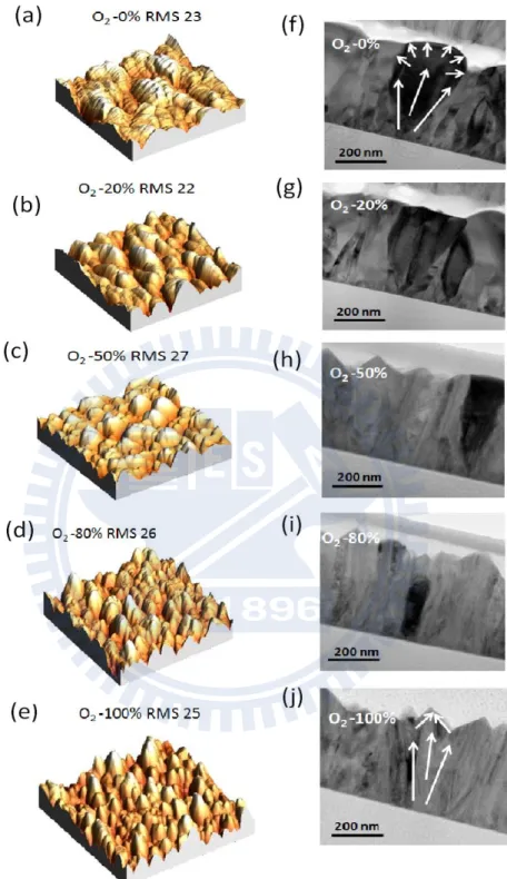
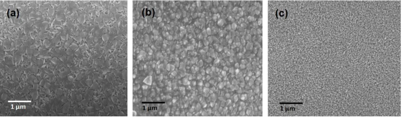
semiconductor ZnO NW/ZnO NP composite and the possible electron transport mechanism regarding to the annealing treatment process [105]. ... 36 Figure 4.1 (a-e) AFM topographic 5×5µm scans and (f-j) cross-sectional TEM images for oxygen-incorporated FTO films deposited at various oxygen concentrations: 0, 20, 50, 80 and 100%... 46 Figure 4.2 FE-SEM images of the deposited FTO films on glass substrate as a function of oxygen content: (a) 0%, (b) 20% and (c) 100%. ... 47 Figure 4.3 X-ray diffraction (XRD) patterns of FTO films deposited on glass substrate with O-incorporated various concentrations.. ... 49 Figure 4.4 Transmission (T%) spectra of FTO films of varying oxygen concentration,
xiii
Figure 4.5 FTO film electronic-transport properties: carrier concentration (n), resistivity (ρ), and Hall mobility (µ) as a function of the oxygen concentration (0-100%).. ... 51 Figure 4.6 J-V characteristics of FTO film-based DSSCs. The illumination intensity of 100 mW cm-2 with AM 1.5 and active area of 0.25 cm2 were applied.. ... 53 Figure 4.7 Representative Nyquist plot of the electrical impedance spectra of the FTO films measured in the frequency range of 0.1Hz – 1MHz under AM 1.5.. ... 54 Figure 4.8 Trace of current density against voltage (J-V) for three cells with 0%, 20% and 100% O2/N2 concentrations.. ... 56
Figure 5.1 Plain-view SEM images of the textured FTO films and the AZO/FTO films (a and d) without H2 plasma treatment, or with H2 plasma treatment for (b and e) 5 min , and (c and f)
30 min.. ... 61 Figure 5.2 X-ray diffraction pattern of the FTO, AZO, and AZO/FTO samples before and after H2 plasma treatment for 30 min as identified at each spectrum.. ... 62
Figure 5.3 (a) Cross-sectional TEM image of a double AZO/FTO film coated by a thin Pt conductive layer. (b) High-magnification TEM image taken from the region, marked by a square in (a).. ... 63 Figure 5.4 Dependence of (a) carrier concentration, (b) Hall mobility, and (c) sheet resistance on H2 plasma treated time for the deposited FTO, AZO, and AZO/FTO films.. ... 64
Figure 5.5 The effect of (a and b) H2 plasma treatment at 0, 5, 10, 20 and 30 min, and (c and
d) post annealing treatment at 400oC on the optical transmission for the FTO and AZO/FTO films.. ... 67 Figure 5.6 SIMS depth profiles of (a and b) FTO and (c and d) AZO/FTO films for secondary ion count of Sn, F, O, and H normalized relative to FTO. The plasma-treated samples and the post-annealed samples are represented by S2 and S3, respectively.. ... 70 Figure 5.7 X-ray photoelectron spectra of the F 1s peak observed for (a) FTO and (b)
AZO/FTO samples with as-deposited condition (S1), 30-min plasma treatment (S2), and post annealing process, subsequently. The deconvoluted peaks F1 and F2 indicate a major component (Sn-F bond) and a minor component (C-F bond), respectively.. ... 72
xiv
Figure 5.8 The variation of [Sn]/[O] atomic intensity ratios for the FTO and AZO/FTO films corresponding to the surface of as-depostied films (S1), the surface of H-plasma exposed films (S2), and the surface of subsequently annealed films (S3). The insets show the relative Sn (3d3/2)
and Sn (3d5/2) core level spectra.. ... 74
Figure 6.1 XRD peaks of In-doped SnO2 films prepared by ultrasonic spray pyrolysis method
with In concentrations: 0, 3, 7, 15 and 30 at%.. ... 81 Figure 6.2 UV-vis absorption spectra of the In-doped SnO2 film deposited on corning glass
substrate with various doping concentrations. The optical transmission demonstrates the spectral continuity in range of 300-700 nm.. ... 82 Figure 6.3 The In doping concentrations (0, 3, 7, 15 and 30 at%) during the film fabrication are shown in (a), (b), (c), (d) and (e), respectively, and the annealing temperature is constant at 600oC. Comparing dark current of as-deposited and annealed SnO2 films undergoing the post
plasma treatment (0-40 min).. ... 84 Figure 6.4 (a) XPS spectra of the N 1s peak observed for (N,In) co-doped SnO2 samples
treated in N plasma for 0, 10 and 40 min. (b) AES depth profiles of the sample in (a) at 40 min, and the etching rate of Ar+ for 1 sec is equal to 3 Å in penetration depth.. ... 89 Figure 6.5 (a) Top view and (b) cross section SEM images of In:SnO2-coated ZnO nanorod
arrays. The inset shows a high magnification of top view image. (c) TEM images illustrate a pn heterojunction core-shell consisted of p-layer In:SnO2 and n-layer ZnO with their lattice images
and FFT patterns as identified by yellow.. ... 91 Figure 6.6 (a) I-V characteristics of the pn heterojunction diode in dark using an applied voltage in range of +/-1eV . The inset gives the I-V characteristics of individual p-type In:SnO2
and n-type ZnO films. (b) The energy band diagram at equilibrium.. ... 93 Figure 7.1 FESEM images: of (a) ZnO NWs and (b) NTs; HRTEM images (c) NWs and (d) NTs on glass substrates subjected to post annealing at 300oC and nitrogen plasma treatment.. ... 97 Figure 7.2 Photoluminescence spectra measured at room temperature for a nitrogen plasma treatment of 0, 60 and 720 s for (a) ZnO NWs and (b) NTs.. ... 98 Figure 7.3 (a) Current as a function of applied voltage for both ZnO NWs and NTs, with and without a 900 s nitrogen treatment. (b) Dark current dependence versus N2-exposure time.. ... 99
xv
Figure 7.4 (a) Time traces of the current with the chopped light for samples measured after a 900 s N2 plasma exposure under an applied voltage of +1 eV (electron conduction). The inset
shows the schematic diagram of the corresponding measurement method. (b) Energy-band
diagram for 300 ◦C annealed and N2 plasma-treated ZnO under UV illumination.. ... 101
Figure 8.1 Field-emission SEM images of (a) as-deposited ZnO NRs grown on a Corning glass substrate using a hydrothermal method and (b) FTO coating on ZnO NRs obtained by spray pyrolysis deposition. The FTO deposition time was 2 min at 380oC.. ... 107 Figure 8.2 HRTEM images of core-shell ZnO-FTO heterostructures (a) before and (b) after exposure to oxygen plasma for 20 min at room temperature. The insets of parts a and b show the magnified interface, indicated by the red rectangle.. ... 108 Figure 8.3 Cross-sectional HRTEM and EDS line scans of an ZnO-FTO nanotube fabricated by dry oxygen-plasma etching at 20 min: (a and b) side view; (c and d) top view.. ... 109 Figure 8.4 Formation of voids in the FTO-coated ZnO obtained before and after etching of ZnO NRs as a function of time: (a) 0min; (b) 2min; (c) 20min. The inset of part b is a high-resolution image of the void.. ... 110 Figure 8.5 XRD patterns of as-grown ZnO and ZnO-FTO heterostructures on glass treated for the times noted under oxygen plasma. The patterns are vertically offset for clarity.. ... 111 Figure 8.6 PL of (a) as-grown ZnO and (b) FTO-coated ZnO samples showing variation of the spectrum intensity corresponding with the plasma exposure time. The insets of parts a and b demonstrate the morphology of the ZnO NRs after 20 min of etching and the relative intensity (R) of part b, respectively.. ... 112 Figure 8.7 XPS spectra of the O 1s peak in FTO-coating ZnO samples: (a and b) before and (c and d) after plasma etching (350-W RF power for 20 min), preparing the samples with and without preheat annealing at 500oC, as indicated in each figure.. ... 114 Figure 8.8 Under UV illumination (λ=365nm), with an applied voltage of +5 eV (electron conduction), τg1and τg2 are shown indicating the response times of time-dependent photocurrent
xvi
Table and scheme captions
Table 2.1 Formation energy (eV) of N-doped SnO2 atom supercells in O-rich condition and
Sn-rich condition [38].. ...9 Table 4.1 Summary of FTO film properties used in DSSCs. ... 53 Table 4.2 Summary of photoelectric conversion efficiencies for a selection of polymer solar cells.. ... 57 Table 6.1 The results of Hall effect measurements of the annealed In:SnO2 samples
corresponding to 0-30% In doping concentration with a selective N-plasma treatment at 40 min.. ... 87 Scheme 4.1 Schematic cross section of polymer solar cells deposited on an FTO-coated glass substrate, using an oblique electron-beam evaporation method.. ... 55 Scheme 5.1 Illustration showing the cross-sectional structure of FTO and AZO/FTO films and the possible H-ion diffusion mechanism under different conditions. ... 75 Scheme 6.1 Illustration of the corresponding current-voltage (I-V) measurement set-up. The deposition and post plasma process applied to fabricate the p-In:SnO2/n-ZnO core-shell
heterojunction using ZnO nanorods as a template. ... 92 Scheme 8.1 Top-View Cross-Sectional Schematic Diagram of an FTO-Coated ZnO Core-Shell Nanostructure, Illustrating the Oxygen-Plasma Enhanced Etching Evolution of the ZnO-FTO Nanotube a (a The direction of outward diffusion is indicated by the arrow in stage 3). ... 117
1
Chapter 1
Introduction
During the past decade, it is increasingly clear that the global reliance on exhaustible natural resources (e.g. oil, ethanol, natural gas and coal) must shift in favor of using sustainable strategies and renewable energy sources in order to provide more environmentally production route. One renewable resource that has the capability to meet the increasing energy demand comes in the form of solar radiation. The direct conversion of solar energy to electricity attributed to photovoltaic effect has a significant impact allowing clean, unlimited-source, reliable, and cost-efficient methods. However, one of major components in photovoltaic cells relies on semiconductor materials that involve the use of sophisticated technologies with high production cost. Thus, significant cost reductions using novel strategies must be considerably necessary to compete with other traditionally generated power.
Transparent conducting oxides (TCOs) that provide thermal stability, high transparency, and oxidation resistance have yet to be widely used in electronic, optoelectronic and photovoltaic applications [1-4]. The components of TCOs are mainly composed of the wide band gap metal oxides with unintentional n-type conductivity generated by intrinsic defects and the inadvertent incorporation of other impurities. For example, the role of oxygen vacancies (Vo) is predominant
for the electronic properties. Consequently, the large oxidizing power of charge transport in metal oxide coupled with low-cost production renders it the semiconductor materials of choice for many applications that exploit solar energy conversion efficiency.
2
Among the metal oxide materials, there are a large number of options for improving solar cell performance by the use of nanomaterials as building blocks for devices. This can help downscale conventional technologies by developing a miniaturization of functional units with its unique physical and chemical properties. In particular, low-dimensional, nanostructured materials have attracted much attention because of their large surface-volume characteristics, which promote some advantages such as superior sensitivity to light, electrical transport, and lower charge carrier recombination. Moreover, the effect of defects on the physical properties can significantly increase with decreasing in dimension of material. In this thesis, of particular interest is also the use of plasma technology to deliver high throughput, conformal coverage, and reproducibility of gaseous treatment at low substrate temperature, for high surface reactive nanostructures. Especially, a high aspect ratio of 1D nanostructures such as nanorod [5, 6], nanowire [7, 8], core-shell nanowire [9, 10], nanotube [11, 12], etc. could be more effective with plasma than other alternative nanostructures or textured films when quantum confinement, charge-carrier collection and transport are determined by low trapping/detrapping.
For the purpose to develop new technique for the metal oxide surface modification, particularly using in solar cell applications, Chapter 4 firstly demonstrated the fundamental investigation of the effect of oxygen content on FTO film morphology and properties. The various ratios of O2/N2 carrier gas led to significant change in thickness, size and shape of grain
growth of FTO films, which is indicative of variable conditions to study the role of correlation between optical and electrical properties. As the result, high film quality was obtained at a low resistivity of ~10-4Ω-cm and a transmittance of 65%~92% (λ=550 nm). Moreover, photovoltaic implement of dye-sensitized solar cells (DSSCs) also revealed the particular behaviors such as conversion efficiency, charge transport, recombination, and collection properties. With this
3
investigation, the model will examine the concept in understanding the mechanism of ion-incorporated film and the defect state behavior, which is fundamentally important to the rest of following studies.
In Chapter 5, we proposed the development of double-layer TCO electrode that involves an additional AZO barrier layer coating on the FTO layer. The deterioration of FTO film properties might be reduced when the products were exposed to hydrogen plasma atmosphere during the fabrication process of hydrogenated amorphous silicon (a-Si:H) solar cells. This configuration was confirmed by the structural (SEM, TEM, XRD, XPS and SIMS), optical (UV-Vis), and electrical (Hall measurement) characterizations that the AZO layer is able to protect the FTO film from the bombardment of H-ions and radicals. Finally, a systematic study of the post annealing treatment reveals a recovery of the deteriorated properties of FTO films through the diffusion mechanism of incorporated hydrogen in the films.
Chapter 6 demonstrates a novel methodology for developing co-doped p-type SnO2 films
using dual acceptors (In and N elements). The deposited films were delivered by ultrasonic spray pyrolysis containing mixed solution of In and Sn precursors in combination with thermal annealing at 600˚C and post nitrogen-plasma treatment. In this chapter, not only the film characteristics with different conditions will be presented, but also this technique can be adapted to use in 1D-nanoscale, e.g., core-shell nanowire. Because the ultrafine p-SnO2 thin film with
controllable size (~10 nm in thickness) and texture suites with such selective plasma treatment method (reactive ion etching; RIE), this nano-heterojunction seems to behave the same way as a conventional thin film diode. Therefore, we produced n-ZnO/p-SnO2 core-shell diode using ZnO
4
nanorods as a template, which represents another technological challenge for a variety of applications in nanoscience.
Similar to Chapter 6, the investigation in Chapter 7 is involved with the influence of nitrogen plasma on chemically grown ZnO nanowire (NWs) and nanotubes (NTs). This section discusses, for the first time, the photoluminescence (PL), dark current (I-V measurement), and photoresponse (I-T measurement) behavior due to a change of the surface defect; indicating that the oxygen defects and impurities are occupied by the presence of N ions in the ZnO matrix.
Finally, Chapter 8 demonstrates the use of a selective oxygen-plasma etching technique to fabricate ZnO-FTO composite nanotubes. In this approach, presynthesized ZnO nanorod arrays act as templates, and FTO nanoparticles are deposited onto the ZnO nanorods by a simple spray pyrolysis method. Upon high power of oxygen plasma treatment, various ions and radicals (O+, O2+, and O*) generated by the oxygen plasma, readily diffuse into oxygen vacancies and create negative charges on the ZnO NR surface. Then, with prolonging the treatment time, the accelerated etching rate might occur to produce a large number of voids in the ZnO surface and form a hollow ZnO-FTO heterostructure, respectively. In addition, an etching mechanism via oxygen plasma will be tentatively discussed along with examining a rectified photoresponse and dark current characteristics compared with the as-synthesized sample.
5
Chapter 2
Literature Review and Theoretical Framework
2.1 Wide band-gap metal-oxide materials
During the past decades, metal oxide semiconductors have attracted much research attentions in a wide range of advanced applications such as electronics, optoelectronics, sensors, photocatalysts, field emissions, solar cells, etc. [13-17]. It is known as one of the material compounds containing transition elements and oxygen. So, for example, the oxide materials can provide various utilizations from additional doping incorporation due to its variable bandgaps across the infrared to ultraviolet regions. Moreover, the excellent chemical and thermal stabilities have commonly been observed based on the recognition that metal-oxide bound exhibits durable from dissolution in acidic and basic solutions and very high decomposited temperatures (more than 1000˚C), respectively.
2.1.1 Background of metal oxide nanostrucutres: ZnO and SnO
2Among the metal oxide proposed as wide band gap materials, Zinc oxide (ZnO) is one of the most extensively studied, owing to unique multiple properties such as high electron mobility, piezoelectric, pyroelectric, and strong room-temperature luminescence. Crystalline ZnO has a wurtzite type of crystal structure under ambient conditions. The wurtzite structure has a hexagonal unit cell with two lattice parameters (a and c), in which either Zn or O atom displaces with respect to each other along the threefold c-axis. Figure 2.1a shows tetrahedrally coordinated Zn2+ and O2- ions with alternating planes stacked layer by layer along the c-axis direction. The
6
bonds between cation (Zn) and anion (O) possess a strong ionic interaction that the opposite charges result in a spontaneous polarization and piezoelectricity with normal dipole moment. For an electrostatic point of view, this polarity is an important factor in crystal growth, defect generation, plasticity, etching, etc. In addition to polar surfaces, it also introduces the four most common faces of wurzite ZnO including the polar Zn-terminated (0001), O-terminated (0001�) faces (c-axis) and the nonpolar (21�1�0) and (011�0) faces [18]. Therefore, various shapes of the ZnO crystal are originated due to the configurations; differences in the growth rates of different crystal planes, which can also be facilitated for the fabrication of novel nanostructures. Due to its diverse and rich structures and properties with low-cost strategies, recently, many types of nanostructured ZnO including nanowires [19], nanoneedles [20, 21], and tubular whiskers [22] have already been synthesized mainly by hydrothermal growth, atmospheric spray pyrolysis, and vapor-liquid-solid (VLS) depositions [23-25].
7
Tin oxide (SnO2) is another important n-type semiconductor regarded as an
oxygen-deficient material. Its large bandgap (Eg = 3.6 eV at 300 K) makes it ideally working as a
transparent conducting electrode for a wide range of industrial applications [28-31]. Structurally, SnO2 can be formed by two natural oxidation states, Sn(II) and Sn(IV). The dominant crystal
structure of the products is commonly described as cassiterite or rutile-structured SnO2, which is
composed of the tetragonal unit. In a tetragonal unit cell, three-fold coordinated oxygen atoms surround the octahedral coordinated tin atoms as shown in Figure 2.1b. To activate the surface stability of such cassiterite structure, some energy (temperature in the range of 350-600oC) is required to keep balance between the number of the dangling cation bonds and the dangling anion bonds. Furthermore, the unique properties were arisen when nanosized dimensions occur in crystal structure through fabrication processes. The synthesis and growth of a certain morphology can be selectively controlled by the assembly of the building blocks [32-34]. Therefore, by exploiting the special electrical and optical properties of nanomaterials, there is a great potential as well as fundamental prerequisite for the development of nanoscience and nanotechnology, which will be a major discussion in the following sections.
2.2 The State-of-Art of Defect Chemistry in Metal Oxide Materials
2.2.1 Electronic and optical properties
The structural imperfections in crystals can be commonly defined as “point defects”, when either atoms in the host crystal (intrinsic) or additive chemical impurities (extrinsic) is not in regular lattice position. The presence of point defects or impurities plays a major role in determining the electrical and optical properties of the host crystal.
8
The most dominative intrinsic point defect is a lattice vacancy, which is a missing atom or crystalline site. Given the importance of some binary oxide based semiconductors (e.g. CdO, In2O3, SnO2, ZnO) [35], it has been postulated that a native point defect, such as oxygen
vacancies, clearly establishes its prevailing n-type character according to: 𝑂�� ↔ 1/2𝑂�(𝑔) + 𝑉�∙∙+ 2𝑒′. In principle, a generation of an oxygen defect releases two electrons, which is mainly
contributed to the shallow electron states. Another vacancy defect is an extra atom in a non-crystalline site, which is transferred from a lattice site to the interstitial position. Interstitial atoms are considered to require a large amount of energy to immigrate into a close-pack crystal. If the energy of such defect-related states happens to be much deviated from that of states of the perfect crystal, the mechanism of electrical conductivity will be significantly affected by the motion of diffused atoms or ions. However, it becomes an important consequence that all types of metal oxide materials may not occur in the same configuration because their corresponding interstitial formation reactions yield noticeably different oxygen partial pressure (𝑝𝑂�) dependence of conductivity [36].
The addition of a foreign atom in the fraction of a host crystal atom is known as “extrinsic point defect”. When the proper proportion of doping impurities was applied, the substitutions will take the place of a normal atom at the lattice site at equilibrium state, hence improving the operation of physical properties. Based on atomic size and formation energy considerations, substitutional impurities introduces relevant charge states differently within the band gap: (1) “deep level” is referred to the energy of the impurity-related states near the middle of band gap, while (2) it provides “shallow level” when the states lie close to the valence band (VB) or conduction band (CB). One example of such SnO2 doping of Group-V elements (N, P,
9
mechanism in metal oxide semiconductor. Generally, it has been established that undoped SnO2
crystal typically exhibit n-type conductivity due to the presence of its native point defects; tin interstitials (Sni) and oxygen vacancies (Vo). The electronic-structure calculations revealed that
P, As and Sb strongly prefer to occupy the Sn sites to enhance “n-type conductivity” of as-grown SnO2, in which the extra electrons in states below the CB freely move in the host matrix. In
contrast, N is preferentially incorporated to the anion O sites (No), which has the lowest
formation energy among other possible N defects under both O- and Sn-rich conditions (Table 2.1) [38], and act as a deep acceptor (p-type conductor). This is because the empty states known as “hole” was left right on the top of VB after N atom-occupied O site stimulates an electron to be excited out of the filled valence band to higher level states. Upon incorporation of donor or acceptor doping atoms, similar electronic-transition effects have also been reported in other metal oxide semiconductors such as binary oxides: Ga2O3 [39], Fe2O3 [40], TiO2 [41], MgO
[42], ternary oxides: CuAlO2 [43], SrCu2O2 [44] and even co-doped metal oxides: (H,
Al)-codoped ZnO [45], (N, F)-Al)-codoped TiO2 [46], etc.
Table 2.1 Formation energy (eV) of N-doped SnO2 atom supercells in O-rich condition and Sn-rich
10
Not only doping techniques have been broadly used to enhance the conductivity and the stability of various metal oxide thin films by modifying the energy band structure, but also optical transitions between impurity levels or other occupied conduction states could be a critical role to achieve optical property enhancement through absorption or emission characteristic of photons. Taking n-type TCOs (Sn-doped In2O3; ITO) as a prototype [36, 47], a high optical
transparency is mainly determined by the factor: the fundamental band gap (Eg) becomes larger
in fact up to ~1eV, with increasing carrier concentration from electron doping impurities. Figure 2.2 shows the magnitude of the shift (∆BM), indicated as dark area, due to the Burstein-Moss
effect, which is attributed to allowed transition between the fundamental conduction band edge and the second conduction band (SCB). However, the band-gap shrinkage or renormalization (∆RN) occurs inversely due to an increase in the energy of the valence-band maximum (VBM)
and decrease in the energy of the conduction-band minimum (CBM), when the excess of charge carriers was applied in the conduction band. Finally, the optical transparency in the visible wavelength range is maintained, defined as a difference of the two contributions, ∆Eg = ∆BM -
∆RN. Somehow, the findings could be also adapted for understanding charge transport in
optoelectronic devices based on other wide-band gap metal-oxides.
Figure 2.2 Schematic diagrams of charge transport in the energy transitions from the valence band to the
11
2.2.2 Band-gap Engineering
In doping semiconductors, band-gap engineering in term of analytical model demonstrates how the presence of charge carrier concentrations based on external dopants is so crucial for the operation of electronic devices. The model basically interprets several effects such as excitation/recombination of charge behavior within the space-charge region, interface states at a thin oxide (depleting layer), the creation of the Schottky barrier (band bending) at the interface, and tunneling effect due to highly doped concentration. The operating mechanism begins when (1) the external electric field excited electrons from the donor-related state, instead of the VBM, to the CBM. (2) Or, similarly, electrons can be also excited from the VBM to the acceptor-related state and leave a delocalized hole at the original state, if the impurity state locates much closer to the VB than the CB. Consequently, any occurrence of these two cases results in generation of electron and hole (current), flowing in the direction of the applied electric field depending on their signs (+/-).
For two parts in the contact between metal-semiconductor or semiconductor-semiconductor, so-called “spatial inhomogeneities” were normally introduced by effective Schottky barrier (ɸB) at the interface, which also correlate with noise properties of Schottky
diodes and grain boundaries [48]. The combination of the metal (or conductive oxide) electrode and the semiconductor affects the energy of electronic state on the semiconductor side. The different work functions (ϕ) between these two layers create a charge depletion region and band bending on the semiconductor, which hinder the electron transfer across the interface. However, corresponding to the relative position of Fermi levels (EF), electrons (negatively charge carriers)
move from the semiconductor (lower work function) to the metal (or conductive oxide) electrode (higher work function) until the Fermi levels align at the thermal equilibrium state. Like an
12
example as shown in Figure 2.3, when ITO transparent electrode and TiO2 are brought into the
contact [49], band alignment in a ITO-TiO2 junction induces electrons moving from one side
(TiO2) to the other (ITO), responsible for overcoming the potential (Schottky) barrier (Vs). It
indicates that the built-in barrier; 𝑞𝑉� = 𝑞(𝜙�− 𝜙�) and the shift in work function; 𝑞Δ𝜙 = 𝑞(𝜙�− 𝜒), where 𝜒, 𝜙� 𝑎𝑛𝑑 𝜙� are the electron affinity, the work functions of ITO and TiO2,
respectively. To achieve higher efficiency and yield, this work investigated a simple way to conserve the electrical conductivity of ITO films under post annealing process by applying a reducing H2 gas. As a result, this method could prevent annihilation of oxygen vacancies (free
carriers generating the electrical conductivity) from oxygen in the atmosphere. In principle, the increased optical band gap of ITO may occur because the additional donor electrons occupy the energy states above the CB, which could higher the Fermi energy level, i.e., reducing the Schottky barrier at the interface. Therefore, the H2-annealed ITO electrode was assumed to
employ significantly improved interfacial charge transport due to decreased internal resistance of the cell.
Figure 2.3 Illustration of band alignment and the Schottky barrier formed at the junction of conducting
13
Furthermore, improvement of interfacial adhesion has been a matter of intensive study. The advantages and disadvantages of various common techniques depend on a variety of factors, such as contact area, charge-transport dimensionality, structural similarity, and charge recombination. For instance, poor interfacial contact (TiO2/FTO), encountered in nanoparticulate
film-based devices, can be tailored by a UV laser welding [50]. One obvious evidence as electrochemical impedance analysis (Z) proved that the contact resistance decreased proportional to an increase in the power of laser beam upto 0.5 W. It was claimed to be a simple, fast, and adaptable for any other efficiency improvement schemes. However, since a thin region of the interface was locally involved in this technique, the experiment must be very tricky to handle. The exceeded irradiation might readily damage the TiO2 particles or even degrade the
conductivity of the ITO film.
Similarly, in the case of p-n junction, two parts in contact are basically composed of one semiconductor doped with donor impurities (n-type) and the other one doped with acceptor impurities (p-type). Due to high mobility of the carriers (electron and hole), they diffuse toward the opposite directions; electrons move to p-doped side and holes move to n-doped side. At the p-n junction, the energy bands of the semiconductors must bend, also forming a depletion region corresponding to the alignment of Fermi energy level in both p and n-doped layers. This consequence leads to a rectifying behavior in oxide materials, which has been reported in term of “homojunction” or “heterojunction” diode. Toru et al. [51] have fabricated a ZnO-homojunction diode by using laser phosphorus (P) doping to form a p-type ZnO layer on a typically n-type ZnO substrate. Band-edge emission (λ = 370-380 nm) and broad peak (λ = 400-500 nm) of the ZnO diode was revealed via the electroluminescene spectrum under forward current injection at
14
110 K. The light emission of white-violet color was observed, which is evidently caused by a band-edge component of defect states.
In addition, p-i-n (p-type/intrinsic/n-type) heterojunction diodes [52] commonly offer another approach for improving the rectifying configurations of abrupt junction in ordinary p-n diode [53]. Figure 2.4a displays the structure of transparent p-CuYO2:Ca/i-ZnO/n-ITO diode. It
concluded that using the selective materials with their proper band-gap mismatch could lead to a smooth transition as shown in Figure 2.4b. This can develop the injection of electrons from n-ITO to p-CuYO2, while the flow of space-charge-limited current is attributed to the single-carrier
injection in the i-ZnO layer. The possible applications of p-i-n diode have been widely used in many branches such as fast switches, photodetectors, and high voltage power electronics [54,
55].
Figure 2.4 (a) Structure and (b) equilibrium energy band diagram of the CuYO2:Ca/ZnO/ITO p-i-n
heterojunction diode coated on glass substrate [52].
15
2.3 Surface modification in nanoscience and nanotechnology
2.3.1 Surface passivation
A wealth of the techniques with controllable temperature and doping concentration has been widely reported by various research groups, with notable purposes including surface passivation [56], functionalization [57, 58] and etching [59, 60]. Song et al. [56] demonstrated the passivation effects of a polymethyl methacrylate (PMMA) on the electrical characteristics of ZnO nanowires, under various oxygen environments. They found that the surface passivation can prevent oxygen ions (𝑂�, 𝑂��, 𝑜𝑟 𝑂��) from being absorbed onto the defect site (𝑉���) of ZnO nanowires, where such intrinsic defects (𝑉��� and 𝑍𝑛���) attribute to the n-type conductivity in ZnO. Then, the electrical characteristics of the single ZnO nanowire with and without coating PMMA passivation surface were compared via the field effect transistors (FETs) devices under ambient air (20% O2) , dry O2, and vacuum (~10-3 Torr) environment. In Figure 2.5, the output
IDS-VDS and IDS-VG curves indicates that carrier concentration, mobility, and threshold voltage of
the as-grown ZnO nanowires were significantly influenced proportional to increasing in the contents of oxygen environment, while the passivated samples remained unchanged due to no electrons trapping to the oxygen molecules at the surface.
16
Figure 2.5 IDS-VDS curves (at different gate biases: 6, 8 and 10 V) and IDS-VG curves (at VDS=0.1 V) of a
ZnO nanowire FET under ambient air, dry O2, and vacuum conditions as compared between (a, c) before and (b, d) after PMMA passivation, respectively [56].
As mentioned above, it also suggests that the performance characteristics of heterostructure nanodevice primarily rely on the quality of growth interface. Combining two materials with the same crystal structure is assumed to offer well-defined and clean interface of the epitaxial growth films associated with passivation of surface defect density. However, this concept was also adapted for using in the epitaxial growth of other couple materials with different crystal systems. Such SnO2/ZnO heterojunction nanocatalyst core-shell was
successfully synthesized by which it exhibits the possibility of using in various types of application [10, 61, 62]. Architecturally, the 3D epitaxial heterostructure for superlattice
17
structures [63, 64], coaxial [65-68], and biaxial [69-71] nanowires or nanocables were developed and applied to the DSSCs, in order to enhance the overall device efficiencies with a consideration of high aspect (surface-to-volume) ratio and catalytic activity. Herein, to understand detailed information about the microstructure and morphology of core-shell nanowires, SEM images and their insets can be seen in Figure 2.6 that the uniform-size distribution can be readily obtained, while the shell thickness was varied with the number of the atomic layer deposition (ALD) cycles [10].
Figure 2.6 SEM images of SnO2-ZnO core-shell where the SnO2 nanofiber was synthesized by
electrospinning and the ZnO outer layer was deposited with different ALD cycles of (a) 0, (b) 100, and (c) 400[10].
However, Kuang et al. demonstrated that HRTEM images (Figure 2.7) evidently revealed more understandings about layer-to-layer interaction. As a result, although the ZnO nanorod was completely coated with a well-crystalline SnO2 layer, the lattice mismatch (misfit dislocation)
between the SnO2 shell and ZnO core might be induced due to the injection of structure defects
18
develop this strategy by selecting correlated hybrid materials in responsible with using suitable fabrication methods.
Figure 2.7 (a) TEM image of a ZnO-SnO2 core-shell nanorod where the inset shows a magnified image of
the crystal fringes in the SnO2 shell. (b) High-magnification TEM image reveals misfit dislocation in the
SnO2 epitaxial layer. (c) Schematic model of the atomic arrangements of the SnO2 hexagonal nanoring on
the (100) plane surrounding a ZnO nanorod on the (0001) plane [62].
2.3.2 Surface treatment by plasma
Several semiconducting metal oxides such as ZnO, SiO2, In2O3, and SnO2 serving as
direct wide band gap materials are strongly affected by the chemical adsorption of ambient gases. In this approach, the surface modification methods using a dry plasma treatment represents straightforward route to change the structural, optical and electrical properties via surface energy band bending due to the generation or degeneration of additional or removal molecules in defect sites.
19
In atmosphere, water molecules normally physisorb with the hydrogen sides to the metal oxide surface in order to introduce the lower free energy and the overall stability of the system. For example, the hydroxyl groups (OH-)of water molecules were weakly bound to ZnO surface at the positively charged active sites (Zn2+-OH-), which will subsequently capture the electrons as illustrated in Figure 2.8 [57, 58, 72]. According to the reason, this topic deserves further investigation regarding to the incorporation of surface treatment on the physical properties of metal oxide materials. Recently, the study of oxygen plasma assisted epitaxial ZnO thin film growth [73] revealed the creation of the rectifying behavior, therefore improving the UV detector characteristics as compared with the ohmic behavior in the untreated samples. The XPS (O 1s core level) spectra in Figure 2.9 exhibit the removal of conductive OH layer accumulated at the surface; the deconvoluted peaks show an increase in the relative intensity of the O-Zn peak to the O-OH peak when the plasma treatment time was increased. This indicates the abundance of atomic oxygen radicals filling into the oxygen vacancies of the host lattice, which is able to lower the Fermi level (EF) in the band gap and create band bending upward. The oxygen plasma
treatment not only eliminates all detectable hydroxide and hydrocarbon contaminations leading to an increase in surface conductivity, but also the formation of Schottky barrier are much suitable to gold , platinum contact, etc., due to its low oxygen affinity [74].
20
Figure 2.8 Schematic drawing of ZnO nanowire shows (a) the influence of physisorbed water molecules
in air, capturing free electron and inducing a low-conductivity depletion layer at the nanowire surface. The current is increased under a vacuum condition due to a desorption of the water molecules. (b) Upon illumination with UV in air, electron-hole pairs are generated, while the carriers are decreased with the replacement of the hydroxyl group by oxygen ions from the steady light [57].
Figure 2.9 XPS spectra of O 1s core level from untreated and oxygen plasma treated (5-30 min) ZnO
21
In case of SnO2, the surface electronic states are also affected by oxygen plasma [75, 76];
the absorbed oxygen species from oxygen plasma were expected to induce the reduced SnOx
surface, where the Sn2+-O bonds existed, by forming the damaged (depleting) layer on the surface. In a detail, this phenomenon was demonstrated by the energy level diagram in Figure 2.10. The energy bands at the surface bent upward (denoted by “ϕB”) after oxygen plasma
treatment, resulting in a surface accumulation layer and additional electron trap states. When a depleting layer was produced, the electron affinity (χ) is reduced, hence making contribution to the formation of a Schottky contact with Au electrode, used in various applications. On the other hand, to treat the samples under N2 gas annealing, the incorporation of nitrogen atoms in the
SnO2 host matrix [38, 77] introduced possible mechanisms in the opposite way. The interstitial
and substitutional N atoms preferentially located in anion sites due to low defect formation energies in the O-rich conditions. In principle, density function theory calculations revealed a major possibility that the N atoms are energetically favorable to occupy the O site within a limitation of diffusion depth. In this process, the introduction of such defects or impurities can change the surface chemistry by surface oxidation, thereby recovering the Sn4+-O bonds (SnO2
phase). This can enhance the field emission characteristics of SnO2 due to decreasing in the
22
Figure 2.10 (a) Idealized energy band diagram for an Au/SnO2 interface. Band alignment of Au contact
on (b) an as-deposited SnO2 film and (c) an oxygen-plasma treated SnO2 film.(d) Structures of the SnO2
films exposed under different oxygen plasma-treated time (30 and 180 s) [75].
As scaling down of complementary metal-oxide-semiconductor, the effect of defects on the physical properties increases with decreasing in dimension of material. The improvement of quantum physics limitation might require the ability of such plasma technology to deliver high throughput, conformal coverage, and reproducibility at low substrate temperature. For these advantages, different plasma-involved methods have recently been extended to use in the numerous applications of metal oxide nanostructure including transparent conductors [78], electrochromics [54], Li-ion batteries [79], photovoltaic cells [80], gas sensors [81], and complex oxides [43]. Typically, plasma system is used as a passivation technique by different gaseous carriers, which can effectively reduce the surface or interface trap states. Recently, a reversible process to control the characteristics of SnO2 nanowire transistors (NWTs) has been
23
(UVO) treatment, alternatively [82]. The lower concentration of Vo, which acts as a donor type
defect to produce electrons in NW, might decrease the conductivity when nitrogen ions were filled into the Vo sites. Under a subsequential treatment of UVO radiation, the O atom could
react with N ion-substituted Vo to form NOx, which is likely to detach from the surface. Finally,
the reproduced Vo was obtained leading to an increase in conductivity at its initial state.
However, this study has been found in contradictory with the other previous reports [37, 38, 83], which are related to the mechanism of N-incorporated SnO2; Pan et al. [83] examined that
atomic N could actually prefer to substitutes at O sites in SnO2, due to the lowest formation
energy among the other defects. Hall probe measurement shows the enhancement of p-type conductivity with increasing N doping concentration, in which the generation of dominative acceptors is highly possible to compensate n-type conductivity of the intrinsic defects.
Recently, semiconductor nanocrystals (quantum dots-QDs) have been used to combine with low-dimensional metal oxides to enhance the efficiency of solar cell devices because the tunable size of QDs can basically provide the ability to match their absorption wavelength with the solar spectrum. Instead of using capping or linking agent [84-87], plasma treatment becomes another suitable technique for developing interfacial properties in such hybrid materials. For example, oxygen plasma could modify ZnO NWs surface in order to improve CdSe QDs absorption [88]; O ion bombardment was assumed not only to remove the surface-bound contaminants in ZnO surface such as hydroxyl (OH) and hydrocarbon (C-H) groups, but also to create the dangling bonds of carboxyl (COOH) group on the species to increase the colloidal QDs attaching on the ZnO NW surface. A consistent result was also obtained with I-V characteristics of dye-sensitized solar device where the higher QD coverage may cause an enhancement of light absorption, electron injection, and generated photocurrent, respectively.
24
2.3.3 Surface etching by plasma
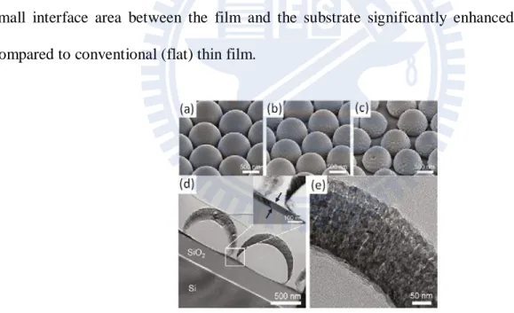
In terms of nano-architectural device, conventional lithography techniques widely offer one possibility for the fabrication of requisite structures, spanning the size in the range of 10-100 nm. There is a number of different techniques such as soft lithography [89], colloidal lithography
[90], and electron lithography [33], which were used for 2D or 3D patterned surface combined
with template-directed synthesis. Among several nanomaterials including hallow-core, tubular, porous, and nano-array structures [59, 60] have promoted unique chemical and physical properties because of their ultralarge surface areas and inherent catalytic activities. One important methodology in the lithographic process is associated with “plasma etching technology”, which allows high throughput and simple control of the operating parameters (plasma source, etching gas, flow rate, etc.). Thus, a higher scalability of selective-plasma etching has been successfully applied to remove metal oxide [59] or organic templates [60] with remaining original crystalline structures of unetched portions, as compared with thermal decomposition (the Kirkendall effect) [91] or wet chemical etching [92].
For metal oxide nanostructure, a primary technique that determines dry etching mechanism in this interest is reactive ion etching (RIE) method. It is one of most well-known methodologies in terms of top-down etching techniques, large operating area, and high density at relatively low pressure (10-1-10-4 Torr). RIE consists of a glow-discharge-generated plasma where chemically reactive gases are added to gain higher etching rates via selective bombardment of reactive species: radicals (chemical selectivity) and ions (physical removal of substrate species). In a detail, RIE introduces a negative charge (electron produced in the plasma) at the substrate, while the positive ions are simultaneously accelerated toward the surface plane resulting in a creation of more reactive surface. In this case, an anisotropic etching might be
25
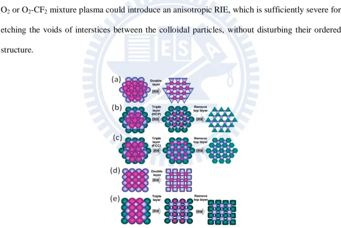
achieved and able to produce high aspect ratio features, if low plasma potentials (<100 V) and high rf biases (>500V) are applied. An example of the fabrication of binary and ternary particle arrays with nonspherical building blocks was done by RIE under O2 plasma [90]. This approach
used different structures of colloidal arrays as nanolithography masks, being self-organized, onto the PS bead-coated substrates. As illustrated in Figure 2.11, 2D patterned structures possess for organizing some common geometries, which depend mainly on two basic concepts regarding to: (1) different colloidal arrangements will give different final structures, i.e. fcc and hcp crystal structures in the stacking of the hexagonally close-packed (111) layers. (2) The use of either pure O2 or O2-CF2 mixture plasma could introduce an anisotropic RIE, which is sufficiently severe for
etching the voids of interstices between the colloidal particles, without disturbing their ordered structure.
Figure 2.11 Illustration of the colloidal lithographic concept with some 2D geometrical structural units:
(a) hexagonal double layer, (b) hexagonal triple layer (HCP), (c) hexagonal triple layer (FCC), (d) square double layer, and (e) square triple layer [90] .
![Figure 2.1 Structures of (a) wurtzite ZnO and (b) cassiterite SnO 2 [26, 27].](https://thumb-ap.123doks.com/thumbv2/9libinfo/8745804.204985/23.918.137.846.518.941/figure-structures-wurtzite-zno-b-cassiterite-sno.webp)
![Figure 2.3 Illustration of band alignment and the Schottky barrier formed at the junction of conducting oxide (ITO) and semiconductor (TiO 2 ) (a) before and (b) after H 2 -gas reduction [49]](https://thumb-ap.123doks.com/thumbv2/9libinfo/8745804.204985/29.918.109.809.382.939/figure-illustration-alignment-schottky-junction-conducting-semiconductor-reduction.webp)
![Figure 2.9 XPS spectra of O 1s core level from untreated and oxygen plasma treated (5-30 min) ZnO films [73]](https://thumb-ap.123doks.com/thumbv2/9libinfo/8745804.204985/37.918.244.641.489.888/figure-spectra-level-untreated-oxygen-plasma-treated-films.webp)
![Figure 2.13 Flowchart for ordered silica nanotube arrays, fabricated by using vertical silicon nanowire templates [59]](https://thumb-ap.123doks.com/thumbv2/9libinfo/8745804.204985/44.918.192.720.726.948/figure-flowchart-ordered-nanotube-fabricated-vertical-nanowire-templates.webp)
![Figure 2.14 Schematic representation of the principle of the dye-sensitized photovoltaic cell operating under illumination [96]](https://thumb-ap.123doks.com/thumbv2/9libinfo/8745804.204985/48.918.220.713.104.390/figure-schematic-representation-principle-sensitized-photovoltaic-operating-illumination.webp)
![Figure 2.16 Interfacial electron transfer via dye, TiO 2 particle, and TCO electrode, involving a trapping/detrapping process [103]](https://thumb-ap.123doks.com/thumbv2/9libinfo/8745804.204985/52.918.276.637.297.615/interfacial-electron-transfer-particle-electrode-involving-trapping-detrapping.webp)