14-5
2004 IEEE Asia-Pacific Conference on Advanced System Integrated Circuits(AP-ASIC2004)/ Aug. 4-5,2004
A 1.2y
18mW, lOGbls SiCe Transimpedance Amplifier
Chihun
Lee, Chia-Hsin Wu, and Shen-Iuan Liu
Graduate Institute of Electronics Engineering & Department of Electrical Engineering National Taiwan University, Taipei, Taiwan 10617, R. 0. C.
Abstract
To the authors' knowledge, the first 1.2V, ISmW, 10Gb/s SiGe transimpedance amplifier (TIA) is presented here. It has been realized in a 0 . 3 5 ~ SiGe process and its area is 0.45mmz with pads. Employing inductive series and shunt peaking techniques, the proposed TIA can achieve a transimpedance gain of 61.6dBQ and the bandwidth of 7.4GHz, while dissipating only 18mW with 1.2V supply. With an equivalent photodiode capacitance of 0.15pF, this TIA shows the input referred noise current density of 22pAi dHz.
1. Introduction
The growing popularity of multimedia applications demands high data rate wired telecommunication systems. Many existing wired systems require 10Gb/s analog kont-ends, such as OC192 for telecommunications and 10Gb/s Ethernet for data communications. The key requirements for designing a high-speed front-end are: 1)
to integrate both the high-speed analog front-end and digital back-end and 2) low voltage and low power. Traditionally, analog RF front-end utilized high fT
transistors of GaAs. However, GaAs RF circuits could not be integrated with succeeding CMOS digital processors. With the past decade, there is a significant effort to implement the multi-gigabits optical front-ends [1]-[5] in BiCMOS and CMOS technologies. It can provide the advantages of high integration and low cost.
Conventional bandwidth-enhancement techniques, such as the regulated cascode topology [2] [3] and the negative feedback configuration [I], will suffer the limitation of the supply voltage. When the deep submicron technology advances further, the low supply voltage is indispensable. In this paper, a low-voltage and low power transimpedance amplifier (TIA) utilizes the inductive series and shunt peaking techniques to improve the overall bandwidth. To save the power dissipations, this proposed TIA can provide a high transimpedance gain without a power-hungry buffer because it
uses
thesame
gain stage to match a 50-ohm resistive load directly. A 1.2 V, IgmW,1 OGbls SiGe transimpedance amplifier is implemented in a 0.35pm SiGe 3p3m process. Compared to the current high-speed TlAs [I]-[6], the proposed one can achieve the lowest supply voltage and lowest power consumption.
11. Circuit design A. Low-voltage amplifier
To develop low-voltage analog and digital circuits is
0-7803-8637-x104/$20.00~2004
IEEE.
300fi,
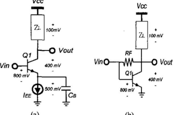
ZL IDDrnV U l m m " 1 1 - 1 1 , . f (a) (b)Fig. 1 Common emitter amplifier (a) conventional topology
(b) proposed low-voltage one.
of great interest. In [7], it is described that bipolar circuits have the iooate DC headroom problem. For the bipolar transistors with a constant current density, the base-emitter voltage (VBE) does not decrease with the scale-down technology and it has a turn-on voltage of 8OOmV. Besides, a minimum collector-emitter voltage (VcE) around 400mV can protect high-speed bipolar transistors against heavy saturation. Under a supply voltage of 1.2V, the classical cascode amplifier using bipolar devices is forbidden. Fig. I illustrates two common emitter amplifiers. The evaluation of their minimum supply voltage for a low supply voltage of 1.2V and high-speed operation are considered. In the conventional topology of Fig. l(a), it
uses a bypass capacitor CB and a tail current source.I,, that may occupy 500mV headroom in experience. Obviously, the sum of VBE in Q1 and the voltage across the tail current source will exceed the supply voltage. Fig. I(b) represents a shunt-shunt feedback amplifier with RF, which can have a dc self bias and provide input matching. When the voltage swings across Z, maintain as small as IOOmV, it is sufficient to make the amplifier operated in the supply voltage below 1V operation.
Furthermore, the voltage gain for two common emitter amplifiers in Figs. l(a) and (h) can be calculated. For the conventional commoo emitter amplifier io Fig. l(a) with the bypass capacitor, CB, the small-signal voltage gain can be
where g, is the transconductance. Since g, = IcNT, eq. (I) can he sequentially simplified as follows:
2004 E E E Asia-Pacific Conference on Advanced System Integrated Circuits(AP-ASIC2004)/ Aug. 4-5,2004
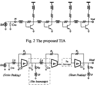
Fig. 2 The proposed TIA
Fig. 3 The small-signal model for the proposed TlA
where VT = kT/q. In eq. (2), the sufticient voltage across
ZL can increase the gain and it is especially important for
low-voltage amplifiers. Supposed that the impedance of ZL
is much smaller than RF, the low-voltage topology in Fig. I(b) can reach a similar voltage gain as Fig. l(a). By means of Miller's theorem, the input impedance of the amplifier in Fig. l(h) can be
R F - R F
1 - A
I+g,Z,
Ri,
=-- (3)Furthermore, this input impedance can be designed to match the input 5Oohm termination according to eq. (3).
B. The proposed TIA
Based on Fig. l(b), the proposed TIA is presented in Fig. 2 by using the inductive series and shunting peaking
techniques [8]. Compared to the conventional TIAs [1-5],
the proposed one can have several advantages: self-bias operation, low input impedance, and high gain for low-voltage and low-power applications.
The small-signal model for the proposed TIA is shown in Fig. 3. An inductor Ls can be inserted between a
photodiode CpD and a shunt-shunt feedback amplifier in order to increase the bandwidth. In practical, the core amplifier exhibits one pole system. Thus, series peaking with a damping factor of 1/42 can multiply the bandwidth by 1.4 times. The inductive shuntmg peaking technique is used in high-speed output buffers to ease the trade-off between output matching, speed, and voltage headroom. An inductor Lp in series with the resistance Rp can enlarge the
t- Conventional
series peaking --T--- Proposed I . Shunt peaking
1
:
"
:'
:'
I . I, .. ,, . ! :Normalized frequency
Fig. 4 Simulated bandwidths for the conventional TIA, the series peaking one, the shunting peaking one and the proposed one, respectively.
bandwidth. Therefore, the shunt peaking technique can 'also have a flat response to enhance the bandwidth by
a
factor of 1.7. The simulated bandwidth enhancement factors for the conventional TIA, the series peaking one, the shunting peaking one and the proposed one, respectively, are shown in Fig. 4. Compared to the conventional amplifier, the bandwidth enhancement factor for the conventional TIA, the series peaking one, the shunting peaking one and the proposed one is 1.4, 1.7 and 2.1, respectively. Obviously, the proposed TIA can have a larger bandwidth enhancement factor.
C. Devices selection for the proposed TIA
In considerations of DC biasing, the selection for the bipolar transistors should trade off among headroom of
VCE, collector current density (Jc), unity-gain 6equency
(fi),
gain, noise, and power consumptions. In addition, a bipolar device with Jc of 640 uA/um* is selected for the high-speed date rates of 10Gb/s. Each identical bipolar transistor in the proposed TIA obtains l . l v headroom and achieves the current gain of 160 with f,of 40GHz.111. Experimental results
The proposed TIA has been implemented in a 0 . 3 5 ~ 1 1 3P3M SiGe process and measured by on-wafer probing. Fig. 5 shows two TIAs: the top one is the proposed TIA with eight inductors and the bottom one is a series peaking TIA with four inductors. Due to high-speed considerations, the small inductors below 1nH are used. Two core circuits separately occupy the area of 900um x 400um and 900um x 200um, respectively.
Operating from the supply voltage of 1.2V, both of them consume the same current of 15mA.
2004 IEEE Asia-Pacific Conference on Advanced System Integrated Circuits(AP-ASIC2004)/ Aug. 4-5,2004
the series peaking one (bottom).
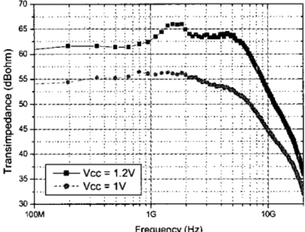
With an equivalent photodiode capacitance of 0.15pF, both TIAs are measured by on-wafer probing. For a supply voltage of 1.2V, the measured transimpedance gain for the proposed TIA and the series peaking one is 61.6dBR and 58dBR, respectively, as shown in Fig. 6(a).
The measured bandwidth, f.3dB, for the proposed TIA and the series peaking one is 7.4GHz and 4.4GHz, respectively. The measured bandwidth enhancement factor is 2.45 and 1.46 for the proposed TIA and the series peaking one, respectively. Fig. 6(b) illustrates the approximately linear phase response for both TIAs. Fig. 7 shows the transimpedance response for different power supplies. It is demonstrated that the proposed TIA can normally work 1.2V and further below 1V. Fig. 8 shows the measured 6equency response for the proposed TIA under 1.2V,
where s l l and s22 are almost below -1OdB. When the
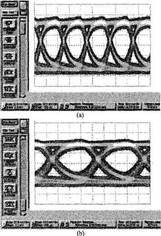
supply voltage is 1.2V, the measured eye diagrams by
PRBS of 2^''-I are shown in Fig. 9. It can achieve the highest data rate of 12.5Ghk.
70 I I I . . . . . . . . c 30 : . : . ''< 20 lOOM 1G l f f i Frequency (Hz) r i : I : I .
,
: I -1wI
0 5G 10G 1% 20G Frequency ( H r ) (h)Fig. 6 (a) the measured transimpedance gain for the proposed TIA and the series peaking one.
(b) the measured phase response for the proposed TIA and the series peaking one.
lOOM 1G
Frequency (Hr)
Fig. 7 Measured gain of the proposed TIA is 54.3 dBR and
6 1.6 d B 0 for IV and 1.2V supply voltages, respectively.
Feequency ( H r )
Fig. 8 Measured frequency response for the proposed TIA with the supply voltage 1.2V
2004 IEEE Asia-Pacific Conference on Advanced System Integrated Circuits(AP-ASIC2004)/ Aug. 4-5,2004
IV. Conclusions
Table I summarizes the measured performances of the proposed TIA, compared with other literatures. This TIA can operate under the supply voltage of 1.2V and 18mW power dissipations. To authors’ knowledge, it is the first lOGb/s SiGe transimpedance amplifier (TIA) with
I .2V supply voltage. By using both the inductive series
and shunting peaking techniques, the gain of 61.6dBR and the bandwidth of 7.4GHz can he achieved for IOGB/s applications.
Acknowledgement
The authors would like to thank National Chip lmplementation Center for chip implementation. Special thanks to Mr. Wen, Mr. Chiu, and Dr. Huang of National Nano Device Laboratory team for measurement supporting. This work was supported in part by MediaTek Inc.
V. References
[I]. B. Razavi, “A 622 Mb/s 4.5 pAIdHz CMOS transimpedance amplifier,” ISSCC Tech. Dig. pp. 162
-163,453, Feb. 2000.
W. Z. Chen and C. H. Lu, “A 2.5 Gbps CMOS optical receiver analog front-end," CICC, 2002. Proceedings of the IEEE 2002, pp. 359 -362, May 2002.
J. Lee, S-J. Song, S. M.
Park
C-M. Nam, Y-S. Kwon, and H-J. Yoo, “A multichip on oxide of I Gbis 80 dB fully-differential CMOS transimpedance amplifier for optical interconnect applications,” ISSCC Tech. Dig. pp.80 447, Feb. 2002.
H. H. Kim, S. Chandrasekhar, C. A. Burrus, and J.
Bauman, “A Si BiCMOS transimpedance amplifier for I 0-Gbis SONET receiver,” IEEE I. Solid-State Circuits,
vol. 36, pp. 169 -776, May 2001.
B. Analui and H. Ali, “Multi-pole bandwidth enhancement technique for transimpedance amplifier,” ESSCIRC 2002, Session C16, pp. 303-306, Sept. 2002
A. K. Petersen, et al.,“Front-end CMOS chipset for 10 Gbis communication,”RFIC 2002, pp. 93-96, June 2002.
B. Razavi, Y. Ota, and R. G Swartz, “Design techniques for low-voltage high-speed digital bipolar circuits,” IEEE I. Solid-state Circuits, vol. 29, pp. 332 -339, March 1994. [2]. [3]. [4]. [SI. [6]. [7].
CO)
Fig. 9 Measured eye-diagrams for the proposed TIA with input equivalent current of
lOOUAp,,
1.2V supply, and input data(a) IOGb/s of PRBS 2^”’-l (Horizontal scale: 5Ops/div, vertical scale: 2OmV/div).
(b) 12.5Gh/s of PRBS 2A3’-l (Horizontal scale: 2Ops/div,
vertical scale: 20mVidiv).
[SI. S. S. Mohan, M. M. Hershenson, S. P. Boyd, and T. H. Lee, “Bandwidth extension in CMOS with optimized on-chip inductors,” IEEE J. Solid-State Circuits, vol. 35, pp. 346 -335, March 2000
Table I. Performance summary (X: not mentioned)