國 立 交 通 大 學
電 信 工 程 學 系 碩 士 班
碩 士 論 文
積體光學電路中緩衝結構之研究
Study of Transition Structures in Integrated Optics
研 究 生 : 羅正倫
指導教授 : 彭松村 博士
黃瑞彬 博士
積體光學電路中緩衝結構之研究
Study of Transition Structures in Integrated Optics
研 究 生:
羅正倫
Student:
Cheng-Lun Lo
指導教授:
彭松村 博士
Advisor: Dr. Song-Tsuen Peng
黃瑞彬 博士
Dr. Ruey-Bing Hwang
國立交通大學
電信工程學系碩士班
碩士論文
A Thesis
Submitted to Institute of Communication Engineering
College of Electrical Engineering and Computer Science
National Chiao Tung University
In Partial Fulfillment of the Requirements
for the Degree of
Master of Science
In
Communication Engineering
July 2004
HsinChu , Taiwan , Republic of China.
積體光學電路中緩衝結構之研究
研 究 生: 羅正倫
指導教授: 彭松村 博士
黃瑞彬 博士
國立交通大學電信工程學系碩士班
摘 要
由於現在光學積體電路的尺寸不斷地在縮小,為了使能量能有效地傳輸,電 路內部用於緩衝的介質波導其設計就顯得更加地重要。我們整篇的文章將用可分 析幾乎任何形狀的階梯進似法以及波模匹配法來獲取我們所要的結果。在此,為 了簡化我們複雜的問題,我們將整個結構塞進一個全尺寸的上下平行金屬板內來 分析,並且把上下金屬板拉的夠開的狀況下去計算以逼近實際的物理狀況。在第 三章中,我們列舉了一些典型的結構,其所得到的數據以及圖表可以做為日後要 設計該緩衝介質波導時一個可依循的標準。依照我們想要的傳輸量,藉由所得的 圖表,所對應結構的尺寸大小我們可以有準則地去獲得了。Study of Transition Structures in Integrated Optics
Student:
Cheng-Lun Lo Advisor:
Dr. Song -Tsuen Peng
Dr.
Ruey
-Bing
Hwang
Institute of Communication Engineering
National Chiao Tung University
July 2004
Abstract
Due to the limitation on the size of an optical integrated circuit, the circuit topology should be simplified﹒However, to have an efficient transmission for the signal, a good design with transition structures becomes important gradually﹒In light of its unique and complex theoretical basis required, in this thesis, we present an systematical analysis for a class of transition structures by the rigorous mode matching method ﹒ In order to simply our sophisticated problem, we insert the overall structure into an oversized metallic parallel-plate waveguide﹒Furthermore, we separate the distance of the parallel-plate waveguide far enough to approximate the practical case﹒Finally, in the chapter 3, we illustrate several typical transition structures, and the numerical data we obtained later can be developed as a guideline while designing them﹒From these figures, we can easily get the size of the structure with the desired transmission efficiency﹒
誌 謝
首先,我真的很謝謝我的兩位指導老師 – 彭松村教授以及 黃瑞彬教授, 由於他們不厭其煩地教導我,使得這一篇論文能夠順利地完成。同時我也要感謝 這兩年來陪伴我一起研究的實驗室同學以及學長們,在這兩年之中,我們相處地 很愉快,使得在研究壓力頗大的研究過程中能夠得以舒展。最後,謹將此篇論文 獻給我的父母,感謝他們多年來辛苦的栽培和關懷。Acknowledgement
First of all, I would like to express my deepest gratitude toward two advisors of mine, Dr. Song-Tsuen Peng and Dr. Ruey-Bing Hwang﹒For their enthusiastic guidance and invaluable suggestions, the thesis can be finished successfully﹒At the same time, I am also thankful to my senior schoolmates in the same laboratory﹒For getting well with them, I can release the enormous stress during doing the research﹒Finally, I would like to show my sincere gratefulness with the thesis to my parents for their inspiration and love﹒
Contents
Chinese Abstract
Ⅰ
English Abstract
Ⅱ
Acknowledgements
Ⅲ
Contents
Ⅳ
List of Figures
Ⅴ
Chapter 1 Introduction
1
Chapter 2 Method of Analysis
4
Chapter 3 Numerical Results and Discussion
19
Chapter 4 Conclusion
36
Appendix
37
List of Figures
1.1 Typical profiles of transition structures 2
2.1 Staircase approximation of an arbitrary continuous profile 5
2.2 Equivalent transmission-line network for a parallel-plate waveguide containing three
uniform layers 6
2.3 Transverse fields in a three uniform layers structure for one TE mode 9
2.4 (a) A step discontinuity between two adjacent regions
(b) Equivalent network 9
2.5 Equivalent network for a staircase structure 13
2.6 Power conservation check of one specific structure for TE mode 18
2.7 Tangential E and H fields on the both sides of the interface for TE mode 18
3.1 The equivalent network of the transition structure 20
3.2 Test the separation distance of the parallel-plate waveguide to pursue the convergent
result 24
3.3 Test Nc to pursue the convergent result 25
3.4 Transmission through two uniform waveguides with different thickness: Thick to Thin The thin waveguide is placed on the bottom of the structure﹒t2 =0.2λ
TE mode, Pin=1, ε =4 26
3.5 Transmission through two uniform waveguides with different thickness: Thick to Thin The thin waveguide is placed on the bottom of the structure﹒t2 =0.1λ
3.6 Transmission through two uniform waveguides with different thickness: Thick to Thin
The thin waveguide is placed in the central of the structure﹒t2 =0.1λ
TE mode, Pin=1, ε =4 28
3.7 Transmission through two uniform waveguides with different thickness: Thin to Thick The thin waveguide is placed on the bottom of the structure﹒t1 =0.2λ
TE mode, Pin=1, ε =4 29
3.8 Transmission through two uniform waveguides with different thickness: Thin to Thick The thin waveguide is placed on the bottom of the structure﹒t1 =0.1λ
TE mode, Pin=1, ε =4 30
3.9 Transmission efficiencies of nonaligned identical waveguides with two different
thickness: TE mode, Pin=1, ε=4, aλ T x y= )× 91024 . 0 tanh( 31
3.10 Transmission efficiency of a bended waveguide with two different thickness:
TE mode, Pin=1, ε=4, =tanh( )×λ
T x
y 32
3.11 Comparison between three perturbed waveguides of different types:
TE mode, Pin=1, ε =4 33
3.12 Transmission through a crack with three different types:
TE mode, Pin=1, ε =4 34
3.13 Transmission through a crack with three different types:
A deeper case than Fig 3.12
Chapter 1
Introduction
An optical integrated circuit (OIC) contains various types of components, such as diffraction gratings, dielectric waveguide, laser diode and etc﹒Such that there are many interfaces present in the circuit﹒In general, the interface between two components (or devices) exhibits the structure of discontinuity﹒As we have known, these discontinuities will cause enormous power leakage and reflection while wave propagating through them﹒Moreover, due to the compact size of the OIC, such a leakage will cause more serious crosstalk between neighboring components than before, and degrade system performance﹒Besides, the high insertion loss due to a strong reflection from discontinuities will further reduce the performance of the system﹒
In order to reduce the reflection caused by the junction discontinuities, the components are usually connected by smooth transition structures, such as a bended or a crack which may be considered as nonuniform waveguides﹒Therefore, It is important to know how to design an optimal transition structure to reduce the power reflection and enhance the transmission efficiency ﹒ We have extensively surveyed the guiding characteristics of uniform and nonuniform dielectric waveguides [1-6]﹒We found that although transition structures have been studied [7] , but the profiles are limited to some specific patterns﹒Therefore, in this thesis, we will analyze a variety of the transition structures to systematically understand the
physical picture of wave scattering from a discontinuity and to obtain the criterion for engineering design﹒
Some typical transition structures are shown in Fig1.1﹒The structure in Fig1.1 (a) shows a transition between two nonaligned identical waveguides, where the thickness of the waveguide is kept at a fixed value throughout the entire structure﹒The structure in Fig1.1 (b) shows a transition in a perturbed waveguide having a section with different thickness throughout the entire structure﹒The structure in Fig1.1 (c) shows a transition between two uniform waveguides with different thickness, and the structure in Fig1.1 (d) shows a transition of a bended waveguide with symmetric profile﹒
t T X Y λ 2 Region
Uniform UniformRegion
Region Transition ) (a Transition Region 1 t ) (c 2 t Uniform waveguide Uniform waveguide 2 t ) (b 1 t t1 Transition Region Uniform waveguide Uniform waveguide x y t T Uniform waveguide Transition Region Uniform waveguide ) (d
Fig1.1 Typical profiles of transition structures (a) Bended waveguide-type A
(b) Perturbed waveguide
(c) Two nonidentical waveguides (d) Bended waveguide-type B
It is not easy to obtain the chose-form solution for the scattering characteristics of the nonuniform open dielectric waveguides, even for simple geometrical structure﹒Therefore, we must take advantage of approximate procedure﹒In this thesis, the rigorous mode matching method was employed to deal with waveguide transition structure﹒Wherein, the scattering characteristic of waveguide modes by the structures having many discontinuities was carried out by computer numerical simulation﹒
Chapter 2
Method of Analysis
In order to simplify our analysis, we carry out two procedures here﹒First, we use the
staircase approximation as shown in section 2.1﹒After putting the structure inside an over-sized parallel-plate waveguide, we have the complete set of modes in any region﹒Second, we analyze the problem by using the mode matching method, and thus the equivalent transmission-line network representation is obtained, which is the kernel of the entire analysis﹒Furthermore, the amplitudes of forward wave and backward wave in any region are determined by solving the voltage and current amplitudes in the transmission-line equations﹒ Once they are determined, the reflection and transmission efficiencies of each mode can be understood immediately, and thus the problem is totally resolved﹒
2.1 Staircase approximation
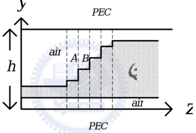
From Fig 2.1, we can observe that we use the staircase approximation to approximate a continuous profile﹒As shown in this figure, such an approximation yields the structure containing three uniform layers for each partition denoted by dash lines﹒Here, we use “region” to represent any partition in the structure, as is region A and region B shown in this figure﹒
When we put the structure into an oversize parallel-plate waveguide, a complete set of modes for each region can be well established, and thus a basic equivalent network will be developed for a junction between any two adjacent regions [8-9]﹒Therefore, for the entire structure, we can cascade these basic unit cells to form an overall equivalent network as is described clearly later with mode matching method in section 2.2﹒Evidently, if we minimize the step size, the approximated structure will approach the practical one﹒Having such an approximation, we can not only simplify the mathematical analysis but also easily interpret the physical phenomenon of the results obtained in the next chapter﹒
ε
PEC PECh
y
z
air air A BFig 2.1 Staircase approximation of an arbitrary continuous profile
2.2 Mode matching method
In this section, we will introduce the procedures of the mode matching method in dealing with the problem described in the previous section﹒First, we want to find the eigen modes for a prescribed layered structure﹒Second, once the eigen modes are determined, the relationship between the mode amplitudes for the two adjacent regions could be determined﹒Finally, we will assess the magnitudes of the voltage and the current for each mode in each region by using the transfer matrices﹒
2.2.1 Transverse-resonance technique
By imposing the condition of transverse resonance along the direction while wave
propagates in the direction, we could set up an equation to solve the propagating
wavenumber and the corresponding mode function
y z z k φ( y)﹒Where kz is defined as eff ε λ π 2
, and ε is the effective dielectric constant﹒A transverse equivalent network for a eff
parallel-plate waveguide containing three uniform layers is shown in the Fig 2.2﹒For TE
mode, the wavenumber and the characteristic impedance along the direction can be
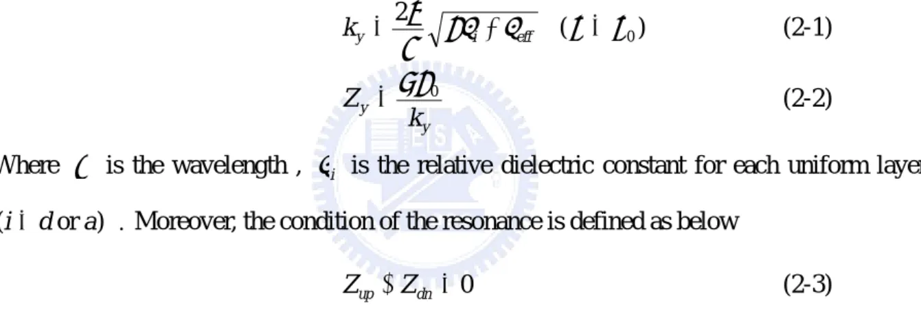
defined as below y eff i y k µε ε λ π − = 2 (µ =µ0) (2-1) y y k Z =ωµ0 (2-2)
Where λ is the wavelength , εi is the relative dielectric constant for each uniform layer
﹒Moreover, the condition of the resonance is defined as below
) or (i=d a 0 = + dn up Z Z (2-3)
Where and are defined as the input impedance looking upward and downward
from the reference plane﹒For a given set of the structure parameters and the operating wavelength, by evaluating equation (2-3), we can easily determine the effective dielectric constants in the structure﹒
up Z Zdn PEC PEC reference plane up Z dn Z ya k ya k yd k yd k 1 d 2 d 3 d 4 d dielectric layer Z Y
Once the roots were found, we could determine the corresponding eigen function,
namely mode function φ( y), distributed in the cross section﹒For TE mode, we can know that
the mode function relates to Ex or Hy and could be written as below
(2-4) ⎩ ⎨ ⎧ + = )) -( sin( ) sin( ) ( , , , , , , , y h k A Z y k A Z y nd yn nd n nd yn p n p yn p n p yn n θ φ layer last for the layer general for
Where n denotes the th mode, represents the layer, and
n p pth An,p θ are the n,p
amplitude and phase of the mode field distributed in the layer, and are
the characteristic impedance and the wavenumber along the direction as described
previously , is the distance between two PEC, and we assume that there are layer in
one region﹒
th
n pth Zyn,p kyn,p
y
h nd
The next step is to find the value of An,pand θ in each layer﹒Because of the n,p
vanishment for the tangential electric field at the surface of the PEC (Ex =0 at y =0 and
), the for the first layer has the form as shown in (2-4) with vanishing
h
y= φn( y) θ ﹒n,1
Furthermore, we set the value of in the first layer to be one﹒By the electromagnetic
boundary condition, that is, the tangential field components must be continuous at the interface between two adjacent dielectric layers, the general solution for the argument
1 , n A p n, θ
and the amplitude An,p could be obtained, written below:
p yn p n p yn yn yn p n k D k D Z Z 1 p , , p , 1 p , p , 1 1 , tan tan( ) + + − + ⎟⎟− ⎠ ⎞ ⎜ ⎜ ⎝ ⎛ + = θ θ (2-5) ) cos( ) cos( 1 , 1 , , , , 1 , + + + + + = p n p p yn p n p p yn p n p n D k D k A A θ θ (2-6)
and the last layer
) cos( ) cos( , 1 , 1 1 , 1 , , nd nd yn nd n nd nd yn nd n nd n d k D k A A = − − − +θ − (2-7)
Where ranges from one to ﹒By progressively matching the field quantity at the
interfaces, we could resolve the unknown and
p nd
s
A' θ's in each region, and thus the mode
function in the transverse plane for each mode can be totally determined﹒
Since the eigen function φn( y) satisfies the Sturm-Liouville differential equation and
the prescribed boundary condition, they should satisfy the orthogonal relation given below:
mn i n i m y w y φ y δ φ()*( ) ( ) ()( ) = (2-8)
Where denotes the region, and represent different mode indices, is the
weighting function corresponding to Sturm-Liouville differential equation﹒For TE mode, the weighting function is defined as below
i ith m n w( y)
1 ) (y =
w (2-9)
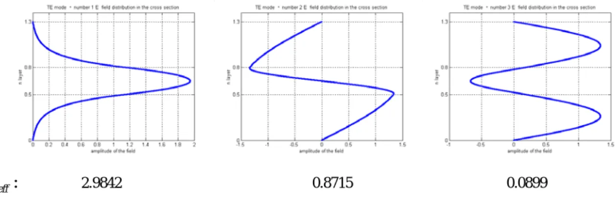
After normalizing each φn( y), we can plot them as shown in the Fig 2.3﹒Here, we
demonstrate a three uniform layers structure and plot the tansverse electric field distribution for the first six modes﹒As shown in this figure, the field, or power density, is guided in the dielectric layer when the corresponding root is greater than unity﹒Such a hind of mode can be regarded as surface wave in dielectric waveguide since the field component is decaying at the surrounding medium, such as air﹒On the contrary, those with effective dielectric constant smaller than unity mean that the wave is propagating in all regions, that is, they exhibit sinusoidal variation in each constituent region﹒
TE P E C P E C Y Z 1 = ε 4 = ε 1 = ε λ 5 . 0 λ 3 . 0 λ 5 . 0 layer three
eff
ε : 2.9842 0.8715 0.0899 Fig 2.3 Transverse fields in a three uniform layers structure for one TE mode
2.2.2 Electromagnetic boundary conditions
After obtaining the eigen modes distributed in a multilayered structure, we shall formulate the boundary value problem along the direction of wave propagation in order to determine the relationship of mode amplitudes at the interface between two adjacent regions﹒ Referring to Fig 2.4 (a), the two regions on the both sides of the discontinuity are characterized by different distributions of the dielectric constant and a junction discontinuity is
at z =z0﹒According to the principle of separation variable, the tangential E and H fields
− 0 z z0+ Z Y − 0 z z0+ ) ( 1 y ε ε2(y) ) (0 ) 1 ( 1 − z V ) (0 ) 1 ( 2 − z V ) (0 ) 2 ( 1 + z V ) ( 0 ) 2 ( 2 + z V ) (0 ) 1 ( 1 − z I ) (0 ) 1 ( 2 − z I ) (0 ) 2 ( 1 + z I ) (0 ) 2 ( 2 + z I 1 region region2 (a) (b)
Fig 2.4 (a) A step discontinuity between two adjacent regions
could be expressed as the superposition of eigen modes in each region, which yields: (2-10) ) ( ) ( () ) ( 1 ) ( z V y E ni ni n i x
∑
φ = = (2-11) ) ( ) ( () ) ( 1 ) ( z I y H ni ni n i y∑
φ = =Where the amplitudes function in direction, and , characterized as voltage and
current waves, satisfy the transmission-line equation along direction as depicted in Fig 2.4
(b), written as: z V 's I 's z ) ( ) ( () () () , ) ( z I Z jk dz z dV i n i n i n z i n =− (2-12) ) ( ) ( () () () , ) ( z V Y jk dz z dI i n i n i n z i n =− (2-13)
Where and consist of both forward and backward propagating waves,
is the propagating wavenumber defined in the section 2.2.1,
) ( ) ( z Vni In(i)(z) kz(,in) ) 1 ( () ) ( i n i n Y Z = is the characteristic
impedance (or admittance) along the z direction defined as below [10] (Appendix 1)
) ( , 0 ) ( i n z i n k Z =ωµ for TE mode (2-14)
By imposing the boundary condition at the interface, the tangential electric and magnetic field
components must be continuous at z =z0﹒From (2-10) and (2-11), we have
(2-15) ) ( ) ( ) ( ) ( (2) (2) 0 1 0 ) 1 ( ) 1 ( 1 2 1 for z V y z V y n n n n n n n n + = − =
∑
∑
φ = φ Ex (2-16) ) ( ) ( ) ( ) ( (2) (2) 0 1 0 ) 1 ( ) 1 ( 1 2 1 for z I y z I y n n n n n n n n + = − =∑
∑
φ = φ HyWhere , and approaches to but not equal to zero, and denote the
number of the modes employed in region1 and region2, respectively﹒By multiplying
z z
equations (2-15) and (2-16) with at the both sides and taking the overlap integral for
the variable from zero to , we have
) ( ) 1 ( y m φ y h ) ( ) ( ) ( ) ( ) ( ) ( (2) 0 (1) (2) 1 ) 1 ( ) 1 ( 0 ) 1 ( 1 2 1 y y z V y y z V n m n n n n m n n n φ φ φ φ + = − =
∑
∑
= (2-17) ) ( ) ( ) ( ) ( ) ( ) ( (2) 0 (1) (2) 1 ) 1 ( ) 1 ( 0 ) 1 ( 1 2 1 y y z I y y z I n m n n n n m n n n φ φ φ φ + = − =∑
∑
= (2-18)By invoking the orthogonal relation for the eigen mode, the above equations can be written as: (2-19) mn n n n m z V z V ( ) (2)( 0)γ 1 0 ) 1 ( 2 + = − =
∑
(2-20) mn n n n m z I z I ( ) (2)( 0)γ 1 0 ) 1 ( 2 + = − =∑
) ( ) ( (2) ) 1 ( y y n m mn φ φ γ = (2-21)Where ranges from one to , runs from one to , represents the coupling
between and mode in respective region﹒The above linear system of homogeneous
equations can be rewritten in the vector-matrix form, given below:
m n1 n n2 γmn
th
m nth
V1 =ℜV2 (2-22)
I1 =ℜI2 (2-23)
Where is defined as coupling matrix with its element , and are the
voltage and current vectors with their mode amplitude filling in the entries﹒By multiplying
equations (2-15) and (2-16) with at both sides and taking the overlap integral
incorporated with the orthogonal relation, we obtain the similar matrix equations given below:
ℜ γmn V 's I 's ) ( ) 2 ( y m φ V2 =ℜTV1 (2-24)
1 2 I
I =ℜT (2-25)
Where the superscript T denotes the transpose of the coupling matrix ℜ ﹒
After obtaining the coupling matrix between any two adjacent regions, we could further check the accuracy of these matrices [3]﹒If the coupling matrix is not accurate, the condition of power conservation will not be present and some errors will occur﹒ Substituting (2-24) into (2-22) or (2-25) into (2-23), we have the unitary condition:
ℜℜT = I (2-26)
Where I is the identity matrix﹒In general, (2-26) may be considered as an criterion to see
whether the coupling matrices are accurate or not in the numerical computation﹒
2.2.3 Input-output relation
From the previous section, we have obtained the coupling matrix between two adjacent regions, each of which contains multiple uniform layers﹒In this section, we will introduce a procedure to deal with the wave propagation through multiple discontinuities by using the input-output relation at the discontinuity and wave transition in a uniform waveguide﹒Once the relationship described previously is obtained, we have a good position in figuring out the field components everywhere in the structure﹒
Fig 2.5 (a) shows a parallel-plate waveguide filled with nonhomogeneous dielectric medium﹒Since the dielectric medium is piecewise constant, we could partition them into three
interfaces characterizing the discontinuities of the structure, which are and , respectively﹒Based on the mode matching method described in the previous section , the transmission-line network in the uniform waveguide and the transformer bank at the discontinuities could be drawn as depicted in Fig 2.5(b)﹒
1 − =zi z z= zi
Z
Y
1
-i
region
region
i
region
i
+
1
1 − i
t
t
i 1 + it
)
(
) 1 (y
i−ε
ε
(i)(
y
)
(
)
) 1 (y
i+ε
)
(a
PEC
PEC
− −1 i zz
i+−1z
i−z
i+ ) ( 1 ) ( 1 + − i i z V ()( ) 1 − i i z V ) ( 1 ) ( 1 + − i i z I ()( ) 1 − i i z I ) ( 1 ) ( + − i i n z V i ) ( 1 ) ( + − i i n z I i ) ( ) ( − i i n z V i ) ( ) ( − i i n z I i)
(b
) ( 1 ) 1 ( 1 − − − i i z V ) ( 1 ) 1 ( 1 − − − i i z I ) ( 1 ) 1 ( 1 − − − − i i n z Vi ) ( 1 ) 1 ( 1 − − − − i i n z Ii ) ( ) 1 ( 1 + + i i z V ) ( ) 1 ( 1 + + i i z I ) ( ) 1 ( 1 + + + i i n z Vi ) ( ) 1 ( 1 + + + i i n z Ii − −1 i zz
i+−1z
i−z
i+Fig 2.5 Equivalent network for a staircase structure (a) Three regions
(b) Equivalent network
Here, we assume that the structure infinitely extends at the right hand side of Fig 2.5 (a),
or the input impedance of each mode in the region is known﹒Thus, the input
impedance matrix contains each mode in that region is assumed to be ﹒Where
is a full matrix, which may include the mutual coupling effect due to waveguide modes in the present of discontinuities﹒
th i+1 ) ( + + i in z Z ) ( + + i in z Z
further transfer it from the right hand side of the interface, to the left one﹒Since the
voltage and current waves in the region i and
+ = zi
z
1 +
i satisfy the relationship given in
equation (2-22)~(2-25), we could obtain the input impedance matrix looking seen into the
region at , which is given below:
th i+1 z=zi− (2-27) T in in Z Z− =ℜ +ℜ
In the previous section, we have transformed the input impedance matrix from the output region to the input region through a discontinuity by using the input-output relation of that discontinuity﹒Thus, in the next step, we should tackle the problem of wave transition in a
uniform waveguide (in the region )﹒There are two problems to be handled, which are the
input impedance matrix looking seen into the interface at and the transform matrix
for the electric and magnetic fields from the output to the input interfaces of the finite section
of waveguide ( region)﹒ th i + − = zi 1 z th i
In a uniform waveguide, the voltage and current waves for each mode could be grouped into the vectors, which are given below:
{
Vn z}
n N z V K 1 ) ( ) ( = = (2-28){ }
In z n N z I K 1 ) ( ) ( = = (2-29)For a finite length of transmission line, the voltage and current waves contain those of forward and backward propagation ones, which could be written as:
b e a e z V( )= −jκz + jκz (2-30)
[
e a e b]
Y z I( )= −jκz − jκz (2-31)Where the matrix e−jκz is a diagonal matrix with its diagonal element representing the
consisting of each forward and backward propagating modes﹒Besides, is the admittance matrix, each element representing the characteristic admittance of mode in the transmission line﹒
Y
Once the impedance matrix at the output of the transmission line is determined, we could further obtain the relationship between the forward and backward propagating amplitudes vectors a and b both at z= zi− and z =zi+−1, which is given below:
(2-32) ) ( ) (ZinYi I 1 ZinYi I out = + − Γ − − − i i j t out t j e e− κ Γ − κ = Γ (2-33)
Where Γout and Γ represent the reflection matrices at and ﹒Then, the
input impedance matrix looking to the right at is determined by the impedance
transform technique as:
− =zi z z= zi+−1 + − =zi 1 z (2-34) i in I I Z Z 1 ) )( ( − + = +Γ −Γ
From the mention above, the input-output relation for waves at the discontinuities and in each uniform waveguide are determined, we could sufficiently employ the equations (2-27),(2-32)~(2-34) to calculate the input impedance matrix from the last region to the first
region﹒Besides, the electric field components in each section could also be obtained by using
the transfer matrices﹒In detail speaking, if the input impedance matrix at the input interface is
given as , thus we have the relationship between the forward and backward waves,
which are written as : in Z b=Γina (2-35) (2-36) ) ( ) ( 1 1 1 I Z Y I Y Zin in in = + − Γ −
Where the Γin represents the reflection matrix at the input surface, a and b are those
determined, the reflected amplitudes for each mode shall be totally understood in equation (2-35)﹒Thus, the voltage at the input surface could be given below:
a I
V(0)=( +Γin) (2-37)
Moreover, the voltage vector at the output surface could be obtained by the transfer matrix of
each finite section and we assume that there are N basic units, which yields:
) 0 ( ) ( ) ( 1 V t V N i i i ⎥ ⎦ ⎤ ⎢ ⎣ ⎡ Τ =
∏
= l (2-38)Where V(l) is the voltage vector at the output surface (z=l) , Τ is the transfer matrix i
consists of a step discontinuity and a uniform waveguide of thickness ﹒Moreover, the input-output relation in a uniform waveguide is given below (Appendix 2):
i t ) ( ) ( ) ( ) (zi− = I+Γout e−j t I+Γ −1V zi+−1 V κii (2-39)
In a word, by using the input-output relations for the discontinuity and uniform transmission line, we could simply figure out the electric field everywhere﹒Thus, the scattering characteristics of waveguide mode by an arbitrary nonhomogeneous structure could be understood by the procedures given in the previous paragraph﹒
After determining the voltage and the current vectors in the input and output regions, we must check the principle of power conservation﹒This is the criterion to see whether the voltage and the current matrices are accurate or not﹒If the power is not conserved, the solution to this problem is not accurate﹒By using the Poynting theorem, the formulation of the power conservation is shown as below:
⎥⎦ ⎤ ⎢⎣ ⎡ = ⎥⎦ ⎤ ⎢⎣ ⎡ − ⎥⎦ ⎤ ⎢⎣ ⎡ ∗ = ∗ = ∗ =
∑
∑
∑
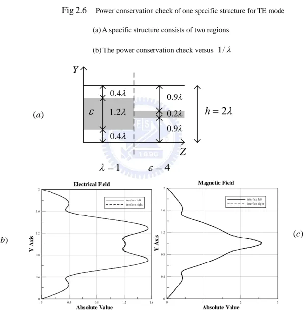
( ) 0 2 ) ( , 1 ) 1 ( 0 2 ) 1 ( , 1 ) 1 ( 0 2 ) 1 ( , 1 Re Re Re 1 1 M M t n n n r n n n in n n n Y V Y V Y V M (2-40)From the equation above, we can observe that the incident real power is equal to the sum of reflected and transmitted powers﹒ In a word, the two factors affecting the power conservation are: (1) the eigen function in the transverse direction should form a complete set, and (2) the dispersion roots should be figured out rigorously﹒Fig 2.6 depicts the power conservation check versus a range of the wavelength for a specific structure﹒As shown in the figure, the power conservation is very good for a wide frequency band﹒
After the power conservation is checked successfully, the next step is to check whether the tangential electric and the magnetic fields are continuous at the discontinuity﹒We have plotted the tangential electric and magnetic components in the respective region at the interface﹒Fig 2.7 (a) is the structural configuration and parameters of a junction discontinuity, wherein the two dielectric stabs have different thickness, however, they are infinitely extending﹒Fig 2.7 (b) and (c) depict the tangential electric and magnetic field components, respectively﹒The two figures exhibit the good agreement in the field continuity and prove the accuracy of the computational method in this thesis﹒
λ 4 . 0 λ 4 . 0 λ 2 . 1 λ 9 . 0 λ 9 . 0 λ 2 . 0
h
=
2
λ
Z
Y
ε
1
~
5
:
λ
ε
=
4
) (a) (b
Fig 2.6 Power conservation check of one specific structure for TE mode (a) A specific structure consists of two regions
(b) The power conservation check versus 1/λ
λ 4 . 0 λ 4 . 0 λ 2 . 1 λ 9 . 0 λ 9 . 0 λ 2 . 0
h
=
2
λ
Z
Y
1
=
λ
ε
4
=
ε
) (a 0 0.4 0.8 1.2 1.6 Absolute Value 0 0.4 0.8 1.2 1.6 2 Y A xi s interface left interface right Electrical Field 0 1 2 3 Absolute Value 0 0.4 0.8 1.2 1.6 2 Y A xi s interface left interface right Magnetic Field ) (c ) (bFig 2.7 Tangential E and H fields on the both sides of the interface for TE mode (a) A specific structure consists of two regions
(b) The absolute value of the tangential electrical fields on the both sides at the junction discontinuity (c) The absolute value of the tangential magnetic fields on the both sides at the junction discontinuity
Chapter 3
Numerical Results and Discussions
In this chapter, we will illustrate several typical transition structures which are often used in the optical circuits design﹒As is found in these figures, we plot the normalized power transmission versus a certain range of the transition length, and thus we can realize how long the transition length will be with the desired efficiency﹒Moreover, the power conservation is between 0.99990 and 1.00009 for most of the computing points﹒Finally, we will interpret the phenomenon existing in these figures with physical concepts, such that we can make sure the results we obtained are reasonable and acceptable﹒
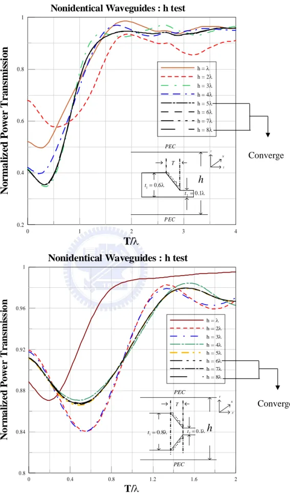
From Fig 3.2, we can easily observe that the results for these two cases will converge
while , where is the thickness of the most thickest region in the structure﹒
Therefore, in the following analysis, we separate the distance of the parallel-plate waveguide
larger than to approximate the practical situation﹒Furthermore, for a certain
thick t h>7 tthick thick t 8 T , we
also test how many steps or basic units are needed to approximate the continuous profile of
the transition structure﹒As is found in Fig 3.3, the number of the steps for a certain is at
least
T
λ
T
×
4 to receive the convergent result﹒
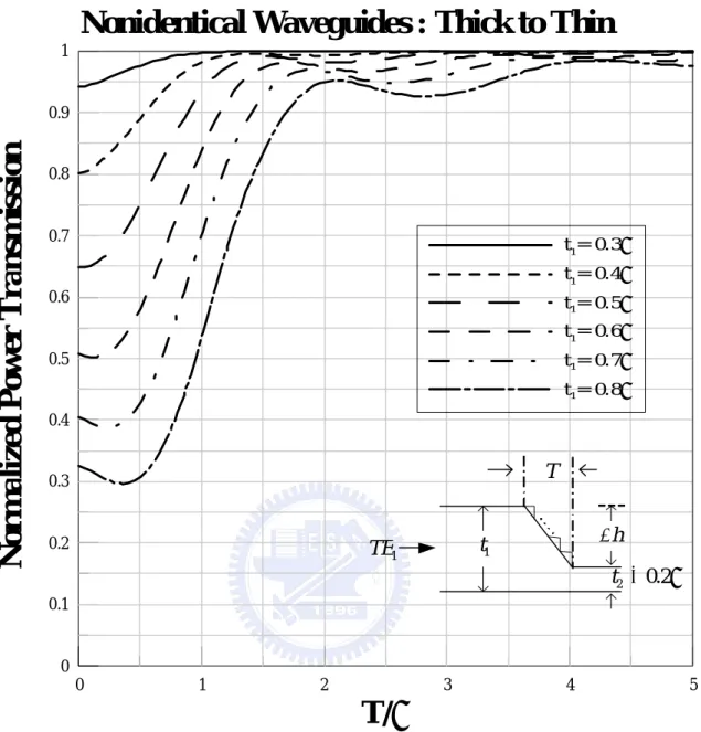
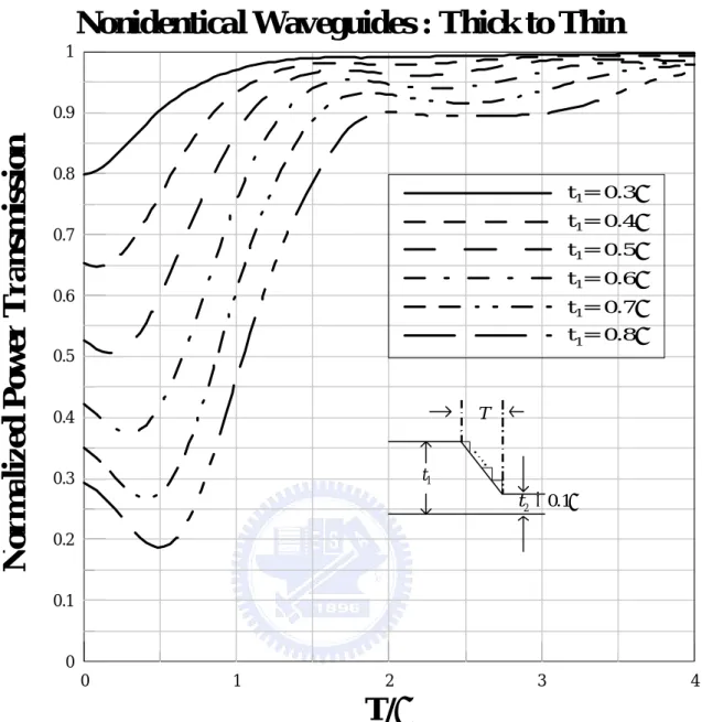
waveguides with different thickness as shown in Fig 3.4﹒The first surface wave mode ( ) is fed from thick waveguide into thin one which is placed on the bottom of the structure﹒ Moreover, there is only one surface wave mode existing in the thin waveguide﹒Here, we
illustrate six different value of and
1 TE
1
t ∆ represents the distance between and ﹒We h
observe that as is greater, a longer transition length (T) is needed to transmit over 95%
incident power successfully, such as
1 t t2 h ∆ λ 75 . 0 >
T for t1 =0.4λ and T >3.5λ for
λ
8 . 0
1 =
t ﹒The interpretation is that as h∆ is increasing, for a fixed number of steps ( ),
the variation of the characteristic impedance (
c
N
Z
∆ ) along the direction between adjacent
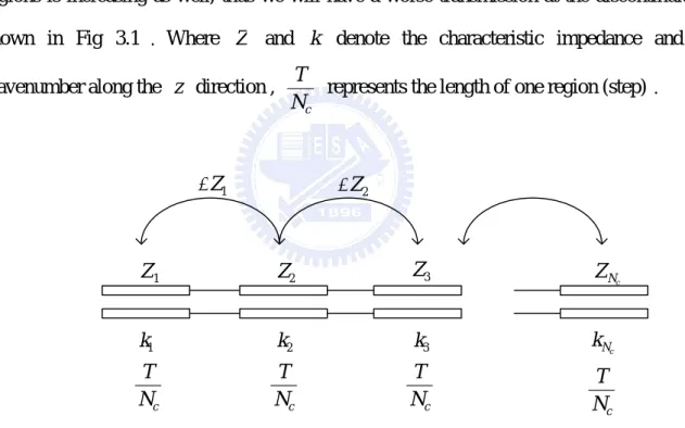
regions is increasing as well, thus we will have a worse transmission at the discontinuity as shown in Fig 3.1 ﹒ Where
z
Z and denote the characteristic impedance and the
wavenumber along the direction ,
k
z
c
N T
represents the length of one region (step)﹒
c N k c N T c N Z K K 1 Z Z2 1 k k2 k3 3 Z c N T 1 Z ∆ ∆Z2 c N T c N T
Fig 3.1 The equivalent network of the transition structure
Fig 3.5 shows the same condition with Fig 3.4 for greater ∆ for all cases﹒With the h
same interpretation above, as is expected, the transmission is worse than in Fig 3.4 and a
longer T is needed to receive the same desired transmission efficiency﹒
structure﹒For all cases, we can observe that the transmission is better than previous figure﹒
The interpretation is that, as the thin waveguide is closer to the central of the structure, ∆Z
is smaller between adjacent regions, such that the transmission is better at the discontinuity﹒
Fig 3.7 depicts another case of transition for a step discontinuity between two uniform waveguides﹒Compared with Fig 3.4, we can observe that the transmission in Fig 3.7 is much
better while is fed from thin waveguide into thick one﹒The interpretation is that there
are more than one surface wave mode existing in the thick waveguide, and thus the magnitude of coupling is much stronger at the discontinuity﹒Fig 3.8 depicts the same condition with Fig
3.7 for a smaller ﹒As is expected, with larger
1 TE
1
t ∆ for all cases, the transmission is worse h
than in Fig 3.7 and the interpretation has been mentioned in the third paragraph﹒
Fig 3.9 shows the transmission characteristics of bended waveguides with two different cases﹒The profile of the transition region is formulated by the following equation:
λ a T x y= )× 91024 . 0 tanh( (4-1)
Where T represents the transition length, a represents the distance between the two λ
waveguides axes﹒Obviously observed from (a) and (b), the transmission is worse while the distance between the two waveguides axes is longer﹒Another phenomenon is that the transmission of the thick case is better than the thin one﹒The interpretation is that the number of the surface wave modes in the thick case is more than the thin one, thus the coupling is stronger at the discontinuity and a better transmission will be obtained﹒
Fig 3.10 shows the transmission characteristics of another bended type waveguide with
and t=0.35λ, respectively﹒The profile is symmetric and the left half of the transition region is formulated by the following equation:
λ × =tanh( ) T x y (4-2)
Where T and λ represent the transition length and the operating wavelength﹒Observed
from this figure, with the same interpretation mentioned in the previous paragraph, the transmission is better for the thick case than for the thin one﹒
Fig 3.11 shows the transmission characteristics of the perturbed waveguide with three different cases﹒From this figure, we can observe that as the lower bound of the transition region is more flat, the transmission is better﹒
Fig 3.12 shows the transmission characteristics of a crack waveguide with three
different cases﹒From this figure, we can observe that , when T =0, the transmission is worse
while the length of S is longer, such as Pt =0.58 for S =0.6λ and Pt =0.52 for
λ
2 . 1 =
S ﹒As is found, the transition length is at least 3 for over 95% power can be λ
transmitted successfully for these three cases﹒Fig 3.13 shows the same condition with Fig 3.12 for a deeper crack waveguide﹒As is expected, the transmission is worse and the transition length is longer than Fig 3.12 for the same desired transmission efficiency﹒An interesting phenomenon can also be observed from Fig 3.12 and Fig 3.13 that, while the transition length is greater than about 1.5λ, the curves in both figures will get very closely to each other﹒The interpretation of such a phenomenon is listed as below﹒First, we can divide the crack waveguide in Fig 3.12 into two half parts, the left half side is the same with the Fig 3.4, and the right half side is the same with the Fig 3.7﹒From Fig 3.7, we can easily observe
that, for t2 =0.8λ, over 99% power can be transmitted while the transition length is greater than 1.5λ﹒Therefore, while T >1.5λ, the curves in Fig 3.12 for all cases are dominated by Fig 3.4, such that these different cases can be seen as the similar ones﹒
0 1 2 3 4
T/
λ
0.2 0.4 0.6 0.8 1No
rm
a
li
z
ed
P
o
w
er T
ra
ns
m
is
si
o
n
h = λ h = 2λ h = 3λ h = 4λ h = 5 h = 6 λ λ h = 7λ h = 8λNonidentical Waveguides : h test
λ 1 . 0 2= t T λ 6 . 0 1= t
h
Y Z X Converge PEC P EC 0 0.4 0.8 1.2 1.6 2 T/λ 0.8 0.84 0.88 0.92 0.96 1 No rm a li z ed P o w er T ra n sm is si o n h = λ h = 2λ h = 3λ h = 4λ h = 5λ h = 6λ h = 7λ h = 8λNonidentical Waveguides : h test
λ 1 . 0 2= t T λ 8 . 0 1= t
h
Y Z X PEC PEC ConvergeFig 3.2 Test the separation distance of theparallel-plate waveguide to pursue the convergent result
0 1 2 3 4 5
T/
λ
0.1 0.2 0.3 0.4 0.5 0.6 0.7 0.8 0.9 1N
o
rm
a
li
zed P
o
w
er
T
r
a
n
sm
issi
o
n
Nc = 4 Nc = 5 Nc = 8 Nc = 12 Nc = 16 Nc = 20 Nc = 24 Nc = 28 Nc = 32Nonidentical Waveguides : staircase test
λ 2 . 0 2 = t T λ 8 . 0 1 = t h =7λ Y Z X PE C PEC c N
0 1 2 3 4 5
T/
λ
0 0.1 0.2 0.3 0.4 0.5 0.6 0.7 0.8 0.9 1No
rm
a
li
zed P
o
w
er T
ra
ns
m
is
si
o
n
t1= 0.3λ t1= 0.4λ t1= 0.5λ t1= 0.6λ t1= 0.7λ t1= 0.8λNonidentical Waveguides : Thick to Thin
λ 2 . 0 2 = t T 1 t ∆h 1 TE
Fig 3.4 Transmission through two uniform waveguides with different thickness: Thick to Thin The thin waveguide is placed on the bottom of the structure﹒t2 = 0.2λ
0 1 2 3 4
T/
λ
0 0.1 0.2 0.3 0.4 0.5 0.6 0.7 0.8 0.9 1N
o
rm
a
li
zed
P
o
we
r T
ra
n
sm
issi
o
n
t1= 0.3λ t1= 0.4λ t1= 0.5λ t1= 0.6λ t1= 0.7λ t1= 0.8λNonidentical Waveguides : Thick to Thin
λ 1 . 0 2 = t T 1 t
Fig 3.5 Transmission through two uniform waveguides with different thickness: Thick to Thin The thin waveguide is placed on the bottom of the structure﹒t2 =0.1λ
0 0.5 1 1.5 2
T/
λ
0.8 0.82 0.84 0.86 0.88 0.9 0.92 0.94 0.96 0.98 1N
o
rm
a
li
zed
P
o
w
e
r T
ra
n
sm
is
sio
n
t1= 0.3λ t1= 0.4λ t1= 0.5λ t1= 0.6λ t1= 0.7λ t1= 0.8λNonidentical Waveguides : Thick to Thin
λ 1 . 0 2 = t T 1 t
Fig 3.6 Transmission through two uniform waveguides with different thickness: Thick to Thin The thin waveguide is placed in the central of the structure﹒t2 = 0.1λ
0 1 2 3 4
T/
λ
0.96 0.97 0.98 0.99 1No
rm
a
li
zed P
o
w
er T
ra
ns
m
is
sio
n
t2= 0.3λ t2= 0.4λ t2= 0.5λ t2= 0.6λ t2= 0.7λ t2= 0.8λNonidentical Waveguides : Thin to Thick
λ 2 . 0 1 = t T 2 t
Fig 3.7 Transmission through two uniform waveguides with different thickness: Thin to Thick The thin waveguide is placed on the bottom of the structure﹒t1=0.2λ
0 1 2 3 4
T/
λ
0.8 0.84 0.88 0.92 0.96 1No
rm
a
li
zed P
o
w
er T
ra
ns
m
is
sio
n
t2= 0.3λ t2= 0.4λ t2= 0.5λ t2= 0.6λ t2= 0.7λ t2= 0.8λNonidentical Waveguides : Thin to Thick
λ 1 . 0 1= t T 2 t ∆h
Fig 3.8 Transmission through two uniform waveguides with different thickness: Thin to Thick The thin waveguide is placed on the bottom of the structure﹒t1 =0.1λ
0 1 2 3 4 5 6 T/λ 0 0.1 0.2 0.3 0.4 0.5 0.6 0.7 0.8 0.9 1 No r m a li zed P o w e r Tra n sm is si o n t = 0.1λ transmission t = 0.3λ transmission Bended Waveguides-type A t
T
X Yλ
0 1 2 3 4 5 6 7 8 9 10 11 12 T/λ 0 0.1 0.2 0.3 0.4 0.5 0.6 0.7 0.8 0.9 1 Nor m alized Pow er Tran sm ission t = 0.1λ transmission t = 0.3λ transmission Bended Waveguides-type A tT
X Y λ 2Fig 3.9 Transmission efficiencies of bended waveguides (type A)
with two different thickness
TE mode, Pin=1, ε=4, aλ T x y= )× 91024 . 0 tanh( (a) a=1 (b) a=2
0 1 2 3 4 5 6 7 8 9 10
T/
λ
0 0.1 0.2 0.3 0.4 0.5 0.6 0.7 0.8 0.9 1N
o
r
m
a
liz
e
d
P
o
w
e
r
T
r
a
n
sm
is
si
o
n
t = 0.1λ t = 0.35λBended Waveguides-type B
x y t TFig 3.10 Transmission efficiency of a bended waveguide (type B)
with two different thickness
TE mode, Pin=1, ε=4, =tanh( )×λ
T x y
0 1 2 3 4 5 6 7 8
T/
λ
0 0.1 0.2 0.3 0.4 0.5 0.6 0.7 0.8 0.9 1Normalized Powe
r Trnasmission
Perturbed Waveguides
λ 3 . 0 λ 42 . 0 T 0 . 4 = ε λ 2 . 0 λ 3 . 0 λ 5 . 0 T 0 . 4 = ε λ 12 . 0 λ 3 . 0 λ 62 . 0 T 0 . 4 = εFig 3.11 Comparison between three perturbed waveguides of different types
0 0.5 1 1.5 2 2.5 3 3.5 4 4.5 5
T/
λ
0 0.1 0.2 0.3 0.4 0.5 0.6 0.7 0.8 0.9 1No
rma
li
zed
P
o
w
er
T
r
a
n
sm
issio
n
S = 0 S = 0.6λ S = 1.2λCrack Waveguides
λ 8 . 0 λ 2 . 0 T s T 4 = εFig 3.12 Transmission through a crack with three different types
0 0.5 1 1.5 2 2.5 3 3.5 4 4.5 5 5.5 6
T/
λ
0 0.1 0.2 0.3 0.4 0.5 0.6 0.7 0.8 0.9 1No
rm
a
liz
ed
P
o
w
er
T
ra
ns
m
is
si
o
n
S = 0 S = 0.6λ S = 1.2λCrack Waveguide
λ 8 . 0 λ 1 . 0 T s T 4 = εFig 3.13 Transmission through a crack with three different types A deeper case than Fig 3.12
Chapter 4
Conclusion
To sum up, we have formulated a systematic way to analyze any type of the transition
structure by using the staircase approximation and the mode matching method﹒In the process of the analysis, by separating the distance of the parallel-plate waveguide far enough and adopting sufficient number of steps, we can receive the corresponding results which are expected approaching the practical situation﹒
From the previous chapter, we have surveyed a large class of transition structures while the first surface wave mode is incident form the left﹒With the extensive numerical results, we can easily observe that we need a longer transition length to receive the desired transmission efficiency while the variation of the structure is getting greater﹒Moreover, as the number of the surface wave modes in the dielectric waveguide is greater, the coupling is stronger at the discontinuity﹒Above all, from these figures, we have developed a useful criterion to design the transition structures with the desired transmission efficiency﹒
Appendix
Appendix 1: The characteristic impedance along the Z direction
for
TE
mode
From reference [10], we can receive the relationship between the transverse E and H fields as shown in below: ) ) , ( ( ) ) ( 1 ( ) , ( 2 0 0 z y x h y k y x e Z i t t i i i ⋅ × ∇ + = ε ωµ κ (1) )) , ( ( ) ) ( 1 )( ( ) , ( 2 0 0 0 z e x y y k y y x h Y i t t i i i ⋅ × ∇ + = ε ε ωε κ (2)
Where i represents the th mode,
i ei(x,y) and hi(x,y) represent the transverse
distribution of the transverse electric and magnetic components﹒For TE mode, the transverse field components are listed as below:
(3) ) ( ) (yV z Exi =φi i (4) ) ( ) (y I z Hyi =φi i ) ( ) ( 1 0 z V dy y d j H i i zi φ ωµ − = (5)
Substituting (3)~(5) into (2), we can receive:
⋅ ∂ ∂ + ∂ ∂ ∂ + ∂ ∂ ∂ + ∂ ∂ + + = )] ) ( ) ( ( ) )[( ( ) ( 2 0 0 0 2 2 0 2 0 2 0 0 2 0 2 2 0 0 0 0 0 0 y y k y y x y x x y k y y x x x y y x x y y y Yi i i φ ωε ε ε ε κ ) ) ( (z0×φi y x0 (6)
From the equation above, we have two relations: 1. κiZiφi (y)x0 =ωµφi (y)x0 2. )] ) ( ) ( ( ) ) ( )[( ( ) ( 2 0 0 2 2 0 0 0 y y k y y y y y y y Y i i i i i ε φ φ ε ωε φ κ ∂ ∂ + =
From relation 1, we can determine the characteristic impedance for TE mode along the direction as below: z i i Z κ ωµ = (7)
Appendix 2: The input-output relation in the uniform waveguide
Z Y 1 -iregion regioni regioni+1
1 − i t ti 1 + i t ) ( ) 1 ( y i− ε ε(i)(y) ( ) ) 1 ( y i+ ε ) (a PEC PEC − −1 i z zi+−1 zi− zi+ ) ( 1 ) ( 1 + − i i z V ()( ) 1 − i i z V ) ( 1 ) ( 1 + − i i z I ()( ) 1 − i i z I ) ( 1 ) ( + − i i n z Vi ) ( 1 ) ( + − i i n z I i ) ( ) ( − i i n z V i ) ( ) ( − i i n z I i ) (b ) ( 1 ) 1 ( 1 − − − i i z V ) ( 1 ) 1 ( 1 − − − i i z I ) ( 1 ) 1 ( 1 − − − − i i n z Vi ) ( 1 ) 1 ( 1 − − − − i i n z Ii ) ( ) 1 ( 1 + + i i z V ) ( ) 1 ( 1 + + i i z I ) ( ) 1 ( 1 + + + i i n z Vi ) ( ) 1 ( 1 + + + i i n z Ii − −1 i z zi+−1 − i z zi+
From this figure, we assume that we have received the voltage vector, V(zi+−1), at the
interface, and then we must implement several steps to find the voltage vector at the next interface in the same region﹒
th
i 1−
First of all, the expressions of the forward amplitude vector, a , atz =zi+−1 is given by:
( ) 1 ( +1) − − Γ + = I V zi a (1)
Where Γ is the reflection coefficient matrix atz= zi+−1, I is the unitary matrix﹒As we
know, Γ can be expressed as follows:
i i j t out t j e e− κ Γ − κ = Γ (2)
Where Γout is the reflection coefficient matrix at z=zi−﹒Moreover, the voltage vector at
− =zi
z , V(zi−), can be expressed as follows:
V z e j tia ej ti a i = + Γ − − κ κ ) ( (3)
Substitute (2) into (3), we have: a e I z V j ti out i κ − − = +Γ ) ( ) ( (4)
Finally, we substitute (1) into (4), then we have:
) ( ) ( ) ( ) (zi− = I +Γout e−j t I +Γ −1V zi+−1 V κi (5)
From equation (5), we have successfully received V(zi−) by transferring V(zi+−1) and the input-output relation in a uniform waveguide is defined as:
1 ) ( ) (I +Γ e−j ti I+Γ − out κ (6)
Bibliography
[1] Song-Tsuen Peng; Oliner, A.A. ”Guidance and Leakage Properties of a Class of
Open Dielectric Waveguides: Part I--Mathematical Formulations” Microwave
Theory and Techniques, IEEE Transactions on , Volume: 29 , Issue: 9 , Sep 1981 ,
Pages:843 - 855
[2] Oliner, A.A.; Song-Tsuen Peng; Ting-Ih Hsu; Sanchez, A. ”Guidance and Leakage
Properties of a Class of Open Dielectric Waveguides: Part II--New Physical Effects” Microwave Theory and Techniques, IEEE Transactions on , Volume: 29 , Issue:
9 , Sep 1981 , Pages:855 – 869
[3] Ruey Bing Hwang ”The improvement of tri-plate line performance by using
corrugated transitions” Electromagnetic Compatibility, IEEE Transactions
on , Volume: 42 , Issue: 4 , Nov. 2000 , Pages:314 - 325
[4] Brooke, G.H.; Kharadly, M.M.Z ”Scattering by Abrupt Discontinuities on Planar
Dielectric Waveguides” Microwave Theory and Techniques, IEEE Transactions
on , Volume: 82 , Issue: 5 , May 1982 , Pages:760 – 770
[5] Shigesawa, H.; Tsuji, M. ”Mode Propagation through a Step Discontinuity in
Dielectric Planar Waveguide” Microwave Theory and Techniques, IEEE Transactions
on , Volume: 34 , Issue: 2 , Feb 1986 , Pages:205 – 212
[6] Lewin ”Radiation from Curved Dielectric Slabs and Fibers” Microwave Theory and
Techniques, IEEE Transactions on , Volume: 22 , Issue: 7 , Jul 1974 , Pages:718 – 727
[7] Peng, S.T. ”Transitions in open millimetre-wave waveguides” Microwaves,
Antennas and Propagation [see also IEE Proceedings-Microwaves, Antennas and Propagation], IEE Proceedings H , Volume: 136 , Issue: 6 , Dec. 1989 Pages:487 – 491
[8] Shanjio Xu; Peng, S.T.; Schwering, F.K. ”Effect of transition waveguides on
dielectric waveguide directional couplers” Microwave Theory and Techniques,
[9] Xu, S.-J. ”Dielectric-waveguide branching directional coupler” Microwaves, Antennas and Propagation , IEE Proceedings H , Volume: 135 , Issue: 4 , Aug. 1988 , Pages:282 - 284
[10] Altschuler, H.M.; Goldstone, L.O. ”On Network Representations of Certain
Obstacles in Waveguide Regions” Microwave Theory and Techniques, IEEE