856 IEEE TRANSACTIONS ON ELECTRON DEVICES, VOL 42. NO. 5 , MAY 1995
A
Novel Extraction Technique for the Effective
Channel Length
of
MOSFET Devices
Hsin-Hsien
Li,
Student Member, IEEE, and Ching-Yuan Wu, Member, IEEEAbstract-A novel method using the charge pumping technique
for extracting the effective channel length of MOSFET devices is presented, in which the effective area approach is used and the edges of the area are defined clearly. It is shown that the extracted effective channel length is independent of the measuring biases and the proposed new method is simple, accurate, and reliable, as compared to those using the I-V method. With the knowledge of the device dopant profiles, the extracted channel length with 0.01
pm accuracy can he achieved. Moreover, the proposed method is applicable to either n- or p-channel, conventional or LDD, surface or buried channel MOSFET’s.
NOMENCLATURE V F B Flat band voltage.
T o , Gate oxide thickness.
V G ~ ( V ~ ~ ) T H ( T L )
Lmaslc ( L e f f ) Drawn (effective) channel length. High (low) voltage of gate pulses. Duration time of high (low) gate bias per cycle.
T /
Gate voltage. Threshold voltage. Drain (source) voltage.
Critical hole concentration at the effective area edges.
Surface hole concentration. Hole capture (emission) rate. Electron capture (emission) rate. Thermal velocity.
Hole (electron) capture cross section. Intrinsic Fermi energy.
Hole (electron) quasi-Fermi energy. Intrinsic carrier concentration. Occupied interface-trap density. Interface-trap density.
Energy of conduction (valence) band edge. Elementary charge.
Effective channel width. Frequency of gate pulses. Period of gate pulses.
Lateral position along the channel.
Distance between metallurgical junction and effective area edge.
Manuscript received March IO, 1994; revised July 18, 1994. The review of this paper was arranged by Associate Editor J. R. Hauser. This work was supported by the National Science Council, Taiwan, ROC, under Contract
The authors are with the Advanced Semiconductor Device Research Labora- tory and the Institute of Electronics, National Chiao-Tung University, Hsinchu, Taiwan, ROC.
NSC-82-0404-E009-2 16.
IEEE Log Number 9410473.
Iv Charge pumping current.
Icp, nLaI Maximum charge pumping current per unit length related to the gate waveform along the channel.
S R ( S F ) Absolute slope of the rise (fall) edges of gate pulses.
D,t Average interface trap density. k B Boltzmann constant.
T Absolute temperature.
t,, e ( t r m , p )
Time for trapped electrons (holes) to emit before recombination.I. INTRODUCTION
S the channel length of MOSFET’s becomes shorter,
A
the short-channel effects on the device characteristics become very important. In general, the deviations of the channel length from the mask length may come from the errors due to the lithographic process and the lateral diffusion of source/drain islands. The effective channel length of a MOSFET is often defined as the surface spacing between the metallurgical source/drain junction, which may differ from the electrical channel length, depending on the device structure of MOSFET’s. In order to accurately characterize the I-V and C-V characteristics of an experimental short channel-length MOSFET, accurate determination of the effective channel length becomes very important.Up to now, many efforts have been made to find a simple and accurate method to measure the effective channel length of a MOSFET device [1]-[lo]. Most of them are based on the turn-on I-V characteristics of MOSFET’s operated at low drain bias 111-161, in which the method proposed by Terada er al. [ l ] has been used widely and is called the resistance method. However, this method and its modifications [2]-[6] become inaccurate for lightly doped drain (LDD), double diffused drain (DDD) or short-channel MOSFET devices, due to the variations of the sourceldrain resistances with the gate voltage and the threshold voltage with the channel length. To avoid these problems, some other approaches have been proposed, based on the characteristics of the parasitic bipolar transistor 171, the saturation velocity 181, the punch- through voltage [9], and the gate capacitance [lo]. However, the accuracy of the parasitic bipolar transistor and punch- through voltage methods becomes questionable for practical MOS devices with nonuniform substrate dopant profile. For the gate capacitance method, the source/drain overlapping and fringing capacitances are much larger than the intrinsic gate capacitance using the measured C-V data, the errors produced
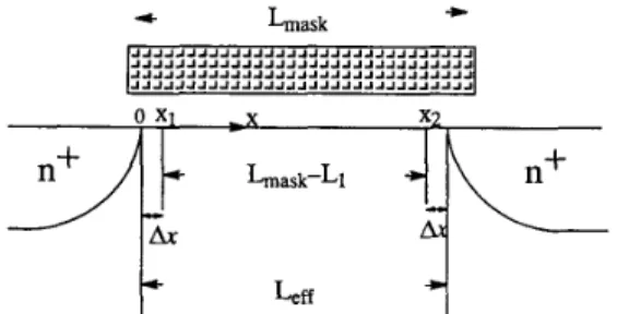
LI AND WU: NOVEL EXTRACTION TECHNIQUE FOR EFFECTIVE CHANNEL LENGTH OF MOSFET DEVICES ~ 857 x;!
I
F
4-
Fig. 1. A schematic device cross section showing the definition of
L , f f , & a s k , L1 and A x .
become larger for short-channel MOSFET’s. The saturation velocity method seems to be a better one, but the accuracy is dependent on the extraction equation for the saturation velocity.
In this paper, a novel method using the charge pumping technique to extract the effective channel length is intro- duced. The basic principle of the proposed method is to measure the charge pumping current of a set of MOSFET devices with varying mask lengths. This technique doesn’t have the problems of the resistance method and is applicable to conventional and LDD MOSFET’s with either surface or buried channel. In Section 11, the basic principle of the charge pumping technique for the determination of the effective channel length is presented. The extraction technique using a
set of conventional n-MOSFET devices is demonstrated as an example. It is shown that the extracted effective channel length is almost the same for different measuring conditions used. In addition, the proposed method is also applied to the case
of LDD n-MOSFET’s. Furthermore, the extracted
AL’s
are compared to those using the resistance method and a very good agreement is achieved only for the conventional MOSFET’s. In Section IV, the possible errors produced by the extraction process are discussed. A conclusion is made in the last section.11. BASIC PRINCIPLE
The charge pumping technique has been developed to measure the Si/SiOz interface-trap parameters in MOSFET devices [ 1 11-[25]. In general, the charge pumping phenomena can be explained by the Shockley-Read-Hall theory [15]. According to the Shockley-Read-Hall theory, the capture and emission rates of electrons and holes through the Si/SiOz interface traps can be written as
Rhc(Et, 2 ,
t )
= V t h c p n i exp(Ei - EFP)’%t(Et, 2,t ) ,
(1)Ree(Et, X!
t )
= V t h C n %exp(Et
- Ei)7Lit(Et!x!
t ) .
(4) For the steady state in a periodic waveform, the net electron density transferred in one repetition period (T,) from theconduction band of the semiconductor to the Si/SiOZ interface traps located at Et is equal to that transferred from Et to the valence band of the semiconductor. As shown in Fig. 1, the net charge density transferred through Et in one period at the position z along the Si/SiO2 interface can be expressed as
The charge pui,iping current density at z can be derived by integrating all the Si/SiOp interface-trap levels in bandgap and can be written as
Then, the total charge pumping current can be calculated by
where g(z) is a shape function with the value between 0 and
1. It is clear that only the Si/SiOz interface traps in the region where the silicon surface being cycled between accumulation and strong inversion will contribute to the charge pumping current. If the edges of this area are sharp, the “effective area” approach will be very accurate. This means that g(z)
is equal to 1 in the effective area and equal to 0 outside the area. If the interface-trap density is constant along the channel and the source/drain proximity effect [25] due to the potential perturbation near the source/drain junctions can be ignored, IC,, m a z ( z ) in (7) is a constant and is equal to IC,, l , I ( I r , then
(7) can be simplified as
where
L,,
is the effective length of the effective area. From(8) and Fig. 1, the
Le,
can be expressed asNote that the uniformity of the interface-trap density along the channel, the source/drain proximity effect, and the sharpness of the effective area edges will be discussed later.
The basic principle of the proposed method is to measure the charge pumping currents from a set of MOSFET devices with varying mask lengths. Plotting (8) versus
&ask,
the interceptL1
at the &ask axis can be derived.If the distance from metallurgical source/drain junctions to the nearby surface depletion edges under the gate is defined
as
Ax
and the source/drain islands are symmetrical, as shown in Fig. 1, the effective channel length can be expressed as858 IEEE TRANSACTIONS ON ELECTRON DEVICES. VOL. 42, NO. 5 , MAY 1995
-0.05 0.05 0.1 0.15 0.2
Lateral Surface Distance to Drain Junction(um) Fig. 2.
device simulator.
The method for determining Ax for a specified p , using a 2-D
PULSE GENERATOR I
T
Vd,
VsI
@
Current Meter““t
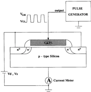
1
-Fig. 4. Setup used for the charge pumping measurement.
Fig. 3. Gate pulses used and the definition of the related parameters.
be expressed as
To obtain A x , the edges of the effective length must be determined. Note that the magnitude of A x is dependent on the applied source/drain bias during the charge pumping measurement. Due to the nonideal charge pumping current shape, the surface depletion edges of the effective length is defined as g ( x 1 ) = g(xp) = 0.5. From [24], when TL is kept constant and VGH strongly inverts the silicon surface, the half-maximum of I c P / f is only related to a specified surface hole concentration which is defined as the critical hole concentration ( p c ) . With the specified p,, the Ax can be obtained easily from a 2-D device simulator, as shown in Fig. 2.
To obtain p,, the
IC-/
f versus V& curve of a long-channel MOS device should be measured because the charge pumping current contributed by the source/drain proximity effect can be ignored. The applied gate waveform is shown in Fig. 3 ,in which VGH is kept constant to strongly invert the silicon surface; TH is a constant and is long enough to fill all the “effective interface traps” with electrons during VGH
.
The “effective interface traps” is defined to be all the interface traps that can contribute the charge pumping current. TL and SR1s.P are kept the same as those used to derive L1 and the period changes with VGL. It should be noted that the waveforms used should be careful to prevent the effect of the geometric current. From the I,,/ f versus VGL curves, the gate voltage related to the half-maximum of Ic,/f can be derived. Then, the critical hole concentration in the channel can be calculated using a numerical 2-D device simulator. Using the similar waveforms to measure L1, the edges of the effective area, named s1 and .r2 shown in Fig. I , can be defined as the positions where the surface hole concentration is p , at VGL. Since the hole concentrations near .r1 and .1‘2 vary rapidly, the“effective area” assumption is reasonable. The error introduced from this assumption will be discussed in Section IV.
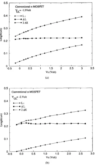
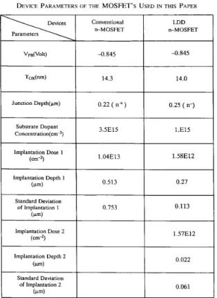
111. EXPERIMENTAL METHOD AND RESULTS The experimental transistors used to demonstrate the novel method in detail are n-channel MOSFET’s with different drawn channel lengths of 0.7, 0.8, 1.0, and 1.2 pm and the channel width of the devices is 100 pm. The related device parameters are listed in Table I. The setup used for the charge pumping measurement is illustrated in Fig. 4. Several S R and S F values of the gate pulses are used to extract L1 while VGL and TL are kept the same. With the same VGL and TL, the effective area is kept the same. As shown in Fig. 5, the extracted L1 using different
SR
andSF
are almost the same with a standard deviation of about 0.001 pm. This means that the extracted results are insensitive to the measuring gate waveforms and the error introduced from the measurement itself is small. Note that the VGL value used is -1.5 V for Fig. 5(a) and -2.0 V for Fig. 5(b). It should be noted thatLI AND WU: NOVEL EXTRACTION TECHNIQUE FOR EFFECTIVE CHANNEL LENGTH OF MOSFET DEVICES 859 300 200 v
z
100 n Conventional n-MOSFET T g T rloOOns.Vd=Vs=Z 4Volt t.Penod=bSDD ns-
Penod=Moo ns Penod=3200 ns-
Penod=ZMM ns 0.0 0.3 0.6 0.9 1.2 1.5 Lmask(um) (a) 300 200 hd
v2
100 n Conventional n-MOSFET vGL=-2.0Volr. [email protected] T c T ~lORlns.Vd=Vs=2.4VoIr-
Period48W ns-
Period& ns t* Period=3200 ns-
Period=ZMM ns 0.0 0.3 0.6 0.9 1.2 1.5 Lmask(um) (b)Fig. 5. The L1 extraction from the conventional nMOSFET's using several waveforms with TH = T L = 1000 nsec, I:\ = I;, = 2.4 V. (a)
I,:;,, = -1.5 V, l i ; H = 4.5 V. (b) Ti;[, = -2. V, I;-;[< = 4. V.
the applied source/drain biases are restricted to a range so
that the source/drain junction leakage current is much smaller than the charge pumping current. As the source/drain reverse bias increases, the junction depletion width at a fixed VGL increases and the effective area becomes smaller. Therefore, the deduced L1 increases with the source/drain bias, as shown in Fig. 6. Usually, the Si/SiOz interface-trap density is constant in the channel region and may vary near the source/drain junctions [23] due to the variations of dopant concentration near the source/drain junctions and the mechanical stresses at the polysilicon-gate edges. If the interface-trap density increases near the effective area edges, the deduced A L will be underestimated. Therefore, we should choose proper measurement conditions so that the effective area edges may locate in the channel region.
To suppress the current ratio induced by the source/drain proximity effect, the long-channel devices are suggested to be used to derive the I,,/f versus VGL curves. However, the device with the drawn channel length of 100 pm is the only-long channel device in our test pattern. For such a long
0.5 0.4
-
0.35
2 0.25
0.1 n Conventional n-MOSWT V GL =-I.SVolt "-0.5 0 0.5 1 1.5 2 2.5 3 3.5 vs (volt) (a) 0.5 0.4-
0.35
%
5 2 0.2 0.1 0 Conventional n-MOSFET v = -2.Volt GL-
L l -AL 1.0 0.5 1.0 1.5 2.0 2.5 3.0 vs (Volt) (b)Fig. 6 . The extracted L 1 . 2 1 . ~ . and A L versus different T - < / I n with (a)
I ~ ; L = -1.5 V. (b) I>~;r1 = -2 V.
channel device, the SR and S F of the gate pulses should keep small to prevent the geometric current, as shown in Fig. 7(a) ( S R = S F = 100 V/sec). Such low-frequency waveforms are not suitable for the charge pumping current measurement of the short-channel devices, because the measured current will be too small (near the resolution of the current meter) to derive L1 accurately. Therefore, the charge pumping current difference of two MOSFET's with different Lnlnsk are used to derive p,, as shown in Fig. 7(b). Using this method, we can derive the Ic,/f versus VGL curves at high frequencies without both the source/drain proximity components and the geometric component of charge pumping current. Using the device dopant profiles derived from the calibrated SUPREM
IV process simulator for a two-dimensional device simulator, the surface hole concentration related to the half-maximum of I,,/ f can be calculated. The derived p , is 1.65E15 cmP3. Note that the accuracy of the substrate doping profile had been verified by simulating the subthreshold current versus different back-gate biases.
The L1 and 2A.7: related to the source/drain bias with VGL =
860
Conventional n-MOSFET
IEEE TRANSACTIONS ON ELECTRON DEVICES, VOL. 42. NO. 5 . MAY 1995
LDD n-MOSFET
TABLE 1
DEVICE PARAMETERS OF THE MOSFET’s USED I N T H I S PAPER
Vm(V0lt) Tox(nm) 4 . 8 4 5 4 . 8 4 5 14.3 14.0 Junction Depth(p” 0.22 ( n’) 0.25 ( n-) 3.5E15 1.E15
I
Substrate Dopant Concentration(cm-3)I
1.58E12 Implantation Dose 11
(cm-z)I
1.04E13 0.27 Standard Deviation of Implantation 1 0.753 0.113 I I II
Implantation Dose 2 (Cm-2)I
I
1.57E12 Implantation Depth 2I
(w)I
0.022 Standard Deviation of Implantation 2I
0.061derived from (1 1) are 0.220 and 0.219 pm, respectively. Fig. 8
shows the deduced AL using the resistance method. Compared to the extracted A L using the charge pumping method, the resistance method overestimates the AL value for low gate voltage ( V ~ S - V, - 0 . 5 V ~ s
<
1.OV) due to the invalidity of the linear-region current equation used and underestimates theAL
value for high gate voltage (VGS - V+ 0.5 V ~ S>
1.0 Volt) due to the inclusion of n+ tail. Compared to the resistance method, the charge pumping method has a smaller extraction deviation and is self-consistent at any measurement condition.
One of the major advantages of the charge pumping method is that it is suitable to all kinds of the MOSFET devices with substrate contacts. A set of LDD nMOSFET’s are used for the
A L
extraction, the drawn channel lengths are 0.6, 0.7, 0.8, and 0.9 pm, respectively. The AL extraction process is the same as that applied to the conventional nMOSFET’s. The device parameters are also listed in Table I. For the LDD devices, the measurement error for L1 is still small and the derived AL is 0.26 pm, as shown in Fig. 9 and Fig. 10(a). The reliable AL values are derived from the higher source/drain voltages, because the edges of the effective area may locate in the channel region. The interface-trap density near the source and drain junctions could be higher than that in the channel, and this will introduce the underestimation of A L if the effective area edges are located near the source/drain region.0.08 0.06 ?-.
8
4, 0.04 F”
0.02 Conventional n-MOSFET Lmask= 100 um 0 -2.0 -1 .o 0.0 VGdVolr) (a) 0.3 Conventional n-MOSFET Lmask 1.2um- 1.Oum0 -2.0
:
-1.0.
VGIlVOlt) 0.0,
(b)
Fig. 7. The Icp/f-\kJ, curve derived from (a) A single n-MOSFET with
L 7 T t c , s k = 100 p m . (b) The difference of two n-MOSFET devices with different L n , c l s k . 0.4 0.3
-
5
0.2 =i 0.1 0.0 c 1- 1 Conventional n-MOSFET 0.5 1.0 1.5 2.0 2.5 3.0 3.5 V g s - b -O.SVds(Volt) D Fig. 8.the resistance method.
The extracted AL from the conventional n-MOSFET devices using
method are shown in Fig. 10(b). It is clearly seen that the For comparisons, the AL values derived from the resistance extracted AL’s using the resistance method are strongly gate-
LI AND WU: NOVEL EXTRACTION TECHNIQUE FOR EFFECTIVE CHANNEL LENGTH OF MOSFET DEVICES 0.5 0.4 0.3
E
zi
0.2 0.1 ~ 86 1 - LDD n-MOSFET v =-1JVolt --
GL Ll -:
-:
;
- 400 3002
4 2003
100 0.4 Es
0.3 0.2 LDD n-MOSFET k L = - 1 SVoll. [email protected] T r T ~lOoons.Vd=Vs=l.Wolt t.Mod4800ns-
Pcriod=dMo ns +--+ Period=3Mo ns F--T Period=2600 ns -:--.
- 0 0 0.3 0.6 0.9 1.2 Lmask(um) Fig. 9.derive L1 from the LDD nMOSFET.
Charge pumping current versus L m n s k for several frequencies to
bias dependent. Similarly, the resistance method overestimates the
A L
value for low gate voltage and underestimates theAL
value for high gate voltage. Therefore, the charge pumping method becomes important to extract the metallurgical channel length, especially in the case of LDD devices.
IV. DISCUSSION
The accuracy of this new technique and the validity of several assumptions used are discussed in this section. Con-
ventional n-channel MOSFET’s are used as an example. The errors introduced by the deviation of p,, the waveform rise/fall slopes, the effective area approach, and the source/drain prox- imity effect are discussed.
A. p , Deviation and Waveform RiseIFall Slopes
The p , is a key parameter of this extraction technique. If the derived
A L
is sensitive to p,, a serious error can be generated due to a bad estimation of p,. For example, if 50% error for the substrate dopant profiles is given by SUPREM IV, then about 100% error of p , is produced. To discuss the sensitivityof AL related to p,, we calculate
2Ax
related to both p , =1.65E15 and
3.3E15
~ m - ~ , as shown in Fig. 1 1 . The2Ax
(orAL)
deviations due to 100 % p c error are still acceptable and are less than 0.007 pm. Besides, according to the recent study[24], the p , is only sensitive to TL. Therefore, the p , variation related to the four S R / S F values used in Fig. 5(a) and (b) are small and the induced A L difference can be ignored. B. The Effective Area
The effective area approach is used for the simplicity of the A L extraction shown in Section 11. If Icp, m a z ( x ) is constant along the channel, then
IC,(.)
is only related to the surface hole concentration of x at VGL [24]. The total charge pumping current can be expressed as-0.1
I
-0.5 0.0 0.5 1.0 1.5 2.0 2.5 3.0 3.5 vs (Volt) (a)1::
j
LDD n-MOSFET vgs-v, o.5vds(volt) (b) Fig. 10.(b) A L extracted from the resistance method.
LDD nMOSFET devices. (a) L1, 2Ax and AL versus Vs/V,.
0.3 q
I
Conventional n-MOSFETkL=
-1.5VOlt C.Pc=1.65E15 0.251
I
+ --
Pc=3.3E15 0.21
0 ’ -0.5 0 0.5 1 1.5 2 2.5 3 vs (Volt) 5 Fig. 1 1 .1.65E15 and 3.3E15
2Ax versus V ~ / V D with critical hole concentration of p c =
where g ( p , ) is the weighted factor related to the surface hole concentration. The g(VGL) can be derived easily from
the
IEEE TRANSACTIONS ON ELECTRON DEVICES. VOL. 42, NO. 5, MAY 1995 0.0 862 1 .o
-
$ 0.8s
2 0.6 C 3 f5
0.4 0.2-
K‘j
* z r e a l g ( x )effective area approach
IC,/
f
versus VGL curves in Fig. 7(b). The I c p / f in Fig. 7(b) can be expressed as1 c p I . f = (IC,, m a z / f ) a L m a s k . Y ( ~ G L ( P ~ ) ) (13) where ALnLask is the drawn channel-length difference of two devices. Using a numerical 2-D device simulator to calculate the relation between V ~ L and ps, the g ( p , ) can be derived.
On the other hand, the weighted factor of the effective area approach, g e ( p s ) , can be expressed as
&(Pa) = 1. if P E
2
Pc.q,(ps) = 0. if P ,
<
p C .The .9(p,) and g e ( p s ) near the junctions are plotted in Fig. 12. The error of the effective area approach can be derived as
As shown in Fig. 12, the L,,.,,, is less than 0.001 pm. C. Potential Perturbation Near the Source/Drain Junctions
I c p , m o z ( ~ ) in (7) is assumed to be a constant to derive
(1 1). However, Icp, n L a z ( - l . ) is not exactly constant along the
channel, even the interface-trap density is constant. At the proximity of source and drain junctions, the nonsteady-state emission times for electrons and holes are different. We can estimate the charge pumping current density using the equations derived by Groeseneken [ 141 :
I c p , m a z ( l ) = 2 y Z . f kBT[l71 ( u t h 7 ) ~ 4 % & )
f0.5171 ( t e n , . e(.)
t,,,,,
h ( J ) ) ] . (15)The induced error can be approximated by
Lcrrm = /,:(IC,, m a x ~ - IC,, m a z ( ~ ) ) / 1 c p , m a z ~ d~ (16) where 3’1 and x2 are the edges of the effective area and IC,, m a z ( ) is the charge pumping current density near the middle of the channel. The L,,,,, is about 0.001 pm at VGL =-1.5 V and VD/Vs = 3 V.
From the above discussions, we conclude that 0.01 pm accuracy of A L extraction is feasible using the proposed charge pumping method.
V. CONCLUSION
The charge pumping technique is shown to be a simple and accurate method to extract the effective channel length of MOSFET’s. Similar to the capacitance method, no I-V models are needed for the AL extraction. It is shown that the proposed novel method is a direct measurement of L , f f with much higher resolution. The derived results are clear, reliable, and independent of the measurement biases. With the knowledge of the device dopant profiles, 0.01 pm accuracy can be achieved easily. In addition, this method is applicable to either n- or p- channel, conventional or LDD, surface or buried channel MOSFET’s.
ACKNOWLEDGMENT
Special thanks are given to Submicron Technology Divi- sion, Electronics Research and Service Organization, Industrial Technology Research Institute, Taiwan, Republic of China, for providing the test devices, especially to M. C. Chang and Dr.
P. S. Lin.
REFERENCES
[ I ] K. Terada and H. Muta, “A new method to determine effective MOSFET channel length,” J. Appl. Phys., vol. 18, pp. 953, 1979.
[2] J. G. J. Chern, P. Chang, R. F. Motta, and N. Godinho, “A new method to determine MOSFET channel length,” IEEE Elect. Device Lett., vol.
1, pp. 170, 1980.
[3] K. L. Peng and M. A. Afromowitz, “An improved method to determine MOSFET channel length,” IEEE Elect. Device Lett., vol. 3, pp. 360,
1982.
[4] J . Y. C. Sun, M. R. Wordeman, and S. E. Laux, “On the accuracy of channel length characterization of LDD MOSFET’s,” IEEE Truns.
Electron Devices, vol. 33, pp. 1556, 1986.
[51 D. J. Mountain, “Application of electrical effective channel length and external resistance measurement techniques to submicrometer CMOS Process,” IEEE Trans. Electron Devices., vol. 36, pp. 2499, 1989. 161 G. J. Hu, C. Chang, and Y. T. Chia, “Gate-voltage-dependent effective
channel length and series resistance of LDD MOSFET’s,” IEEE Trcms.
Electron Devices, vol. 34, pp. 2469, 1987.
171 D. Wilson, A. J. Walton, J. M. Robertson, and R. J. Holwill, ‘‘1~5 extraction using parasitic bipolar transistors,” in Proc. IEEE 1988 Int. Conf Microelectronic Test Structures, vol. I , pp. 85, 1988.
[8] J. Ida, A. Kita, and F. Ichikawa, “A new extraction method for effective channel length on lightly doped drain MOSFET’s,” in Proc. IEEE 1990
Int. Con5 Microelectronic Test Structures, vol. 3 , pp. 117, 1990.
[9] S . Nakanishi, M. Hoijer, Y . Saitoh, Y. Katoh, Y. Kojima, and M. Kamiya, “Effective channel length determination using punchthrough voltage,” in Proc. IEEE I992 Int. ConJ Microelectronic Test Structures, vol. 5 , pp. 73, 1992.
[IO] B. J . Sheu and P. K. KO, “A capacitance method to determine channel lengths for conventional and LDD MOSFET’s,” IEEE Electron Device
Lett., vol. 5 , pp. 491, 1984.
[ I I ] J . S. Burgler and P. G. Jespers, “Charge pumping in MOS devices,”
IEEE Trans. Electron Devices. vol. 16. pp. 297, 1969.
[12] A. B. Elliot, “The use of charge pumping currents to measure surface state densities in MOS transistors,” Solid Stcrte Electron., vol. 19, pp. 241, 1976.
[I31 T. J. Russell, C. L. Wilson, and M . Gaitan, “Determination of the spacial variation of interface trapped charge using short-channel MOSFET’s,”
IEEE Trans. Electron Devices. vol. 30, pp. 1662, 1983.
[I41 G. Groeseneken, H. Maes, N. Beltran, and R. DeKeersmaecker, “A reliable approach to charge-pumping measurements in MOS transistors,”
IEEE Trun. Electron Devices. vol 31, pp. 42, 1984.
[IS] U . Cilingiroglu, “A general model for interface-trap charge-pumping effects in MOS devices,” Solid-Stcrte Electron.. vol. 28, pp. 1127, 1985.
LI AND WU: NOVEL EXTRACTION TECHNIQUE FOR EFFECTIVE CHANNEL LENGTH OF MOSFET DEVICES 863
1161 W. L. Tseng, “A new charge pumping method of measuring Si/SiOa interface states,” J. Appl. Phys., vol. 62, pp. 591, 1987.
[I71 F. Hofmann and W. H. Krantschneider, “A simple technique for determining the interface trap distribution of submicron MOS transistors by the charge pumping method,” J. Appl. Phys., vol. 65, pp. 1358, 1989. [18] J. E. Chung and R. S. Muller, “The development and application of a Si/SiOz interface-trap measurement system based on the staircase charge-pumping technique,” Solid-State Electron., vol. 32, pp. 867, 1989.
[I91 N. S. Saks and M. G. Ancona, “Determination of interface trap capture cross-sections using three-level charge pumping,” IEEE Electron Device Lett., vol. 11, pp. 339, 1990.
[20] G. Van den Bosch, G . V. Groeseneken, P. Heremans, and H. E.
Maes, “Spectroscopic charge pumping: A new procedure for measuring interface trap distributions on MOS transistors,” IEEE Trans. Electron Devices, vol. 38, pp. 1820, 1991.
[21] G. Ghibaudo and N. S. Saks, “A time domain analysis of the charge pumping current,” J. Appl. Phys., vol. 64, pp. 4751, 1988.
[22] W. Chen and T. P. Ma, “A new technique for measuring lateral dis- tribution of oxide charge and interface traps near MOSFET junctions,” IEEE Electron Device Lett., vol. 12, pp. 393, 1991.
[23] M. G. Ancona, N. S. Saks, and D. McCarthy, “Lateral distribution of hot-carrier-induced interface traps in MOSFET’s,” IEEE Trans. Electron Devices, vol. 35, pp. 2221, 1988.
[24] H. H. Li and C. Y. Wu, “A new analytic charge pumping current model,” submitted to IEEE Trans. Electron Devices for publication.
[25] M. Gaitan, E. W. Enlow, and T. J. Russell, “Accuracy of the charge pumping technique for small geometry MOSFETs,” IEEE Trans. Nucl. Sci., vol. 36, pp. 1990, 1989.
Hsin-Hsien Li (S’87) was born in Taiwan, Republic of China, in 1964. He received the B.S. degree in electrical engineering from the National Cheng Kung University, Taiwan, in 1986, and the M.S. degree from the Institute of Electronics, National, Chiao-Tung University, Hsinchu, Taiwan, in 1988. He is currently working toward the Ph.D. degree and engages in deep-submicrometer MOS device physics and reliability issues.
Mr. Li is a member of Phi Tau Phi.
Ching-Yuan Wu (M’72) was born in Taiwan, Re- public of China, on March 18, 1946 He receive the
B S degree in electrical engineenng from the Na-
tional Taiwan University, Taiwan, in 1968, and the M.S. and P h D degrees from the State University of New York at Stony Brook in 1970 and 1972, respectively
During the 1972-1973 academ~c year, he was appointed as a Lecturer in the Department of Elec- trical Sciences at SUNY-Stony Brook During the 1973-1975 academic years, he was a Visiting As- sociate Professor at the National Chiao-Tung University (NCTU), Taiwan. In 1976, he became Full Professor in the Department of Electronics and the Institute of Electronics at NCTU While there he was the Director of the Engineering Laboratories and Senuconductor Research Center from 1974 to 1980, the Director of the Institute of Electronics from 1978 to 1984, and ,he Dean of the College of Engineering from 1984 to 1990 He was a principal investigator of the National Electronics Mass Plan-Semiconductor Devices and Integrated-Circuit Technologies from 1976 to 1979, and had been a Coordinator of the National Microelectronics Researches and High-Level man- Power Education Committee, National Research Council, Republic of China from 1982 to 1988 He has been the Research Consultant of the Electronics Research and Service Organization (ERSO), ITRI, a member of the Acadenuc Review Committee in the Ministry of Education, and the chairman of the Technical Review Committee on Information and Microelectronics Technolo- gies at the Ministry of Economic Affairs His research activities have been in semiconductor device physics and modeling, integrated-circuit designs, and technologies His current research areas focus on the developments of efficient 2D and 3D simulators for deep-submicrometer semiconductor devices, design rules and optirmzation techniques for deep-submicrometer CMOS devices He has published over 180 papers in the sermconductor field and has served as a reviewer for international journals such as IEEE ELECTRON DEVICE LETTERS, IEEE TRANSACTIONS ON ELECTRON DEVICES and Solid State Electronics
Dr Wu is a member of the Honorary Editorial Advisory Board of Solrd-
State Electronics, and is a board member of the Chinese Engineering Society. he received the Academic Research Award in Engineering from the Ministry of Education (MOE), in 1979 and the Outstanding Scholar Award from the Chinese Educational and Cultural Foundation in 1985 He received the outstanding research Professor fellowship from the Ministry of Education and the National Science Council (NSC), Republic of China from 1982 to 1995 He received the D~stinguished Engineering Professor Medal Award from the Chinese Engineering Society in 1992