Ownership and Copyright
2002 Springer-Verlag London Limited
A Practical Implementation of Parallel Dynamic Load Balancing for
Adaptive Computing in VLSI Device Simulation
Y. Li
1,2,*, S. M. Sze
1,3and T.-S. Chao
1,41National Nano Device Laboratories, Hsinchu, Taiwan;2Microelectronics and Information Systems Research Center,3Department of Electronics Engineering,4Department of Electrophysics, National Chiao Tung University, Hsinchu, Taiwan
Abstract. We present a new parallel semiconductor device simulation using the dynamic load balancing approach. This semiconductor device simulation based on the adaptive finite volume method with a posteriori error estimation has been developed and successfully implemented on a 16-PC Linux cluster with a message passing interface library. A construc-tive monotone iteraconstruc-tive technique is also applied for solution of the system of nonlinear algebraic equations. Two different parallel versions of the algorithm to perform a complete device simulation are proposed. The first is a dynamic paral-lel domain decomposition approach, and the second is a parallel current-voltage characteristic points simulation. This implementation shows that a well-designed load balancing simulation can significantly reduce the execution time up to an order of magnitude. Compared with the measured data, numerical results on various submicron VLSI devices are presented, to show the accuracy and efficiency of the method.
Keywords. DTMOS; Dynamic domain decomposition;
Linux cluster; Load balancing; MOSFET; Parallel I– V points calculation; VLSI device simulation
1. Introduction
Numerical modeling and simulation of Very Large Scale Integration (VLSI) devices has been proven to be an indispensable tool for the analysis and optimal design of various semiconductor devices [1]. Computational methods for macroscopic semi-conductor device models, such as the Drift-Diffusion (DD) and Hydrodynamic (HD) models, play a cru-cial role in the development of semiconductor device simulators. As the dimensions of devices continue to shrink [1–5], the development of sophisticated and efficient multi-dimensional semiconductor
Correspondence and offprint requests to: Dr Yiming Li, P.O. Box 25–178 Hsinchu City, Hsinchu 300, Taiwan. E-mail: ymli얀cc.nctu.edu.tw
device Technology Computer Aided Design (TCAD) software provides engineers with significant leverage in conducting research into new integrated circuit technologies. Computer-aided semiconductor device simulations [6–28] provide the capability for a software-driven approach to new device design, because of the ability to test new chip designs before fabrication. It may result in considerable speedup in the development cycle, and hence a significant reduction in the cost. However, the increasing complexity of device simulators has in the past led to many difficulties in extending the physical and numerical capabilities. This growing demand urges more advanced software programming techniques; for example, parallel and adaptive com-putation provide an alternative for VLSI device simulation [29–39].
Parallel computations have received considerable attention in TCAD applications [20–24]. The avail-ability of powerful CPUs and high-speed networks makes a cluster of computers a very powerful tool for cost-effective, high performance computing in scientific and engineering applications. A cluster of PCs connected by a high-speed network becomes a viable platform for running computation-intensive parallel applications. In addition, adaptive compu-tation is currently one of the main concepts in practical and large-scale computations [25–39]. Considerable effort has recently been directed towards the development of numerical techniques for semiconductor device equations. The paralleliz-ation of numerical simulparalleliz-ations with an adaptive mesh is a very complex task. By focusing the computing resources on those regions with a high relative error, the use of unstructured mesh and Monotone Iterative (MI) technique [7,20,21,40–42] has the great potential of producing large compu-tational and storage savings, but it also has the price of increasing the sophistication of codes and
algorithms. Because of the irregular load require-ments of parallel adaptive computation, a mesh must also be repartitioned for processors during runtime. Under a cluster parallel computing environment [43– 45], adaptation of the mesh produces imbalances in the jobs assigned to processors.
In this paper, we present an approach to a parallel dynamic partition for adaptive computing in sem-iconductor device simulation. Based on the adaptive unstructured mesh generation, a posteriori error esti-mation, Finite Volume (FV) discretization [46–49], and the Gummel’s decoupling algorithm, 2D sem-iconductor device models are decoupled and discret-ized, and hence a system of nonlinear algebraic equations is obtained. We solve the nonlinear system by means of the MI method, instead of the conven-tional Newton’s Iteration (NI) method. The MI method is a constructive technique for the numerical solution of Partial Differential Equations (PDEs) [41,42]. Compared with the NI method, the applied MI method for VLSI device simulation has some merits: (1) global convergence, (2) easier implemen-tation, and (3) ready for parallelization [7,20,21,40]. These properties guarantee that the proposed parallel algorithms – the dynamic parallel domain decom-position approach and the parallel current-voltage (I–V) characteristic points simulation – work well through the study.
For most practical submicron device structures, the electrostatic potential, carrier concentrations and temperature exhibit extreme layers, particularly in the neighborhood of p-n junctions. This implies a local adaptive mesh refinement strategy for un-structured grids [25–28]. Our study is based on this physical phenomenon, and a posteriori error estimation. However, the adaptive computation duces load imbalances among processors. We pro-pose a physical-based parallel adaptation and load balancing algorithm for repartitioning and rebalanc-ing of the workload. The algorithm supports a dynamical changing mesh environment, where the nodes and corresponding unknowns migrate instan-taneously between the numbers of processor to balance the workload in each refinement level. Com-putational results for the PN diode, N-channel Metal-Oxide-Semiconductor Field-Effect Transistor (N-MOSFET), and Dynamic Threshold voltage MOS-FET (DTMOS) are presented to show the accuracy of the model and efficiency of the solution method, including parallel speedup achieved with respect to the number of CPUs on a Linux cluster with a Message Passing Interface (MPI) library [43,45].
The paper is organized as follows. Sections 2 and 3 describe the semiconductor device models and
adaptive computing method, respectively. Section 4 states the parallel domain decomposition with dynamic load balancing and parallel I–V points simulation. Section 5 includes the results and dis-cussion. Section 6 draws conclusions and suggests future work.
2. Semiconductor Device Models
Recently, HD models for submicron semiconductor device modeling have received considerable atten-tion in the study of hot carrier and non-local effects [6,8–10,12,14,15,17,24]. One of the HD models con-sists of at least five coupled nonlinear PDEs for an electron and a hole. A set of the stationary HD equations in semiconductor device simulation is as follows [9,10,17]: ⌬ = q ⑀s (n− p + D) (1) 1 qⵜ·Jn= R(n, p) (2) 1 qⵜ·Jp= − R(n, p) (3) ⵜ·Sn= Jn·E− n
冉
n− 0 n(Tn)冊
(4) ⵜ·Sp= Jp·E− p冉
p− 0 p(Tp)冊
(5) where is the electrostatic potential, n and p are electron and hole concentrations, and Tn and Tp arethe electron and hole temperatures. The electric field
E is defined by E = −ⵜ, q is the elementary
charge,⑀sis the dielectric constant of semiconductor,
0 is the average carrier energy in the thermal equilibrium, and the net doping concentration is
D(x, y)= N+
D(x, y)− N−A(x, y) [2,14]. The net
recom-bination rate R includes the Shockley–Read–Hall recombination process, and the energy relaxation time approximations for the electron and hole are n and p, respectively [2–4,6,8–10,14,15,17– 19,24]. The average carrier energy is sum of the thermal and drift energy that is given by
n= 3 2kBTn + 1 2m ⴱ n2n (6) p= 3 2kBTp + 1 2m ⴱ p2p (7)
for the electrons and holes, respectively. The
mⴱnand mⴱp are the electron and hole effective
mean velocities. The expressions for the carrier’s currents and energy flux densities Jn, Jp, Sn, and Sp
are given by Jn= −qnnⵜ + qDnⵜn + nkBnⵜTn (8) Jp= −qppⵜ + qDpⵜp + pkBpⵜTp (9) Sn = Jn −q n + Jp −qkBTn + Qn (10) Sp = Jp +qp+ Jp +qkBTp+ Qp (11)
where the carrier mobility n and p depend upon
the doping profile, carrier concentration, electric field and energy. The diffusion coefficients Dn and Dp
are assumed to satisfy the Einstein relation. The heat flows Qn and Qp are modeled by a scalar
thermal conductivity times the negative gradient of the carrier temperature [2–4,6,8–10,14,15,17–19,24]. The unknowns to be solved in Eqs (1)–(5) are ,
n, p, Tn and Tp, respectively.
Over the past decade, the most widely used and successful device modeling has been the DD equa-tions. If the local thermal equilibrium assumption is valid for semiconductor devices, this model can still be used for device design and research [1–4,7,9,11– 14,16,18–29]. The DD model consists of Eqs (1)– (3) as stated above, and the physical quantities have the same meaning as with the HD model. However, the expressions of Jn and Jp for the DD model are
reduced to
Jn = −qnnⵜ + qDnⵜn (12)
Jp = −qppⵜ + qDpⵜp (13)
where the unknowns to be solved in Eqs (1)–(3) are , n and p, respectively.
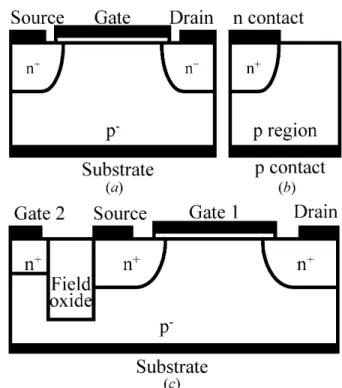
Figure 1 shows cross-section views of the N-MOSFET, PN diode and DTMOS devices studied in the (x, y) plane. Both these models are subject to mixed type boundary conditions on the boundary of the device domain. The boundary conditions of electrons for the HD model (similar to the DD model) are stated as follows [2–4,9,14,17]. For an N-MOSFET, shown in Fig. 1(a), on the source, gate, drain and substrate ohmic contacts we assume the Dirichlet boundary conditions for , n and Tn
= Vapp+ kBTL q D 兩D兩ln
冢
兩D兩 2ni +冪
冉
D 2ni冊
2 + 1冣
(14) n=D 2 +冪
冉
D 2冊
2 + n2 i (15)Fig. 1. A schematic diagram for various devices: (a) N-MOSFET,
(b) P-N diode, (c) DTMOS.
Tn= TL (16)
where the TL is the lattice temperature, Vapp
rep-resents the applied voltage at the ohmic contacts, and ni is the intrinsic carrier concentration. At the
interface between the silicon substrate and gate oxide, by assuming that the charge in the oxide is negligible and the electric filed in the oxide is uniform, Gauss’ Law leads to the following Robin boundary condition for :
⑀s ⭸ ⭸n→ − ⑀ ox VG− tox = Q (17)
where Q is the interface charge density, VGindicates
the applied gate voltage, tox is the gate oxide
thick-ness, n→ is the outward normal vector, and ⑀ox is the
dielectric constant of oxide. Furthermore, we assume that the electron current flow and electron energy flux perpendicular to the interface equals zero:
Jn· n → = 0 (18) Sn·n → = 0 (19)
To guarantee that the simulated VLSI devices are self-contained, we apply the homogeneous Neumann boundary conditions on the left and right artificial boundaries:
⭸ ⭸n→ = 0, ⭸n ⭸n→= 0, and ⭸Tn ⭸n→ = 0 (20) We have similar boundary conditions for holes. To study the device transport behavior, including I–V curves, various numerical methods (e.g. Finite Difference (FD), FV (or so-called finite box), and Finite Element (FE) methods), together with NI methods have been developed [4,6,8–19,22–28] for the approximated solutions of the HD and DD mod-els. Different from the NI method, we apply the MI method to solve the corresponding nonlinear system.
3. Methods of Adaptive Computation
The adaptive computing procedure for semiconduc-tor device simulation includes: the Gummel’s deco-upled algorithm [7,9,11,13,14,18,19], FVM [46–49], MI method [7,20,21,40–42], error estimation tech-nique [20,21,25–39], and unstructured 1-irregular [38,39] mesh refinement method. The adaptive mechanism is based on estimation of the solution gradient and variation of the lateral current density, and a posteriori error estimation is applied to pro-vide local error indicators for incorporation into the mesh refinement strategy. The local error indicators guide the adaptive refinement process.
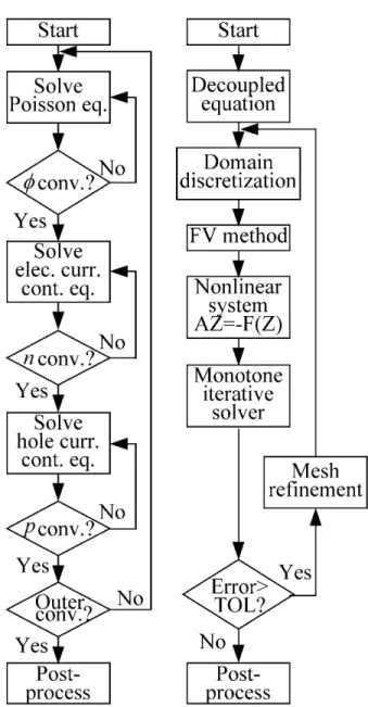
The transport behavior of submicron devices is governed with coupled PDEs, and is solved sequen-tially with Gummel’s decoupled [18,19] method. As shown on the left of Fig. 2, in the DD model the Poisson equation is solved for (g+1) given the pre-vious states n(g) and p(g). The electron current conti-nuity equation is solved for n(g+1) given (g) and
p(g). The hole current continuity equation is solved for p(g+1) given (g) and n(g). A similar procedure can be applied to decouple the PDEs of the HD model. Each decoupled PDE is solved with the adaptive computing algorithm.
The right flowchart in Fig. 2 shows the adaptive computation procedure for VLSI device simulation. For a given decoupled device PDE, we partition the solution domain into a set of disjoint FVs and approximate the PDE with the FVM. After FV discretization, we apply the MI method to solve the system of nonlinear algebraic equations directly. Once an approximated solution is computed, we perform a posteriori error analysis to assess its quality, and the error analysis produces error indi-cators and an error estimator. If the estimator is less than a specified error tolerance (TOL), the adaptive process will be terminated and the approximated solution can be output for post-process and analysis.
Fig. 2. Flowcharts for the Gummel’s decoupled (left) and
adaptive computing (right) methods.
Otherwise, we employ a scheme to refine current elements depending on the magnitude of the error indicator. A finer partition of the domain is thus created, and a new solution procedure is repeated iteratively. We summarize the adaptive computation procedure below.
쐌 Step 1. VLSI Device Model Formulation. The mathematical model for a set of semiconductor device equations, such as the HD and DD model, is formulated and decoupled with Gummel’s decoupling algorithm. Each decoupled PDE is solved with an adaptive computing algorithm sequentially.
Fig. 3. (a) 1-irregular FE (solid line) and FV (dot line) mesh.
(b) Control volumes for the FV mesh.
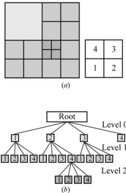
adaptive computation begins with a simple initial mesh and automatically generates an unstructured mesh by the refinement processes. Figure 3(a) shows the applied quadrangular FE and FV, where the control volumes are associated with the elements. The solid line is the FE mesh and the dotted line indicates the FV mesh. As shown in Fig. 3(b), based on our experience, we list 13 possible types of control volume for this unstruc-tured mesh, where the dots are regular points and cross-dots indicate irregular points. The FE and FV mesh refinement algorithm can be found in further detail elsewhere [26–39,46–49]. Figure
4(a) is a refined 1-irregular mesh and Fig. 4(b) shows there are 4 levelF0 cells, 12 levelF1 cells and 4 levelF2 cells. These cells are the children of the initial mesh; all the nodes built a list of tree and are stored in a dynamic data structure. 쐌 Step 3. FV Approximation and Exponential
Fit-ting. We discretize the decoupled device PDEs
with the FVM, and use the exponential fitting technique (the so-called Scharfetter–Gummel [18,19] scheme for the DD model and the Scharfetter–Gummel–Tang [15] scheme for the HD model) to locate sharp variations in the carrier concentration and energy. The fitting schemes are often used for the FV approximated current continuity and energy flux equations [6,8– 10,12,14,15,17,24] and have their merits.
쐌 Step 4. Solution of Nonlinear System. The conven-tional Gummel’s decoupling scheme for solving the DD model consists of three inner NI loops (five for the HD model) for each unknown func-tion, and an overall outer loop for all unknowns. Based on the nonlinear property of each PDE, we replace the NI method and solve the system of nonlinear algebraic equations with the MI method. We derived the MI formula for device simulation earlier [7,20,21,40]
Fig. 4. (a) Root and refined rectangular cells. (b) Data structure
(D +I)Z(m+1)= (L + U)(m)− F(Z(m)) +Z(m) (21) where Z is the unknown vector, F is the nonlinear vector form, and D, L, U and I are the diagonal, lower triangular, upper triangular and identity matr-ices, respectively. The MI parameter is determined node-by-node [7] depending on the device structure, doping concentration, bias condition and the nonlin-ear property of each decoupled PDE. We note in general that the NI method requires a sufficiently accurate initial guess to begin with the iterations, and forms a Jacobian matrix [14]. In contrast to the NI model, the MI method does not involve a Jacob-ian matrix, and the solution formula, Eq. (21), is of the Jacobi type and is ready for parallelization. 쐌 Step 5. A Posteriori Error Estimation. When the
approximated solution is computed, we perform
a posteriori error estimation for all elements [25–
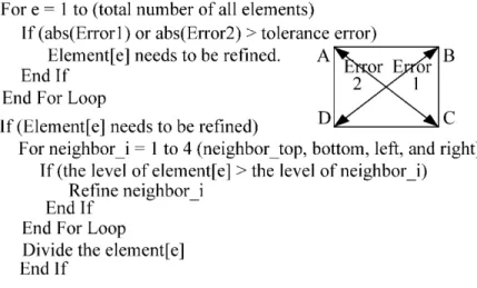
39]. As mentioned above, the computed solution exhibits large gradients within junctions and the channel surface. With this observation, the vari-ations of potential, electron concentration and electron current density are computed element-by-element to be a set of error indicators for the FV approximation. Figure 5 shows the pseudo-code for the error estimation and mesh refinement. We verify the global error estimators of the approximated solution. If it converges, we go to step 7; otherwise, we carry out step 6 for adaptive mesh refinement.
쐌 Step 6. Mesh Refinement. The 1-irregular mesh refinement scheme is applied to refine the mesh. Back to step 3 for the next computation.
쐌 Step 7. Post-process. The computed solutions are used for the next process or for calculating physical measurable quantities, such as the I–V curves [2–4].
Fig. 5. Pseudo-code for the error estimation and mesh refinement.
4. Parallel Algorithms and Load
Balancing
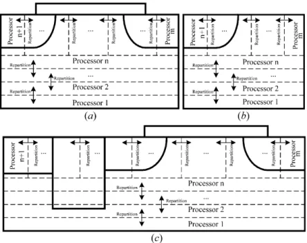
Two different parallel algorithms to perform a com-plete device characteristics simulation are presented here. One uses dynamic load balancing in a parallel domain decomposition approach; the other is a novel parallel I–V points simulation. The adaptive FV computation produces a number of nodes for a refined mesh that is much larger than the number of nodes in the initial mesh, and leads to a load imbalance. For parallel simulation a serial static graph partition algorithm has been designed to partition and distribute the initial mesh, but it is not so feasible to rebalance the workload of refined mesh [22–24]. We present a dynamic parallel domain decomposition algorithm, and describe the second parallel algorithm, the parallel I–V points calculation method for VLSI device simulation.
As shown in Fig. 6, based on different device structures and the bias condition, the simulation domain is dynamically partitioned into some disjoint sub-domains. When a refined tree structure is created, the number of processors for the next com-putation will first be dynamically assigned and allo-cated following the total number of nodes. We apply the geometric dynamic graph partitioning method in the x- or/and y-direction to partition the total number of nodes and assign those partitioned nodes to each processor. For the HD model simulation, each partition sub-domain contains five nonlinear systems (three nonlinear systems for the DD model) to be
solved, where the systems have arisen from
Gummel’s decoupled and adaptive FV approximated device PDEs. Once previous results are given, the boundaries for partitioned sub-domains are totally
Fig. 6. An illustration of the dynamic partition for various devices: (a) N-MOSFET, (b) P-N diode, (c) DTMOS.
separated, and we solve nonlinear systems with Eq. (21) independently. When newer MI solutions of nonlinear systems are computed, we perform the boundary data exchange for the next Gummel’s iteration loop. Figure 7(a) shows the pseudo-code for the parallel domain decomposition. The compu-tational procedure for the parallel domain decompo-sition consists of:
(A1) Initialize MPI and configurations; (A2) Establish 1-irregular mesh tree structure;
(A3) Count the number of nodes and apply a
dynamic partition algorithm to determine how many processors are required in this simul-ation, where all nodes are identified and num-bered;
(A4) Solve all assigned jobs with Eq. (21) and communicate data with the MPI protocol; (A5) Perform the error test for all elements and
run the refinement for the corresponding elements;
(A6) Repeats steps (A3)–(A5) until the error of all elements is less than a specified error bound; and
(A7) Host processor collects all computed results and stops the MPI.
As shown in Fig. 7(b), the dynamic partition algorithm for load balancing in step (A3) is: (B1) Count the number of total nodes;
(B2) Find out the optimal number of processors
based on the node numbers and an empiri-cal formula;
(B3) Calculate how many nodes should be
assigned to each processor by dividing the total nodes by the optimal number of pro-cessors;
(B4) Along the x- or y-direction in the device domain, search (from left to right and bottom to top) and assign nodes to these processors sequentially. Repeat this step for all nodes; and
(B5) In the neighborhood of junctions, if it is necessary, one may change the search path for obtaining a better load balancing. A full set of I–V curves, such as ID–VD curves, provides the most important device characteristics for VLSI device, circuit and system design. A con-ventional approach to calculating a set of I–V curves is the continuity technique, which starts from the previous I–V point as an initial function to the next I–V point due to the local convergence property of the NI method. This continuation process from a low I–V point to a desired high I–V point, leading to convergence of the I–V point, greatly depends upon the choice of initial guesses, and is also a time-consuming task [14]. Figure 8(a) illustrates the second parallel algorithm, our parallel I–V points simulation technique. This is a new alternative to quickly extract device I–V data. Based on the developed MI solver, all I–V points (see Fig. 8(b))
Fig. 7. (a) Parallel domain decomposition. (b) Dynamic
par-tition algorithm.
are computed independently, and there are no data exchanges required in this I–V points parallel com-putation. The second parallel method is successfully implemented on a Linux-cluster with a MPI library, and has a high computational efficiency for device I–V curve simulation. It consists of:
(C1) Initialize MPI and configurations;
(C2) The server creates the required processor and each processor has its own client;
(C3) The server sends out all scheduled I–V points to processors – each processor communicates with client;
(C4) Clients calculate assigned I–V points by solv-ing the whole HD model independently; (C5) If the job is done, client sends the data back
to the server and calls for the next compu-tation;
(C6) Repeat (C3)–(C5) until all jobs are done; and (C7) Stop the MPI environment.
Figures 9(a) and 9(b) describe the parallel
organi-Fig. 8. An illustration (a) and algorithm (b) of the parallel I–V
points simulation.
zation and network architecture, respectively. The preprocessor performs all tasks including preparation of the necessary input data for each parallel pro-cessor. The input data are prepared on the host machine and sent to each processor of the parallel machine through TCP/IP. Figure 9(b) is the Linux-cluster system and the network configuration con-structed in this work. Each cluster contains 16 PCs; files access and share through the Network File System (NFS) and Network Information System (NIS). The User Datagram Protocol (UDP)
con-Fig. 9. (a) A parallel organization for the computation. (b) The
Linux-cluster and network.
trolled by the MPI is applied to the short distance communication.
5. Results and Discussion
The constructed Linux-cluster utilized for the simul-ation consists of 16 AMD 1 GHz CPUs with 512 MB memory and an Intel 100 MBit fast Ethernet, connected with a 100 MBit 3Com fast Ethernet
Fig. 10. A plot of the 0.5m N-MOSFET doping profile in Ex. 1.
Fig. 11. Simulated electrostatic potential in Ex. 1.
switch. The first example confirms the accuracy of the DD model for a 0.5 m lightly doped drain (LDD) N-MOSFET [2–4] with tox = 7.0 nm. Figure
10 is a plot of the device doping profile in log scale, and Fig. 11 is the simulated electrostatic potential at VDS = VGS = 2.2 V. Figure 12 shows
Fig. 12. Simulated (dots) and measured (solid line) ID-VDcurves for the 0.5m LDD N-MOSFET.
a comparison of the ID–VD curves between the numerical simulation (dots) with the DD model and experimental measurement (lines), where the device geometric ratio defined by the width divided by channel length (W/L) is 40.0/0.5 and VBS = 0.0 V. It also shows the accuracy of the method. All I–V points in Fig. 12 are computed independently on the Linux-cluster by the parallel I–V points calculation method. The initial guesses for all I–V point compu-tations are the same, and are chosen to be the charge neutrality condition [2–4,7,9,14].
The second example is designed to show the submicron HD device simulation on a 0.25 m N-MOSFET for investigating the hot carrier and non-local effects near the drain region [2–4]. The device has elliptical 1020 cm−3 Gaussian doping profiles in the source and drain regions, 1016 cm−3 in the p− substrate region, and a shallow 1017 cm−3 implan-tation in the channel surface. The junction depth is 0.125 m, lateral diffusion under gate is 0.087 m, and tox = 6.2 nm. Figure 13 is the simulated electron
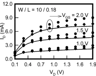
temperature and clearly indicates the hot electron phenomena near the drain edge under high bias condition VDS = VGS = 2.1 V. It takes about 40 Gummel’s iteration loops to reach the specified stop-ping criterion (maximum norm error less than 10−4). We compare the simulation validity between the HD and DD models for submicron device that chan-nel length is less than 0.25 m. By simulating a 0.18 m N-MOSFET with tox = 3.3 nm, Fig. 14
indicates there is a significant difference in I–V curves calculation between the HD (diamonds) and DD (dots) models. Compared with the measured data (lines), we find that the DD model has an over-estimation (about 25%) in ID–VD curves, whereas the HD model has more accurate simulation results. The results not only report that the HD model has good consistency with the measurement data, but also suggests that the DD model only works well for long channel MOSFETs (e.g. L = 0.25 m or
Fig. 13. Simulated electron temperature at VDS = VGS = 2.0 V in Ex. 2.
Fig. 14. Simulation and measurement of ID-VD curves for the 0.18m N-MOSFET.
above). Therefore, we confirm that the HD model plays a crucial role for the deep-submicron (short channel) MOSFETs simulation.
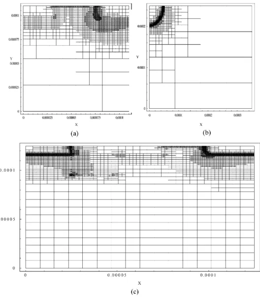
We discuss the efficiency of the adaptive simul-ation approach for N-MOSFETs simulsimul-ation. The device structure is the same as for the first example; its bias is at VDS = VGS = 2.2 V, and the problem we simulated is with the HD model. In contrast to conventional device simulation beginning with fine grids, our initial mesh contains only 16 elements and 25 nodes, so is rather simple and coarse. Start-ing with this initial mesh, the adaptive simulation automatically generates a sequence of approximated solutions on the corresponding adaptive mesh until the maximum norm error of the solution is less than a specified error tolerance. As shown in Fig. 15, the error estimation together with the error indicators here shows an efficient way of locating variations in the solutions so that the refined mesh is precisely arranged adaptively to those regions with higher errors. From the computed electrostatic potential as well as the refined mesh, shown in Figs 11 and 15(a), the adaptive method demonstrates good con-sistency and efficiency for N-MOSFET simulation. For various VLSI device simulations, the starting initial mesh for the 3.6 ⫻ 2.6 m2 P-N diode consists of 16 elements and 25 nodes, and for the 0.25 m DTMOS it consists of 256 elements and 289 nodes. Figure 15(a) shows a final refined mesh for the N-MOSFET at VDS = VGS = 2.0 V, Fig. 15(b) is for the P-N diode at applied voltage 2.0 V, and Fig. 15(c) is for the DTMOS biased at VDS = VGS = 2.0 V, respectively. All the variations of the computed solution within one element guarantee less than an error indicator, 10−4. The final P-N diode mesh consists of 2700 refined elements and
Fig. 15. Final refined mesh for various devices: (a) N-MOSFET, (b) P-N diode, (c) DTMOS.
2400 nodes. For the N-MOSFET it is 7700 elements and 7400 nodes, and for the DTMOS it is 25,100 elements and 24,000 nodes. Figure 16 shows the number of elements and nodes versus the successive adaptive refinement processes. We find that the mesh tends to have a stable refinement size after the eighth refinement level for the P-N diode and the fifteenth refinement level for both the N-MOSFET and DTMOS.
The parallel performances of the two parallel algorithms achieved are reported next. The speedup is the ratio of the code execution time on a single processor to that on multiple processors. Efficiency is defined as the speedup divided by the number of processors [43–45]. By setting a more strict error indicator 10−6 within one element, Fig. 17 shows the speedups and efficiencies of the parallel dynamic
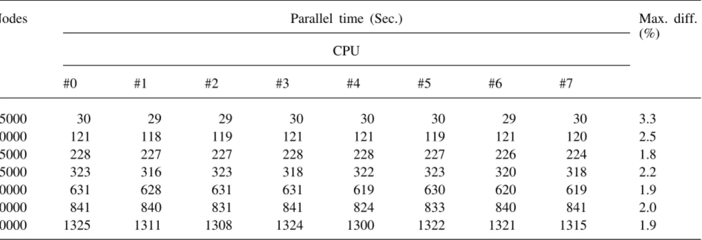
load balancing of domain decomposition for various VLSI devices on the 16 CPU Linux-cluster with the MPI library, where the applied voltage is the same as previously. The refined nodes for the P-N diode, N-MOSFET and DTMOS are 15,300, 55,600 and 60,100, respectively. Figure 18 shows the perform-ance achieved of the dynamic load balancing of domain decomposition for the N-MOSFET simul-ation. The maximum difference is defined as the maximum difference of the code execution time divided by the maximum execution time. A similar variation of the maximum difference for the P-N diode is less than 6.5%, and for the DTMOS it is 3.3%. Table 1 records the parallel load balancing timing of the DTMOS simulation on an 8-processor Linux-cluster, and it shows a good dynamic load balancing for the domain decomposition. As shown
Table 1. Parallel load balancing timing for the DTMOS simulation on an 8-CPUs Linux-cluster
Nodes Parallel time (Sec.) Max. diff.
(%) CPU #0 #1 #2 #3 #4 #5 #6 #7 5000 30 29 29 30 30 30 29 30 3.3 10000 121 118 119 121 121 119 121 120 2.5 15000 228 227 227 228 228 227 226 224 1.8 25000 323 316 323 318 322 323 320 318 2.2 40000 631 628 631 631 619 630 620 619 1.9 50000 841 840 831 841 824 833 840 841 2.0 60000 1325 1311 1308 1324 1300 1322 1321 1315 1.9
Fig. 16. Number of elements (nodes) versus refinement level for
various VLSI devices.
Fig. 17. Achieved speedups and efficiencies for the dynamic
partition of the parallel domain decomposition.
in Fig. 19, we find a nearly optimal value for the speedup and efficiency of the parallel I–V points simulation with the HD model. As partially illus-trated in Fig. 14, there are in total 11 I–V curves with VGS = 0, 0.2, %, 1.8, 2.0 V. Each one these consists of 10 I–V points, with VDS varying from 0.1 to 1.9 V with a 0.2 V step. The sequential execution time of the complete simulation of all 110 I–V points is about 21,000 seconds.
6. Conclusions
In this paper, a practical approach to implement the dynamic parallel partition for adaptive computation in semiconductor device simulation has been
Fig. 18. Load balancing of the parallel domain decomposition
Fig. 19. Speedup and efficiency of the parallel I–V points HD
simulation for the 0.18 m N-MOSFET.
presented. Using the adaptive mesh technique, FVM, error estimation and the MI method, two different parallel versions of the algorithm to perform a complete device simulation have been proposed. The first algorithm is a dynamic parallel domain decomposition approach, and the second is a parallel I–V points simulation. These two parallel simulation approaches have been shown to be an efficient alternative in parallel semiconductor device simul-ation. Combined with adaptive computing method-ology, the parallel algorithms have been developed and successfully implemented on a Linux-cluster with an MPI library. Compared with the measured data, numerical results on various VLSI devices have been presented to show the accuracy and efficiency of the method. Typical parallel perform-ance results, such as parallel speedup, efficiency, and maximum difference, have also been included. The parallel methods developed and implemented in this work show that cluster computing is a feasible alternative for characterization of semiconductor devices.
Acknowledgements
The authors express their appreciation to the referee for an exceptional in-depth reading of the manuscript. This work was supported in part by National Science Council of Taiwan under contract number NSC 90–2112-M-317–001.
References
1. Dutton, R. W., Strojwas, A. J. (2000) Perspectives on technology and technology-driven CAD. IEEE Trans. Computer-Aided Design 19(2), 1544–1560
2. Sze, S. M. (2002) Semiconductor Devices, Physics and Technology. Wiley, New York
3. Chang, C. Y., Sze, S. M. (2000) ULSI Devices. Wiley, New York
4. Yuan, J. S., Liou, J. J. (1998) Semiconductor Device Physics and Simulation. London, Plenum Press 5. Chang, S. J., Chang, C.-Y., Chao, S., Huang,
T.-Y. (2000) High performance 0.1m dynamic threshold MOSFET using indium channel implantation. IEEE Electron Devices Lett. 21(3), 127–129
6. Degond P., Ju¨ngel A., Pietra P. (2000) Numerical discretization of energy-transport models for semicon-ductors with nonparabolic band structure. SIAM J. Sci. Comput. 22(3), 986–1007
7. Li, Y., Chung, S. S., Liu, J.-L. (1999) A novel approach for the two-dimensional simulation of sub-micron MOSFET’s using monotone iterative method. Proceedings of International Symposium of VLSI Technology, Systems, and Applications, 27–30 8. Ieong, M., Tang, T.-W. (1997) Influence of
hydro-dynamic models on the prediction of submicrometer device characteristics. IEEE Trans. Electron Devices 44, 2242–2251
9. Jerome, J. W. (1996) Analysis of Charge Transport: A Mathematical Study of Semiconductor Devices. Springer-Verlag, New York
10. Chen, D., Kan, E., Ravaioli, U., Shu, C.-W., Dutton, R. W. (1992) An improved energy transport model including nonparabolicity and non-Maxwellian distri-bution effects. IEEE Electron. Devices Lett. 13(1), 26–28
11. Kerkhoven, T. (1988) A proof of convergence of Gummel’s algorithm for realistic boundary conditions. SIAM J. Numer. Anal. 23, 1121–1137
12. Hansch, W., Selberherr, S. (1987) MINIMOS 3: A MOSFET simulator that includes energy balance. IEEE Trans. Electron Devices 34, 1074–1078 13. Jerome, J. W. (1985) Consistency of semiconductor
modeling: an existence/stability analysis for the stationary van Roosbroeck system. SIAM J. Appl. Math. 45, 565–590
14. Selberherr, S. (1984) Analysis and Simulation of Sem-iconductor Devices. Springer-Verlag, New York 15. Tang, T.-W. (1984) Extension of the Scharfetter–
Gummel algorithm to the energy balance equation. IEEE Trans. Electron Devices 31(12), 1912–1914 16. Bank, R., Rose, D. J., Fichtner, W. (1983) Numerical
methods for semiconductor simulation. IEEE Trans. Electron Devices 30(9), 1031–1041
17. Bløtekjaer, K. (1970) Transport equations for electrons in two-valley semiconductors. IEEE Trans. Electron Devices 17, 38–47
18. Scharfetter, D. L., Gummel, H. K. (1969) Large-signal analysis of a silicon read diode oscillator. IEEE Trans. Electron Devices 16, 66–77
19. Gummel, H. K. (1964) A self-consistent iterative scheme for one-dimensional steady state transistor cal-culations. IEEE Trans. Electron Devices 11, 455–465 20. Li, Y., Chen, C.-K., Chen, P. (2001) Monotone iterat-ive method and adaptiterat-ive finite volume method for parallel numerical simulation of submicron MOSFET devices. In: Kluev, V. V., Mastorakis, N. E. (Editors), Topics in Applied and Theoretical Mathematics and Computer Science. WSEAS Press, 25–30
21. Li, Y., Chao, T.-S., Wang, C.-S., Sze., S. M. (2001) Monotone iterative method for parallel numerical sol-ution of 3D semiconductor Poisson equation. In: Mas-torakis, N. E., Mladenov, V., Suter, B., Wang, L. J. (Editors), Advances in Scientific Computing, Compu-tational Intelligence and Applications. WSES Press, 54–59
22. Garcia-Loureiro, A. J., Pena, T. F. (1999) Parallel domain decomposition applied to 3D simulation of gradual HBTs. J. Modeling & Simulation of Microsyst. 1(2), 115–120
23. Antonoiu G., Dima G., Profirescu M. D. (1998) Paral-lel domain decomposition for 3D semiconductor device simulation. Proceedings of International Sem-iconductor Conference, 2, 371–374
24. Aluru, N. R., Law, K. H., Dutton, R. W. (1996) Simul-ation of the hydrodynamic device model on distributed memory parallel computers. IEEE Trans. Computer-Aided Design 15(9), 1029–1047
25. Tanaka K., Ciampohni P., Pierantoni A., Baccarani G. (1993) Comparison between a posteriori error indi-cators for adaptive mesh generation in semiconductor device simulation. Proceedings of International Work-shop on VLSI Process and Device Modeling, 118–119 26. Coughran, W. M., Jr., Pinto, M. R., Smith, R. K. (1991) Adaptive grid generation for VLSI device simulation. IEEE Trans. Computer-Aided Design 10(10), 1259–1275
27. Burgler, J. F., Coughran, W. M., Jr., Fichtner, W. (1991) An adaptive grid refinement strategy for the drift-diffusion equations. IEEE Trans. Computer-Aided Design 10(10), 1251–1258
28. Sharma, M., Carey, G. F. (1989) Semiconductor device simulation using adaptive refinement and flux upwind-ing. IEEE Trans Computer-Aided Design 8(6), 590– 598
29. Teresco, J. D., Beall, M. W., Flaherty, J. E., Shephard, M. S. (2000) A hierarchical partition model for adapt-ive finite element computation. Comput. Meth. Appl. Mech. Eng. 184(2–4), 269–285
30. Bank, R. E., Holst, M. (2000) A new paradigm for parallel adaptive meshing algorithms. SIAM J. Sci. Comput. 22(4), 1411–1443
31. Zhang, X. D., Tre´panier, J.-Y., Camarero, R. (2000) A posteriori error estimation for finite-volume sol-utions of hyperbolic conservation laws. Comput. Meth. Appl. Mech. Eng. 185(1), 1–19
32. Lages, E. N., Paulino, G. H., Menezes, I. F. M., SilvaNonlinear, R. R. (1999) Finite element analysis using an object-oriented philosophy-application to beam elements and to the cosserat continuum. Eng. With Comput. 15(1), 73–89
33. Oden, J. T., Patra, A., Feng, Y. (1997) Parallel domain decomposition solver for adaptive hp finite element nethods. SIAM J. Numer. Anal. 34(6), 2090–2118 34. Galloue¨t, T., Herbin, R., Vignal, M. H. (2000) Error
estimates on the approximate finite volume solution of convection diffusion equations with general boundary conditions. SIAM J. Numer. Anal. 37(6), 1935–1972 35. Ramakrishnan, R. (1994) Structured and unstructured
grid adaptation schemes for numerical modeling of field problems. Appl. Numerical Math. 14(1–3), 285–310
36. Whiteman, J. R. (1994) The Mathematics of Finite Elements and Applications. Wiley, New York 37. Bank, R. E., Rose, D. J. (1987) Some error estimates
for the box method. SIAM J. Numer. Anal. 24(4), 777–787
38. Babuska, I., Rheinboldt, W. C. (1978) Error estimates for adaptive finite element computation. SIAM J. Numer. Anal. 15, 736–754
39. Babuska, I., Rheinboldt, W. C. (1978) A-posteriori error estimates for the finite element method. Int. J. Numer. Meth. Eng. 12, 1597–1615
40. Li, Y. (2002) A monotone iterative method for sem-iconductor device drift diffusion equations. WSEAS Trans. Syst. 1(1), 68–73
41. Pao, C. V. (1995) Block monotone iterative methods for numerical solutions of nonlinear elliptic equations. Numerische Mathematik 72(02), 239–262
42. Heikkila, S., Lakshmikantham, V. (1994) Monotone Iterative Techniques for Discontinuous Nonlinear Dif-ferential Equations. Marcel Dekker, New York 43. Gropp, W., Lusk, E., Thakur, R. (1999) Using
MPI-2: Advanced Features of the Message-Passing Inter-face. MIT Press, Cambridge, MA
44. El-Rewini, H., Lewis, T. G. (1998) Distributed & Parallel Computing. Manning, Greenwich, NY 45. Pacheco, P. S. (1997) Parallel Programming with MPI.
Morgan Kaufmann, San Francisco, CA
46. Varga, R. S. (2000) Matrix Iterative Analysis. Springer-Verlag, New York
47. Li, R., Chen, Z., Wu, W. (2000) Generalized Differ-ence Methods for Differential Equations: Numerical Analysis of Finite Volume Methods. Marcel Dekker, New York
48. Versteeg, H. K., Malalasekera, W. (1995) An Intro-duction to Computational Fluid Fynamics: the Finite Volume Method. Addison Wesley Longman, Harlow, Essex
49. Crumpton, P. I., Mackenzie, J. A., Morton, K. W. (1993) Cell vertex algorithms for the compressible Navier-Stokes equations. J. Computational Phys. 109, 1–15