This content has been downloaded from IOPscience. Please scroll down to see the full text.
Download details:
IP Address: 140.113.38.11
This content was downloaded on 26/04/2014 at 04:38
Please note that terms and conditions apply.
Optical properties of In0.3Ga0.7N/GaN green emission nanorods fabricated by plasma
etching
View the table of contents for this issue, or go to the journal homepage for more
2007 Nanotechnology 18 335706
(http://iopscience.iop.org/0957-4484/18/33/335706)
Nanotechnology 18 (2007) 335706 (4pp) doi:10.1088/0957-4484/18/33/335706
Optical properties of In
0
.
3
Ga
0
.
7
N/GaN
green emission nanorods fabricated by
plasma etching
C H Chiu
1, M H Lo
1, C F Lai
1, T C Lu
1,5, H W Huang
1,2,
Y A Chang
1, T H Hsueh
1, C C Yu
1, H C Kuo
1,5, S C Wang
1,
C F Lin
3and Y K Kuo
41Department of Photonics, National Chiao Tung University, Hsinchu 300, Taiwan, Republic
of China
2TrueLight Corporation, Hsinchu 300, Taiwan, Republic of China
3Department of Materials Engineering, National Chung Hsing University, Taichung 402,
Taiwan, Republic of China
4Department of Physics, National Changhua University of Education, Changhua 500, Taiwan,
Republic of China
E-mail:[email protected]@faculty.nctu.edu.tw
Received 3 April 2007, in final form 4 June 2007
Published 25 July 2007
Online at
stacks.iop.org/Nano/18/335706
Abstract
In this study, we have fabricated In
0.3Ga
0.7N/GaN green emission nanorods
and demonstrated optical enhancement by photoluminescence (PL)
measurements. An enhancement factor of 3.5 and an emission peak blue-shift
of 6.6 nm were observed at 300 K for the green emission nanorods structure
in comparison to the as-grown flat surface structure. The blue-shift
phenomenon from the nanorod structure could be caused by a partial
reduction of the internal piezoelectric field. However, the similar carrier
decay time for the green emission nanorod structure and the as-grown flat
surface structure observed in low-temperature time-resolved PL
measurements indicates that the dominant optical enhancement mechanism
of the green emission nanorod structure could be mainly resulting from the
large emission surface areas and the multiple scattering paths between the
nanorods.
(Some figures in this article are in colour only in the electronic version)
GaN-based nitride semiconductors have attracted much attention for applications in optoelectronic devices in the visible light region [1]. In particular, InGaN/GaN multiple quantum wells (MQWs) have been used as the active layers for optical devices such as light-emitting diodes (LEDs) and laser diodes [2–4]. Recent reports have indicated the InGaN/GaN nanostructures can exhibit optical and electrical properties that are different from those in the bulk material. The nanostructures could result in the enhancement of photoluminescence (PL) intensity. Recently, by the rapid development of fabrication methods for nanostructures, fabricating nanostructures like quantum dots or quantum wires
5 Authors to whom any correspondence should be addressed.
on the surface is feasible. For nanoscale GaN-based structures, until now, several GaN-based nanostructures have been produced by various fabrication methods, such as inductively coupled plasma reactive-ion etching (ICP-RIE) without a mask [5], synthesis using carbon nanotubes as templates [6], and the growth of single-crystal GaN nanorods by hydride vapor-phase epitaxy [7]. The growth of GaN nanorods by using ferrocene as the catalyst, i.e. the so-called vapor–liquid– solid (VLS) mechanism, was also demonstrated [8]. However, all of these reported methods are relatively complicated, and their resulting structures without active layers are not quite appropriate for optoelectronic device applications.
Recently, we have reported the fabrication of InGaN/GaN MQW blue emission nanorods by using nanometer-sized
Nanotechnology 18 (2007) 335706 C H Chiu et al
nickel (Ni) islands as etching masks. These nanosize Ni islands were formed by choosing the appropriate initial Ni thickness, annealing temperature, and annealing time [9]. However, the optical properties of InGaN/GaN MQW green nanorod structures have not been fully studied yet since the higher In content in thec-plane MQW could result in lower emission efficiency due to the strong quantum confined Stark effect. In this report, we present the results of enhanced emission intensity properties of InGaN/GaN MQW green emission nanorods and analyze the dominant enhancement mechanism using temperature-dependent PL, time-resolved photoluminescence (TRPL) and a theoretical simulation.
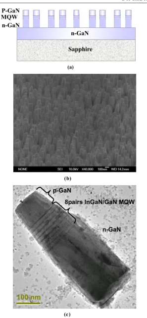
The samples were grown by metal-organic chemical vapor deposition with a rotating-disk reactor on a c-plane sapphire (0001) substrate at the growth pressure of 200 mbar. The structure consists of a 50 nm thick GaN nucleation layer, a 3 µm thick Si-doped n-GaN buffer layer, an unintentionally doped In0.3Ga0.7N/GaN MQW active region, and a 0.1µm
thick Mg-doped p-GaN. The MQW active region consists of eight periods of 7 nm/15 nm thick In0.3Ga0.7N/GaN well
layers and barrier layers. The grown sample was then subjected to induction coupled plasma etching under Ar/Cl2
ambient gases. The detailed process conditions of nanorods have been reported elsewhere [9]. A schematic diagram of fabricated In0.3Ga0.7N/GaN MQWs nanorods is shown in
figure 1(a). Figures 1(b) and (c) show the tilted 45◦ field-emission scanning electron microscope (Hitachi, FE-SEM S-5000) image and transmission electron microscope (JEOL, JEM-200CX) image of the fabricated In0.3Ga0.7N/GaN MQWs
nanorods, respectively. The dimension and density of the nanorods were estimated from the SEM image to be around 550 nm and 3×109 cm−2, respectively. The etching depth estimated from the TEM image is about 0.6µm. In figure1(c), eight pairs of In0.3Ga0.7N/GaN MQWs of 7 nm/15 nm thick
In0.3Ga0.7N/GaN well layers and barrier layers embedded
within the nanorod can be clearly observed. The In percentage of the QWs was obtained from the fitting results of the x-ray measurement data. The optical properties of the nanorods were studied by PL at temperatures between 20 and 300 K, and by TRPL at 10 and 300 K. For the PL measurement, the nanorod samples were excited by a 325 nm He–Cd laser with an excitation power of 25 mW and the emitted luminescence light was collected through a 0.32 m spectrometer with a charge-coupled device detector. The focused spot size of the He–Cd laser was estimated to be about 200 µm in diameter. The TRPL measurements were carried out using a second-harmonic pulsed Ti:sapphire laser at a wavelength of 400 nm and a time-correlated single photon counting detection system. The power density of the pumped beam in the TRPL measurement was about 1 kW cm−2.
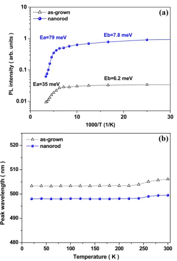
Figure 2(a) shows an Arrhenius plot of the integrated PL intensity obtained from the In0.3Ga0.7N/GaN MQW active
layer emission of the as-grown sample and the nanorod sample over the temperature range from 20 to 300 K. The results indicate that the PL intensity of the nanorods is stronger than that of the as-grown sample by a factor of approximately 3.5 at room temperature. Such large emission enhancement could result from improvement either in internal quantum efficiency or external extraction efficiency. The temperature-dependent data of figure 2(a) were fitted with the following formula:
Figure 1. (a) A schematic diagram of the In0.3Ga0.7N/GaN MQW
green nanorod structure. (b) Tilted 45◦SEM and (c) TEM images of
In0.3Ga0.7N/GaN MQW green nanorods.
IT = I0/[1+ Aexp(−Ea/kT )+ Bexp(−Eb/kT )], whereIT,
I0are the integrated PL intensity forT and 0 K, Aand Bare
constants,k is the Boltzmann constant,T is the temperature,
Ea is the activation energy for PL quenching, and Eb is
generally associated to the free exciton binding energy [10]. The energy Eb of the as-grown and nanorod samples was
approximately 6.2 and 7.8 meV, respectively, which was similar to values in the previous report [11]. However, the activation energy Ea of as-grown and nanorod samples was
35 and 79 meV, respectively. Though the high surface ratio around the periphery of the nanorods could provide many non-radiative recombination paths, the larger activation energy of the nanorods obtained seems to suggest that there are higher potential barriers in the nanorods for carriers, where they could easily localize in the effective potential minima of the nanorod structures [12]. Figure2(b) compares the PL peak emission energy of the as-grown sample and nanorod sample measured from 20 to 300 K. The PL emission peak 2
Figure 2. (a) An Arrhenius plot of the integrated PL intensity
obtained from the In0.3Ga0.7N/GaN MQW active layer emission over
the temperature range from 20 to 300 K. (b) Comparing the PL spectra from as-grown and green emission nanorods excited by a 325 nm He–Cd laser from 20 to 300 K.
of as-grown and nanorod samples are 503.3 and 498 nm at a temperature of 20 K and 506.1 nm and 499.5 nm at room temperature, respectively. A blue-shift of the emission peaks from the nanorods in comparison to the as-grown sample can be observed. Since the 100 nm diameter of the nanorod is too large to result in the quantum confinement effect, the blue-shift of the nanorod emission peak from that of the as-grown sample could be caused by the partial reduction of the piezoelectric (PZ) field in the nanorod. The blue-shift of 6.6 nm (32.5 meV) at the temperature of 300 K corresponds to the reduction in the piezoelectric field caused by the partial strain release, the reduction of the internal field in a quantum well was obtained to be around 32.5 mV/7 nm=0.05 MV cm−1, where 7 nm is the well thickness. A larger wavelength red-shift of as-grown samples, 2.8 nm (13.6 meV), than that of the nanorod samples, 1.5 nm (7.4 meV), was clearly observed as the temperature increased from 20 to 300 K, indicating that possible strain relaxation occurred in the nanorod samples. Therefore the reduction of the internal PZ field could account for part of the reasons for the blue-shift of the PL emission peak.
Figure 3 shows the carrier lifetime from the as-grown and nanorod samples measured by TRPL at 10 and 300 K respectively. Since a purely radiative recombination at T =
10 K can be assumed [13], the radiative lifetime of the
Figure 3. TRPL lifetime curves of the In0.3Ga0.7N/GaN MQW as-grown and green emission nanorod samples for the main InGaN emission peak measured at 10 and 300 K.
nanorod sample is similar to that of the as-grown sample, which is approximately 54 ns, indicating that the radiative recombination process for both samples is similar and the internal field reduction in the nanorods sample plays a minimal role in the emission enhancement. As the temperature increased to 300 K, the carrier lifetimes were further shortened to 8.7 and 16.5 ns for the nanorod and as-grown samples due to the increase of the non-radiative recombination rate in the nanorod structures. The relatively larger non-radiative recombination rate at room temperature for the nanorod sample was probably due to the increasing surface recombination around the periphery of the nanorod. Generally, reduction of the internal PZ field facilitates a better wavefunction overlapping of electrons and holes in the green emission nanorod MQWs that could result in the increase of the emission efficiency and enhancement in the PL emission intensity of the nanorods. However, the PRTL measurement results reveal that the reduction of the internal PZ field could not be large enough to enhance the radiative recombination process in the green emission nanorods. As a result, the internal quantum efficiency of the nanorod sample at room temperature could not be improved, indicating that the PL intensity enhancement observed from the nanorod sample could result from the increased emission surface of the nanorod structure.
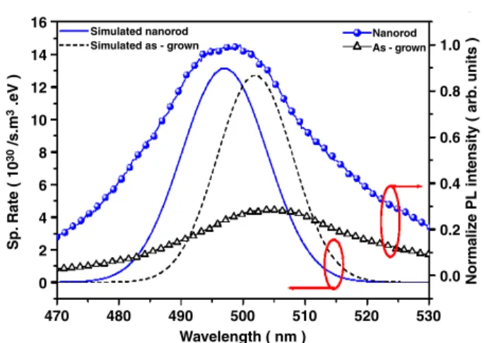
To verify the impact of the reduction of the internal field in the InGaN/GaN green emission MQWs on the radiative recombination process, we further calculate the spontaneous emission rate from the InGaN quantum well with different internal fields using a commercially available advanced physical model of semiconductor devices (APSYS) software [14]. In the gain model, the material gain and loss for both the bulk and the QW as functions of wavelength and carrier density are computed with material-dependent parameters [15] and the default database values given in the APSYS material macro file [10], and the gain spectral functions are widened by including the many-body Coulomb interaction. The calculation of the interface charge density including spontaneous and piezoelectric polarization in the ternary III-nitride material as a function of composition and microscopic structure is based on ab initio density-functional
Nanotechnology 18 (2007) 335706 C H Chiu et al 16 14 12 10 8 Sp. Rate ( 10 30 /s.m 3 .eV ) 6 4 2 0 470 480 490 500 Wavelength ( nm ) 510 520 530 1.0 0.8 0.6 Normaliz e PL intensity ( arb. units ) 0.4 0.2 0.0 Simulated nanorod Simulated as - grown Nanorod As - grown
Figure 4. Solid and dashed curves are the radiative recombination
rates of the structures with two different polarization charges in the
In0.3Ga0.7N/GaN QW. The solid curves with symbols are the
measured PL spectra for the nanorods and as-grown flat surface structures at 300 K.
techniques and Berry phase method [16]. In the simulation, a simple structure that consists of a single 7 nm thick In0.3Ga0.7N QW and two 15 nm thick GaN barrier, which
are sandwiched between 2µm thick n-type GaN and 100 nm thick p-type GaN, is assumed for the discussion of the strain relaxation effect. The band tiling of the QW may have strong consequences on the carrier distribution and affects the output device characteristics. Figure 4 shows the radiative recombination rates of the structures with the two different polarization charges in a single QW. In the calculation, we assumed that the charges at the single QW were with partial 33% screening and partial 20% screening, representing the different internal field conditions of the QW in our nanorod and as-grown samples, respectively. The carrier density in the MQW structure was 1.7×1018cm−3, which is similar to the
carrier density generated in our optical pumping experiment. The calculation results show that the spontaneous emissions at 502 and 510 nm for simulated nanorod and as-grown samples were of similar magnitude, which is the same as the low-temperature TRPL result. Since this simulation did not take into account the non-radiative recombination, the radiative recombination rate is similar even for these two different internal fields in QW structures. This calculation indicates that the internal field existing in such a 7 nm thick In0.3Ga0.7N QW
was relatively large, such that partial relaxation by formation of nanorods did not improve the radiative recombination rate to a significant extent. As a result, the enhanced PL intensity of the nanorod sample measured at room temperature shown in figure4could be mainly resulting from the increased light extraction efficiency from the large emission surface areas and the multiple scattering paths between nanorods.
In conclusion, we have investigated the optical properties of InGaN/GaN MQW green emission nanorods fabricated by
inductively coupled plasma etching using a Ni nanomask. An increase in the PL emission intensity of the nanorod by 3.5 times over that of the as-grown sample was measured. A blue-shift of 32.5 meV in the nanorod PL emission peak from that of the as-grown sample was observed and attributed to a partial reduction of the piezoelectric field. However, since the radiative recombination rates were similar from the low-temperature TRPL results and the simulation results for the InGaN/GaN MQW green emission nanorods and as-grown sample, the enhancement of PL intensity from the green emission nanorods could be mainly due to the increased light extraction efficiency from the nanorods. The large surface area of the nanorods results in not only enhancing the sidewall scattering between each nanorod, but also providing a route to enhance the optical absorption. Both effects lead to the PL intensity of nanorods sample being increased.
Acknowledgments
This work was supported in part by the National Science Council of the Republic of China (ROC) in Taiwan under Contract No. NSC95-2120-M-009-008 and by the Academic Excellence Program of the ROC Ministry of Education under Contract No. NSC95-2752-E-229-007-PAE.
References
[1] Nakamura S 1998 Science281 956
[2] Mukai T, Yamada M and Nakamura S 1999 Japan. J. Appl.
Phys. 138 3976
[3] Nakamura S, Senoh M, Nagahama S, Iwasa N, Yamada T, Matsushita T, Kiyoku H and Sugimoto Y 1996 Japan. J.
Appl. Phys. 235 L74
[4] Akasaki I, Sota S, Sakai H H, Tanaka T, Koike M and
Amano H 1996 Electron. Lett.32 1105
[5] Yu C C, Chu C F, Tsai J Y, Huang H W, Hsueh T H,
Lin C F and Wang S C 2002 Japan. J. Appl. Phys. 141 910
[6] Han W Q, Fan S S, Li Q Q and Hu Y D 1997 Science277 1287
[7] Kim H M, Kim D S, Kang T W, Cho Y H and Chung K S 2002
Appl. Phys. Lett.81 2193
[8] Han W Q and Zettl A 2002 Appl. Phys. Lett.80 303
Chen H S, Yeh D M, Lu Y C, Chen C Y, Huang C F, Tang T Y, Yang C C, Wu C S and Chen C D 2006 Nanotechnology 17 1454
[9] Huang H W, Kao C C, Hsueh T H, Yu C C, Lin C F, Chu J T,
Kuo H C and Wang S C 2004 Mater. Sci. Eng. B113 125
[10] Yu C C, Chu C F, Tsai J Y, Lin C F and Wang S C 2002
J. Appl. Phys.92 1881
[11] Lai Y L, Liu C P, Lin Y H, Lin R M, Lyu D Y, Peng Z X and
Lin T Y 2006 Appl. Phys. Lett.89 151906
[12] Cho Y H et al 2003 Appl. Phys. Lett.83 2578
[13] Deleporte E, Martinez-Pastor J, Filoramo A, Batovski D, Roussignol Ph, Delalande C, Morhain C, Tourni´e E and
Faurie J P 1995 Nuovo Cimento17 1436
[14] APSYS User’s Manual, Crosslight Inc. Software, Canada.
Available online at web pagehttp://www.crosslight.ca
[15] Chang Y A, Yen S H, Wang T C, Kuo H C, Kuo Y K,
Lu T C and Wang S C 2006 Semicond. Sci. Technol.21 598
[16] Bernardini F and Fiorentini V 2002 Phys. Status Solidi a 190 65