國 立 交 通 大 學
光電工程研究所
碩 士 論 文
噴墨列印技術於彩色濾光片製程之應用
Ink-Jet Printing Technology in
Color Filter Fabrication
研 究 生 : 施佑儒
指 導 教 授 : 陳皇銘
噴墨列印技術於彩色濾光片製程之應用
Ink-Jet Printing Technology in
Color Filter Fabrication
研 究 生 : 施 佑 儒
Student : Shin You-Ru
指 導 教 授 : 陳 皇 銘
Advisor : Huang-Ming Philip Chen
國 立 交 通 大 學
光 電 工 程 研 究 所
碩 士 論 文
A Thesis
Submitted to Institute of Electrical-Optical College of Electrical Engineering and Computer Science
National Chiao-Tung University in Partial Fulfillment of the Requirements
for the Degree of Master
in
Institute of Electrical-Optical July 2007
Hsinchu, Taiwan, Republic of China.
噴墨列印技術於彩色濾光片製程之應用
研究生: 施佑儒 指導教授: 陳皇銘 博士
國立交通大學光電工程研究所
摘要
近年來,平面顯示器產業技術(LCD、OLED、PDP、FED等)已趨成熟,很多公 司及研究單位紛紛投入下一世代顯示器的開發。彩色濾光片是液晶顯示器的關鍵零組 件,目前彩色濾光片以旋轉塗佈法製程為主流,但旋轉塗佈法在成本考量上十分浪費, 且其製程步驟繁複、重複。另外旋轉塗佈法對於下一世代的面板(超大型基板)製程較不 適用。 利用噴墨列印技術,可以精確地列印出彩色濾光片所需的紅、綠、藍三原色畫素陣 列,並且噴墨列印技術以最少材料、最環保製程製作顯示器的彩色濾光片。但在利用此 項技術上,為防止彩色顏料在噴印過程中,由於墨水高度可能要比黑色矩陣來的高出許 多,而因此造成墨水溢流,並且互相混色的情形。因此本論文根據墨水特性對於黑色矩 陣基板做相應的處理,將墨滴在黑色矩陣的接觸角提高,使墨滴黑色矩陣牆上不濕潤, 用以避免混色情形在噴墨列印過程中發生。本論文共使用兩種方法用以使墨滴黑色矩陣 牆上不濕潤上,作為參考,並討論其表面特性的改變以及其他效應的產生,進一步說明 此二種方法在實際噴塗的應用性。 本論文並且使用顯示科技所財產下的噴墨列印系統,實際進行噴塗,完成紅、綠、 藍三色的單色噴塗,並將三色整合噴塗於黑色矩陣基板上,完成擁有紅、綠、藍三原色 畫素陣列。Ink-Jet Printing Technology in
Color Filter Fabrication
Student: Shin You-Ru Advisor: Dr. Huang-Ming Philip
Chen
Institute of Electrical-Optic
National Chiao Tung University
Abstract
The color filter (CF) has been one of the most important components for full-color active matrix LCD panel. An emerging process for manufacturing CF has been technically developed by an inkjet printing system. Inkjet printing process for color filter fabrication is key technology for next generation process.
To prevent ink overflow from the black matrices (BM) bank, two effective surface treatments are introduced in this thesis. Because the color ink is jetting on glass substrates with black matrices (BM), the total jetting droplet’s volume will overflow from one bank to another if the volume is much larger than the bank. Increase contact angle of drops on BM to make color ink not wetting and to prevent ink overflow from the BM bank. The contact angle of drops on chemical treated and CFx plasma treated BM are increased.
In this thesis, we also use the Litrex 70L ink-jet printing system to print red, green, and blue single color films. And we also combined the red, green, and blue color films to form a three-color films BM.
誌謝
隨著畢業季節的到來,回想兩年來的學習,要感謝非常多的人。首先要感謝我的 指導教授陳皇銘博士,在不管是學業和實驗上,不辭辛勞的給我鼓勵和指導,終有這 篇論文的產生,使我受益良多。 另外我更要感謝鄭榮安博士對我的指導,能夠在我的實驗進行不順,而我茫然無 知時,給我許多的意見與資源,並能在我毫不熟悉的領域上,給我幫忙和動力,使我 從一個無知的小碩一,直至今日能有一些小成果。另外我也要感謝學弟祥志,幫我分 擔了許多實驗上許多瑣碎的事情,也一直陪著我做實驗、搞機台,並且也能在實驗上 互相討論,完成此篇論文。 在此我還要感謝實驗室的各位,坤展、威慶、耿睿、俊民、耀慶、佳恬、鴻杰, 一起同甘共苦,一起打拼課業,並且能在實驗上,一起討論,還有學長書豪、世民、 宜揚陪著我努力、嘻笑,也非常謝謝各位學弟妹,文孚、彣綺、怡帆、謹瑋、蓮馨, 幫大家一起做實驗,為這個實驗室貢獻,大家可以說是好夥伴,希望以後也還能常常 聯絡。 另外也要感謝工程師林育欣的幫忙,沒有你我們大家也搞不定實驗機台,更要對 這些日子來,帶給你的麻煩說聲抱歉。總之要感謝的人太多太多了,在這裡佑儒對你 們致上最高的感謝之意,謝謝。Table of contents
Chinese abstract ……….. i English abstract ………... ii Acknowledgement ………... iii Table of contents ……….………... iv List of Figures ……… vi List of Tables ……… ix Chapter 1 Introduction 1.1 Introduction of LCD structure……… 1 1.2 Color filter of LCD………. 21.3 Color filter conventional fabrication……….………. 3
1.4 Introduction of ink-jet printing………..………. 4
1.5 Advantage of IJP……...……….………. 7
1.6 IJP in color filter fabrication………...……… 7
Chapter 2 Surface treatment 2.1 Surface treatment in IJP color filter application ……… 9
2.2 Chemical surface treatment………. 10
2.3 Plasma surface treatment……….………...……... 11
Chapter 3 Experiment 3.1 Experiment design….………..………..………. 14
3.2 Ink characterizations of IJP………. 16
3.2.1 Ink property………. 16
3.2.2 Color film property………. 18
3.2.3 Color film reliability………... 19
3.3 BM glass treatment………...……….. 21
3.3.1 BM glass chemical treatment……….. 21
3.3.2 BM glass plasma treatment………. 21
3.3.3 Ink contact angle measurement………... 22
3.4 Printing process………... 23
3.4.2 Printing process & maintain……… 24
Chapter 4 Result & Discussion 4.1 Contact angle of BM glass surface treatment………. 26
4.1.1 Contact angle of BM glass chemical surface treatment……….. 27
4.1.2 Contact angle of BM glass CFx plasma surface treatment 30 4.1.3 Discussion of surface energy 34 4.2 Printed R G B single color film…... 35
4.2.1 Printed Red single color film……….. 36
4.2.2 Printed Green single color film………... 38
4.2.3 Printed Blue single color film………. 40
4.3 Printed R G B color film………..………... 41
4.4 Summary………. 42
Chapter 5 Conclusions & Future Works 5.1 Conclusions……..………... 44
5.2 Future Works………... 45
List of Figures
Fig.1.1. Basic structure and components of LCD display panel and its work
function……….. 2
Fig.1.2. Color filter structure of RGB color films and BM on the glass substrate………...……….. 2
Fig.1.3. Color filter conventional fabrication……….…… 3
Fig.1.4. Ink-jet printing technology tree……….……… 5
Fig.1.5. Thermal bobble print head……….… 6
Fig.1.6. Piezoelectric print head (Shear mode)………...……… 6
Fig.2.1. Monolayer chemical formed on the substrate……… 11
Fig.2.2. Principle of plasma generation using Ar as an example……… 12
Fig.2.3. Effect of plasma in the chamber………...………. 13
Fig.3.1. Litrex 70 ink-jet printer………...……….. 14
Fig.3.2. Basic structure of ink jet printing system……..……… 15
Fig.3.3. The relationship of drop size and drop diameter for a spherical shape drop……….………...… 16
Fig.3.4. (a) Shear for fluid by Newton (b) BROOKFIELD/U.S.A DV-III+ viscosity measurement instrument……… 17
Fig.3.5. (a) RGB Color film thickness and roughness (b) UV-visible spectrum of RGB color film……….……….. 19
Fig.3.6. UV-visible spectrum of RGB color film and CIE1931 color coordinate of chemical resistance tests……… 20
Fig.3.7. Chemical treatment process………... 21
Fig.3.8. Plasma treatment process………... 22
Fig.3.9. Method of contact angle system measurement (a) wetting surface (b) not wetting surface……….………….. 22
Fig.3.10. Design for one of the three primary color print pattern using Litrex inside program ………...………. 23
Fig.3.11. Every subpixel are designed to print 7 drops………. 24
Fig.3.12. The mechanical langrage which is called swath and the printing recipe………...……... 24
Fig.3.13. Drops jetting out of the nozzle (a) earlier time of drops jetting out of the nozzle (b) later time of drops jetting out of the nozzle………. 25
Fig.4.1. Contact angle of water on blank BM………. 26
Fig.4.2. Contact angle of water on different treatment BM and glass………...…. 27
Fig.4.3. Contact angle of red ink drop on blank BM and glass (a) blank BM (b)blank glass………...……… 27
Fig.4.4. Contact angles of red ink drops on (a) chemical1 treated BM (b) chemical1
treated glass(c) chemical2 treated BM (d) chemical2 treated glass……….. 28
Fig.4.5. Contact angle of green ink drop on blank BM and glass (a) blank BM (b)blank
glass………... 28
Fig.4.6. Contact angles of green ink drops on (a) chemical1 treated BM (b) chemical1
treated glass(c) chemical2 treated BM (d) chemical2 treated glass... 29
Fig.4.7. Contact angle of blue ink drop on blank BM and glass (a) blank BM
(b)blank... 29
Fig.4.8. Contact angles of blue ink drops on (a) chemical1 treated BM (b) chemical1
treated glass(c) chemical2 treated BM (d) chemical2 treated glass……….. 30
Fig.4.9. Red ink drops on CFx plasma treatment (a) BM side (b) and glass
side.………...……. 31
Fig.4.10. Green ink drops on plasma treatment (a) BM side (b) and glass
side…..….………..… 31
Fig.4.11. Blue ink drops on plasma treatment (a) BM side (b) and glass
side. ………... 32
Fig.4.12. Height of BM with the treatment time increasing for 0 to 50
seconds………...…….. 33
Fig.4.13. Contact angles of red ink drops on different time plasma treatment BM (a1) 10s
(b1) 20s (c1) 30s and glass (a2) 10s (b2) 20s (c2) 30s……….. 34
Fig.4.14. Drops on chemical treated BM by dip coating………... 35 Fig.4.15. The printed red color film observed under POM………... 36 Fig.4.16. The profile of red color film and the thickness of color film are about 0.1 um
measuring by α-step...……….. 36
Fig.4.17. UV-visible spectrum of single red color film for film thickness 0.1
um……….………. 37
Fig.4.18. Different printing times of color film thickness (a) film profile (b) OM
picture……… 37
Fig.4.19. The printed green color film observed under POM………... 38 Fig.4.20. The profile of green color film and the thickness of color film are about 0.1 um
measuring by α-step………...………... 39
Fig.4.21. UV-visible spectrum of single green color film for film thickness 0.1
um………...…. 39
Fig.4.22. The printed blue color film observed under POM………. 40 Fig.4.23. The profile of blue color film and the thickness of color film are about 0.2 um
measuring by α-step………. 40
Fig.4.25. RGB color filter observed under POM……….. 41 Fig.4.26. The profile of RGB color films……….. 42
List of Tables
Table.1.1. Compare with ink-jet print and conventional color filter process………... 8
Table.3.1. Specification of print head………...…... 16
Table.3.2. Ink and color film properties……….………...…... 17
Chapter 1
Introduction
1.1 Introduction of LCD structure
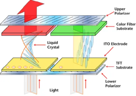
Following with the multimedia age, the huge growth of liquid crystal display (LCD) has been exhibited by the vital requirement of market for the application of flat panel display in the field of portable, consumer, and information technology oriented commodities. Small applications include portable devices, such as mobile phones, digital cameras, handheld games, PDAs and GPS. For large applications, LCD technology aggressively fits into all branches, such as laptop screens, monitors, TV and high-definition TV (HDTV). As we know, LCD is combined with the three most important part of light source like CCFL, LED and gray scale control including LC, polarizer, TFT with driver IC and color filter to reach full color display.
TFT is used for generating an electric field to control the liquid crystal orientation. The polarized light will have different retardations when passing through the different orientation liquid crystal layer. The gray scale is controlled by using two polarizers and different polarized light for LCD display as shown in Fig. 1.1. Color filter of red, green, and blue subpixel is used for full color LCD display.
Fig. 1.1 Basic structure and components of LCD display panel and its work function
1.2 Color filter of LCD
The color filter has been one of the most important devices for full-color active matrix LCD panel since it obviously defines the image quality of flat panel display in chromatic characteristics [4][7].
Fig. 1.2 Color filter structure of RGB color films and BM on the glass substrate
It is formed by arranging coloring materials on each pixel to selectively transmit the three primary colors (red, green, and blue) of light as shown in Fig. 1.2 [27][28][29]. The
device and line sensor of crystal shutter [3].
1.3 Color filter conventional fabrication
Various color filter production processes have been developed to reduce the cost of the color filter. Two typical color filter production processes are as follows. The first conventional process is a dyeing process. A water-soluble polymer for dyeing is sensitized by adding a photosensitive material. Then, the sensitized polymer is patterned into a desired shape on a transparent substrate by photolithography, and the pattern is dyed in a dyeing bath to produce a colored pattern. This operation is repeated three times to produce a color filter. On the other hand, the second conventional process is a pigment dispersion process [7]. Currently this process is widely used for mass production. A photosensitive resin layer containing a dispersed pigment is formed on a substrate. The resin layer is patterned to obtain the pixel pattern by lithography. This operation is repeated three times to establish an RGB color filter as shown in Fig. 1.3. The above two processes require repeating the same operation three times for the formation of R, G and B pixels, thereby increasing the production cost. Moreover, the yield decreases with increasing number of steps.
1.4 Introduction of ink-jet printing
The earliest development of ink-jet printing was in 1878. After 1951, Siemens Company published a patent of turning ink into drops technology. Year 1964, the volume of drop and printing speed could be controlled by using a special machine; this is the basic mechanism of ink-jet printing. Until to 1967, Hertz Company developed the ink-jet printer of continuous type, it’s now the continuous ink-jet printing technology of industry manufacturing. Year 1972, Siemens Company published piezoelectric type of Drop-on-Demand ink-jet printing. Year 1979, Canon published thermal type of Drop-on-Demand ink-jet printing and made a name of Bubble Ink-jet Printing. Year 1984, HP also published thermal type of Drop-on-Demand ink-jet printing. Those are the history of ink-jet printing technology [9][10].
Basically, there are two types of ink-jet printing. First one is continuous type, the others is Drop-on-Demand type. Continuous type is majored in industry manufacturing without high resolution. The advantages of continuous type including high printing speed, smooth of printed surface is not so important. But continuous type has the disadvantage of low resolution. Continuous type ink-jet printing is usually used for printing large playbill, large billboard… etc.
Drop-on-Demand type is different from continuous type, the print speed is not so fast but Drop-on-Demand ink-jet printing has very high resolution, though the printed surface would be very flat.
There are thermal 、 piezoelectric 、 electrostatic 、 acoustic, four kinds of Drop-on-Demand ink-jet printing type as shown in Fig 1.4. The first tow kinds is principally developed and used [11][12].
Fig. 1.4 Ink-jet printing technology tree
Thermal ink-jet printing is researched and developed by Canon and HP. Piezoelectric ink-jet printing is researched and developed by Epson and Sharp. The thermal ink-jet printing system of HP is using thermal heater heating the ink as shown in Fig 1.5. The ink will be gasified momentarily after heated and become a bobble pushing liquid ink jetting out of the nozzle. The piezoelectric jetting system of HP is using piezoelectric device pushing liquid ink jetting out of the nozzle as shown in Fig 1.6(Shear mode). In the global ink-jet printing market share, HP is the highest about 50%, and Epson is highest in the Taiwan ink-jet printing market share, about 40%, HP is the second about 30%. Canon is not as high as we think in the global or Taiwan ink-jet printing market share though Canon is the first one inventing bubble ink-jet printing [16][20].
Fig. 1.5 Thermal bobble print head
Fig. 1.6 Piezoelectric print head (Shear mode)
Contrast to thermal bobble type, piezoelectric type has the advantages of: Piezoelectric
will not heat the ink and not to cause damage to ink Piezoelectric
has faster response time than thermal bobble Piezoelectric
is easier to control the volume of drops and to improve the resolution and printing quality.
1.5 Advantage of IJP
There are many advantages in ink-jet printing technology. The generally advantages are as follows:
1. Additive process to accurately deposit materials in one step and maskless.
2. Digital process with the capability to write data and continuously change the output.
3. Properties of materials will not deteriorate in fabrication process. 4. Non-contact method to deposit material.
5. Efficiency application of expensive materials. 6. Large area printing for next generation.
On the other hand, using ink-jet printing technology would have the advantage of cost down, and suitable for next generation and organic device fabrication [24].
1.6 IJP in color filter fabrication
At present, color filters are manufactured by the pigment dispersion method which includes three lithography processes for the red (R) green (G), and blue (B) color resists [1]. The color resist is spin coated onto a substrate, exposed to UV light, and then developed to prepare the colored pixels. The color resist includes curable resins and dispersed color pigments. It became reactive when irradiated by light, and was further cured by heating. The procedure of coating, light exposure, and development steps must be performed three times in order to obtain pixels of the three RGB colors. Therefore, the equipment cost is increased and the yield decreased due to the complexity of the processes. To solve these problems, the ink-jet printing systems and processes were developed for the manufacture of color filters [2][3].
simplified process that is more environmentally friendly, and requires fewer raw materials. The RGB inks are ejected onto the micro color areas of the color filter, and are fixed by a UV curing reaction. The colored layers of R, G and B can be formed in a single step. This method reduces the process steps and the equipment investment cost. Moreover, the inks can be deposited selectively on pixel areas without waste [5]. Additionally, productivity can be improved and production costs can be reduced. Table. 1.1 shows the ink-jet print and conventional color filter process [9].
(
Generation 3.5 RGB process)
Ink-jet Printing Spin coating
Equipment Only one printing system No mask
Three mask process equipment Mask (1500~2000 K NT/per) Process Few process step
Printing ink in pixel using only one step
Many process step and complex Using three mask process
Material >95%
Almost no waste
<10%
About 90% material wasted in spin coating process
70% material removed in mask process
Next generation
Suitable for large area and flexible substrate in next generation
Coating for large area substrate is hard
Chapter 2
Surface Treatment
2.1 Surface treatment in IJP color filter application
An emerging process for manufacturing color filter has been technically developed by an inkjet printing system. The piezoelectric printing head has been innovated as the emerging tool for fabricating large-sized color filter, organic thin-film transistor devices, flexible display, and organic light emitting diode in mass production. However, literature on the manufacturing of color filter by inkjet printing technique is very few [3]. From the economical viewpoints of competition in production, inkjet printing is a high efficiency technology for resist-saving and low-cost productivity in the processing of large size panels [5][6].
Generally speaking, there is an issue for color filter printing process that color ink overflows when printing. To solve this problem, many methods of preventing ink overflowing are published and used for ink-jet printing color filter process. The common method is to use rib building on BM, but it needs mask process. Here, we use surface treatment as a method to block ink overflowing and the surface treatment uses only one step process.
Different surface treatments of the substrate resulted in different performances of hydrophobic and hydrophilic effect [13]. Use chemical coating and plasma surface treating as
two kinds of surface treatment for hydrophobic treatment. Color ink would not be wetting on hydrophobic treatment thus the color ink would be blocked in subpixels without overflowing when printing [14][15].
2.2 Chemical surface treatment
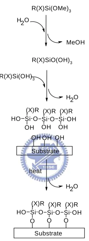
The black matrices were coated with a monolayer and the surface became hydrophobic and the surface energy was changed due to the monolayer chemicals. The monolayer chemical contains the chemical compound of fluorine as shown. Chemical 1: R(X)SiOMe3
Where R is alkyl containing fluorides X is spacer with the alkyl group
Fig. 2.1 shows the monolayer chemical formed on the substrate. The process includes coating chemical on substrate and baking. After monolayer chemical is formed, the surface of substrate will show a hydrophobic property because of the R alkyl containing fluorides. A simple process is provided to form a hydrophobic surface for preventing color ink overflowing.
R(X)Si(OMe)
3H
2
O
MeOH
R(X)SiO(OH)
3R(X)Si(OH)
3H O
2
Si O
O
H
OH
Si
OH
(X)R
O
(X)R
Si
(X)R
OH
OH
OH OH OH
Substrate
H O
2
heat
Si O
O
H
O
Si
O
(X)R
O
(X)R
Si
(X)R
O
OH
Substrate
Fig. 2.1 Monolayer chemical formed on the substrate
2.3 Plasma surface treatment
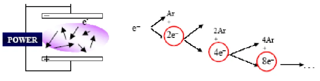
Plasma treatment is a common surface treatment to form a hydrophobic or hydrophilic surface. Different plasma has different effect. Plasma is named by Irvin Langmuir in 1929; and plasma is partial ionized gases which can be define as a quasi-neutral gas of charged &
neutral particles characterized by a collective behavior. Fig. 2.2 shows the principle of plasma
generation using Ar as an example.
Fig. 2.2 Principle of plasma generation using Ar as an example
The Kinetic Energy is the energy for plasma generation as shown in 2.2.1. (Kinetic Energy) gained = F.d = q.ε.λ = q.(V/de).λ. (2.2.1)
where λ:mean free path ; de:electrode distance ε:electric field ; V:electrode voltage
Different plasma has different effect. CFx plasma is a common method for chemical stability, low surface energy, low refractive index, good electrical and thermal insulation applications. For the purpose to prevent color ink overflowing, here we use CFx plasma as a surface treatment to decrease surface energy and to increase contact angle.
Fig. 2.3 shows the effect of plasma in the chamber. When we treat the BM substrate, other effect would influence the results. The etching effect of CFx plasma would be an issue when we using a CFx plasma surface treatment.
Chapter 3
Experiment
3.1 Experiment design
The ink-jet printer Litrex 70 as shown in Fig. 9 is used for printing R,G,B color film.
Fig. 3.1 Litrex 70 ink-jet printer
ink storage syringe, ink supply system, controller and printing head driver for ink injection, shown in Fig.3.2. The ink droplets are injected through the orifice of printing head and dropped in the substrate. The compatibility between color photoresists and printing head should be the main bottleneck issue due to different ingredients and properties of color ink and piezoelectric material of printing head [16][19].
Fig. 3.2 Basic structure of ink jet printing system
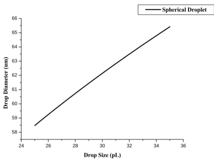
The ink-jet printing equipment is a Drop-On-Demand type printer. Print head is Spectrum piezoelectric head [17][18]. Distance between nozzle and nozzle is about 507 um and nozzle diameter is 38 um. Drops size are about 25 to 35 pl which depend on ink property and applied printing voltage. The specification of print head is shown in table 3.1. The relationship of drop size and drop diameter is shown in Fig. 3.3. Drop diameter of 25 to 35 pL droplet are about 58 to 66 um.
24 26 28 30 32 34 36 58 59 60 61 62 63 64 65 66 Dr op D iam eter (um ) Drop Size (pL) Spherical Droplet
Fig. 3.3 The relationship of drop size and drop diameter for a spherical shape drop
Table. 3.1 Specification of print head
Print Head type Spectra
SE-128
Addressable Jets 128
Drop size (pL) 25-35
Fluid viscosity range (cP) 8-20
Nozzle diameter (um) 38
3.2 Ink characterizations of IJP
For insuring the inks we used are in the specification of printing system and testing the color quality of color film, ink and color film properties are measured [28~32].
blue inks are 11.07, 7.23, and 12.99 cp. Surface tensions are 28.2, 28.0, and 28.1. The optimal viscosity for SE-128 print head is within 8 to 20 cp that the color inks are usable.
Table. 3.2 Ink and color film properties
Ink Viscosity (@ 25oC; Cp) Surface tension (@ 25oC ;mN/m) Film thickness (um) CIE1931 x y Red 11.07 28.2 1.80 0.663 0.330 Green 7.23 28.0 1.80 0.313 0.610 Blue 12.99 28.1 2.00 0.130 0.126 *Solid contain: 20 – 23 %
The optimal viscosity for SE-128 print head is within 8-20 Cp.
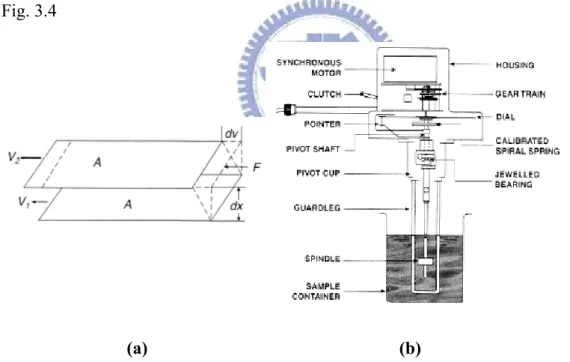
The viscosities are measured by BROOKFIELD/U.S.A DV-III+ viscosity measurement instrument. Basic theory of the viscosity measurement instrument are shown in Fig. 3.4
(a) (b)
Fig. 3.4 (a) shear for fluid by Newton (b) BROOKFIELD/U.S.A DV-III+ viscosity
measurement instrument
BROOKFIELD/U.S.A DV-III+ viscosity measurement instrument uses spindle spinning in the measured material and measures the torque when spindle is spinning as shown in Fig. 3.4(b).
in different plane has the same area of A, and the distance between the two different parallel fluid surfaces is dx. The two different parallel fluid surfaces flow in the same direction with different flowing speed. We will have an equation of:
F/A = ηdv/dx
η is viscosity and dv/dx is shear rate which means the shear of fluid. The unit of shear rate is sec-1. F/A term which called shear stress means the shearing force of fluid in per unit area. The unit of shear stress is dyne/cm2. We will have an equation of:
η = (F/A) / (dv/dx) = shear stress / shear rate The unit of viscosity is cp or mPa․s.
1 cp = 1 mPa․s
3.2.2 Color film property
Color films are formed by spin coating method. After color films are formed, they were soft baked by 90oC for 10 minutes, cured by UV light for 250 mj/cm2, and hard baked by 230oC for 40 minutes.
Fig. 3.5(a) shows the color film thickness and roughness which is measured by AFM (Atomic Force Microscope). The thickness of red, green, and blue color films are 1.81, 1.80, and 2.00 um and the roughness are 9.628, 9.294, and 8.071 nm.
Fig. 3.5(b) shows UV-visible spectrum of RGB color films of thickness shown in Fig. 3.5(a). The CIE1931 color coordinate of RGB color films are x = 0.663, y = 0330, for red color film and x = 0313, y =0610, for green color film, and x = 0.130, y =0.126, for blue color film after turning UV-visible spectrum of RGB color film to CIE1931 color coordinate [25][26].
(a)
(b)
Fig. 3.5 (a) RGB Color film thickness and roughness (b) UV-visible spectrum of RGB color
film
3.2.3 Color film reliability
The reliability of color film is used for insuring that chemical resistance of color film. Color filter is combined with other components to form a display. The reliability of color film relates to the quality of color filter.
Chemical resistance tests are using different solvent for testing as shown in Fig. 3.6. Color films are dipped into chemicals for 24 hrs.
Blue (2.00 um) 400 500 600 700 0 20 40 60 80 100 T ( % ) Wavelength (nm) R Reedd G Grreeeenn B Blluuee
Green (1.80 um) Red (1.81 um)
(a)
(b)
Fig. 3.6 UV-visible spectrum of RGB color film and CIE1931 color coordinate of chemical
1931 CIEx,y Coordinations
Red Green Blue
Original (0.580, 0.318) (0.352, 0.491) (0.161, 0.242) Methanol (0.580, 0.317) (0.351, 0.498) (0.167, 0.245) Ethanol (0.566, 0.316) (0.352, 0.470) (0.161, 0.239)
1931 CIEx,y Coordinations
Chemicals Red Green Blue NTSC
Original (0.655, 0.330) (0.300, 0.621) (0.133, 0.101) 74 % IPA (0.659, 0.330) (0.303, 0.617) (0.134, 0.108) 73 % PGMEA (0.660, 0.329) (0.310, 0.611) (0.132, 0.104) 72 % r-butyrolatane (0.664, 0.329) (0.307, 0.613) (0.133, 0.113) 72 % T ( % ) Wavelength (nm) Blank Methanol Ethanol Red Green Blue T ( % ) Wavelength (nm) IPA PGMEA r-butyrolatane
3.3 BM glass treatment
BM glass surface treatment is used for prevent ink overflow from the pixels. Here are two BM glass surface treatment process.
3.3.1 BM glass chemical treatment
Fig. 3.7 shows the chemical treatment process. A BM glass is dipped in the monolayer chemical (series No. HFC-128) and baked by 100oC for half an hour. This method will coat the chemical on both black matrices and glass. Two chemical is used in this experiment. Difference between these chemicals is the hydrophobic effect to different surface.
Fig. 3.7 Chemical treatment process
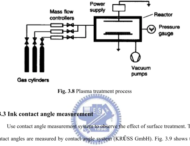
3.3.2 BM glass plasma treatment
A BM glass is put in a vacuum chamber for plasma treatment as shown in Fig. 3.8. Gas handling system is mass flow controller. Reactor includes chamber, electrode, gas distribution, gauge, and heat/cool. Pumping unit includes throttle valve, turbo-pump, and rough pump. Power supply is the source (DC, RF, and MW)/bias for plasma, and pulsed/continuous
controller. CFx gas flows into the chamber to produce CFx plasma. Control the gas flowing rate, plasma power, and treating time to have different effect of plasma treatment. This method will treat both black matrices and glass.
Fig. 3.8 Plasma treatment process
3.3.3 Ink contact angle measurement
Use contact angle measurement system to observe the effect of surface treatment. The contact angles are measured by contact angle system (KRŰSS GmbH). Fig. 3.9 shows the method of contact angle system measurement. The needle will push 3 ~ 4 uL drop at the tip and touch the substrate. After drop contact to the substrate the beadle leave the substrate and the droplet is left on the substrate.
(a) (b)
Fig. 3.9 Method of contact angle system measurement (a) wetting surface (b) not
3.4 Printing process
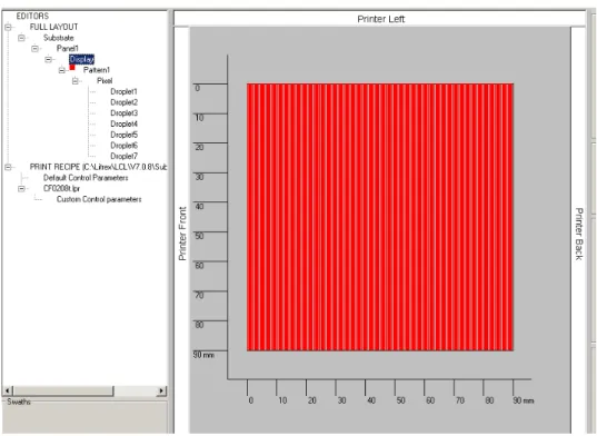
Printing design is assisted by using LSL program which is also the program used to control the Litrex 70 ink-jet printing system. Using Litrex ink-jet printing system print red, green, and blue single color films before printing three color films on same BM [21][22].
3.4.1 Printing pattern design
Red, green, and blue color films are independently printed step by step. Every printed pattern are apart from another by an applicable distance to form red, green, and blue subpixel color filter. Fig. 3.10 shows the design for one of the three primary color print pattern.
Fig. 3.10 Design for one of the three primary color print pattern using Litrex inside program
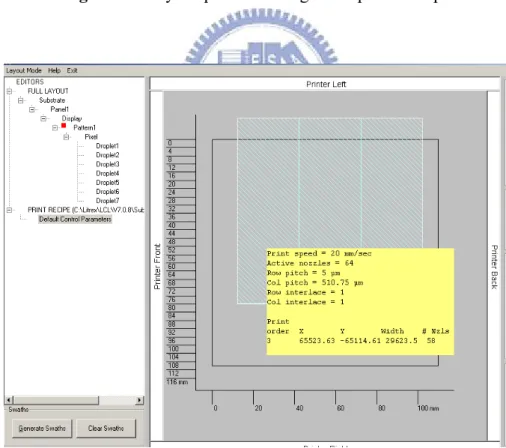
Every subpixel are designed to print 7 drops as shown in Fig. 3.11. the program will generate a mechanical langrage after completing the patter. The mechanical langrage which is called swath and the printing recipe is shown in Fig. 3.12.
Fig. 3.11 Every subpixel are designed to print 7 drops
Fig. 3.12 The mechanical langrage which is called swath and the printing recipe
[23]: Step1. Pump out the maintenance solvent out of the ink supply syringe. Step2. Inject the color ink into the ink supply syringe.
Step3. Prime the head to fill the color ink into the inside pipe and printing head. Step4. Set printing recipe and maintain the printing head to check the head
condition.
Step5. Go printing process.
Fig. 3.13 shows the drops jetting out of the nozzle taking picture by camera. Using the system, we could know the condition of nozzle and print head. Fig. 3.13(a) shows the earlier time of drops jetting out of the nozzle and Fig. 3.13(b) shows the later time.
(a) (b)
Fig. 3.13 Drops jetting out of the nozzle (a) earlier time of drops jetting out of the nozzle (b)
Chapter 4
Result & Discussion
4.1 Contact angle of BM glass surface treatment
Contact angle of droplet on substrate relates to the wetting situation between ink and substrate surface. High contact angle means the ink would not be so wetting on the surface. In order to prevent ink from overflowing the bank when printing, two surface treatments is used to increase the contact angle of droplet on BM substrate as shown in chapter 2.
Use water as a reference to show the contact angle changed after surface treatment. Fig. 4.1 shows the water on the blank BM, and the contact angle is 65o.
Fig. 4.1 Contact angle of water on blank BM
The contact angle increases from 65o to more than 85 o after surface treatment for BM side as shown in Fig 4.2. The chemical treatment is more effective than plasma treatment as shown in Fig 4.2
W
Wa
at
te
er
r
o
on
n
b
bl
la
an
nk
k
B
BM
M
C
Fig. 4.2 Contact angle of water on different treatment BM and glass
4.1.1 Contact angle of BM glass chemical surface treatment
Use chemical surface treatment to increase contact angle of color ink droplet. Fig. 4.3 shows the contact angle of red ink drop on blank BM and glass
(a) (b)
Fig. 4.3 Contact angle of red ink drop on blank BM and glass (a) blank BM (b)blank glass
Fig. 4.4 shows the contact angles of red ink drops on chemical treatment BM and glass. Contact angles increase after BM and glass chemical treatment as shown in Fig. 4.3 and Fig. 4.4. The contact angle increases obviously for red ink in chemical 1 treatment case. In order to prevent overflowing, chemical 1 treatment for large contact angle increasing would better than chemical 2 treatment.
C
Fig. 4.4 Contact angles of red ink drops on (a) chemical1 treated BM (b) chemical1 treated
glass(c) chemical2 treated BM (d) chemical2 treated glass
The contact angles of red ink drops on chemical treated surface are increased. The effect of surface treatment to other inks will be discussed next. Fig. 4.5 shows the contact angle of green ink drop on blank BM and glass.
(a) (b)
Fig. 4.5 Contact angle of green ink drop on blank BM and glass (a) blank BM (b)blank
glass
Fig. 4.6 shows the contact angles of green ink drops on chemical treatment BM and glass. Contact angles increase after BM and glass chemical treatment as shown in Fig. 4.5
C C//AA5522oo CC//AA4411oo C/A 30o C C//AA2244oo (a) (b) (c) (d) C C//AA1144oo CC//AA1166oo
case. In order to prevent overflowing, chemical 1 treatment for large contact angle increasing would better than chemical 2 treatment.
Fig. 4.6 Contact angles of green ink drops on (a) chemical1 treated BM (b) chemical1
treated glass(c) chemical2 treated BM (d) chemical2 treated glass
The contact angles of red ink drops on chemical treated surface are increased. The effect of surface treatment to blue inks will be discussed next. Fig. 4.7 shows the contact angle of blue ink drop on blank BM and glass.
(a) (b)
Fig. 4.7 Contact angle of blue ink drop on blank BM and glass (a) blank BM (b)blank glass
Fig. 4.8 shows the contact angles of blue ink drops on chemical treatment BM and
C C//AA5544oo C C//AA3344oo C C//AA2288oo C C//AA2299oo (a) (b) (c) (d) C C//AA77oo CC//AA1166oo
glass. Contact angles increase after BM and glass chemical treatment as shown in Fig. 4.7 and Fig. 4.8. The contact angle increases obviously for blue ink in chemical 1 treatment case. In order to prevent overflowing, chemical 1 treatment for large contact angle increasing would better than chemical 2 treatment.
Fig. 4.8 Contact angles of blue ink drops on (a) chemical1 treated BM (b) chemical1 treated
glass(c) chemical2 treated BM (d) chemical2 treated glass
Contact angles increase after BM and glass chemical treatment. The contact angle increases obviously in chemical 1 treatment case for red, green, and blue ink. Chemical 1 treatment for large contact angle increasing would better than chemical 2 treatment. Contact angle increases both BM and glass side after chemical treatment. In ink-jet printing color filter application, increasing contact angle of ink on BM without on glass would be a best situation to prevent overflowing but not to influence color film uniformity and color properties. C/A 39o C C//AA4400oo C C//AA3355oo C/A 32o (a) (b) (c) (d)
Use CFx plasma surface treatment to increase contact angle of color ink droplet. The power of plasma is 400w, gas flowing rate is 300 sccm, and treatment time is 5 seconds. Fig. 4.9 shows the contact angles of red ink drops on plasma treatment BM and glass. For red ink, the contact angle of plasma treatment BM side increases as shown in Fig. 4.3 and Fig. 4.9. Plasma treatment is not so effective to glass side that contact angle of glass side is not increasing obviously.
(a) (b)
Fig. 4.9 Red ink drops on CFx plasma treatment (a) BM side (b) and glass side.
Fig. 4.10 shows the contact angles of green ink drops on plasma treatment BM and glass. For green ink, the contact angle of plasma treatment BM side increases as shown in Fig. 4.5 and Fig. 4.10. Plasma treatment is not so effective to glass side that contact angle of glass side is not increasing obviously.
(a) (b)
Fig. 4.10 Green ink drops on plasma treatment (a) BM side (b) and glass side.
Fig. 4.11 shows the contact angles of blue ink drops on plasma treatment BM and
C
C//AA2277oo CC//AA1155oo
C
glass. For blue ink, the contact angle of plasma treatment BM side increases as shown in Fig. 4.7 and Fig. 4.11. Plasma treatment is not so effective to glass side that contact angle of glass side is not increasing obviously.
(a) (b)
Fig. 4.11 Blue ink drops on plasma treatment (a) BM side (b) and glass side.
Table. 4.1 Contact angle of color inks on BM and glass
without
treatment
Chemical I Chemical II CFx Plasma
BM (o) Red 12 52 24 27 Green 14 54 28 30 Blue 7 39 35 25 Water 65 105 103 85 Glass (o) Red 17 41 30 15 Green 16 34 29 15 Blue 16 40 32 15 Water 100 98 12
Contact angles increase after plasma treatment for BM side. Contrast to chemical treatment, plasma treatment is not so effective for BM. Different treatment time will cause different hydrophobic effect.
C
side effect of over etching was inevitable. To obtain an optimized condition, the plasma treatment was done experimentally between 10 to 50 seconds. Fig. 12 shows that the height of BM decreases with the treatment time increasing.
Fig. 4.12 Height of BM with the treatment time increasing from 0 to 50 seconds.
Height of BM decreases to 80% with treatment time increasing to 30 seconds. To prevent further damage on BM while keeping good hydrophobic condition, CF4 plasma
treatment time should be limited within 30 seconds.
Fig. 4.13 shows the contact angles of red ink drops on plasma treatment BM and glass by different time. The contact angle increases with treatment time increasing. Plasma treatment is not so effective to glass side that contact angle of glass side is not increasing obviously even increasing treatment time.
Fig. 4.13 Contact angles of red ink drops on different time plasma treatment BM (a1) 10s
(b1) 20s (c1) 30s and glass (a2) 10s (b2) 20s (c2) 30s.
4.1.3 Discussion of surface energy
The adhesion energy, Wa, is the energy dissociating from the original surface of two different kinds of material (for area 1cm2) and forming a new surface. Wc is the cohesion energy R.
Wa=γS+γL-γLS, Wc(L)=2γL
γS and γL are surface tensions of solid and liquid respectively. γLS is the interfacial tension
between solid and liquid. From Young’s equation:
γLcosθ=γS-γSL
where θ is contact angle. Rewrite Young’s equation and adhesion energy: Wa=γL(1+cosθ) C C//AA3300oo C C//AA1155oo C C//AA3322..55oo C/A 18o C C//AA3355oo C C//AA1199oo (a2) (b2) (c2) (a1) (b1) (c1)
As a result, the surface energy depends on the surface tension and contact angle. The contact angle was greatly increased after chemical or plasma treatment, therefore, the surface energy was greatly reduced.
4.2 Printed R G B single color film
Using Litrex ink-jet printing system print red, green, and blue single color films before printing three color films on same BM.
Use dip coating for BM glass as a chemical surface treatment. Fig. 4.14 shows the drop on dip coating surface treatment BM glass. The color ink is not wetting to form color film after dip coating chemical surface treatment. Chemical treatment by dip coating is not suitable in ink-jet printing color filter process. For this reason the printed BM is without any treatment in next sessions.
4.2.1 Printed Red single color film
Fig. 4.15 shows the printed red color film observed under POM (polarization optical microscope). There are 7 drops jetting into the bank. The profile of red color film is shown in Fig. 4.16. Thickness of color film is about 0.18 um
Fig. 4.15 The printed red color film observed under POM
0 100 200 300 400 500 600 -0.2 0.0 0.2 0.4 0.6 0.8 1.0 1.2 1.4 1.6 1.8 2.0 Hei ght (u m)
Scan length (um)
Red Ink
Fig. 4.16 The profile of red color film and the thickness of color film are about 0.18 um
measuring by α-step
300 350 400 450 500 550 600 650 700 750 75 80 85 90 95 100 105 110 Tr an sm it ta nc e wave length Red
Fig. 4.17 UV-visible spectrum of single red color film for film thickness 0.18 um
In order to increase the thickness of color film, printing process is repeated for many times. Every time jetting 6 drops into the bank for 2 um thickness color film. Fig. 18 shows different printing times of color film thickness
(a) (b)
In Fig. 18, the color film is formed as a mountain shape not to be a flat film we want. The drops are not wetting on the color film printed antecedently because the solvent on drops will be absorbed by antecedently printed color film. Drops would not flow and wetted on antecedently printed color film and a mountain-like color film is formed.
4.2.2 Printed Green single color film
Fig. 4.19 shows the printed green color film observed under POM (polarization optical microscope). There are 7 drops jetting into the bank. The profile of green color film is shown in Fig. 4.20. Thickness of color film is about 0.1 um
0 100 200 300 400 500 600 -0.2 0.0 0.2 0.4 0.6 0.8 1.0 1.2 1.4 1.6 1.8 2.0 Hei ght (u m)
Scan length (um)
Green ink
Fig. 4.20 The profile of green color film and the thickness of color film are about 0.1 um
measuring by α-step
Fig. 4.21 shows the UV-visible spectrum of single red color film.
300 350 400 450 500 550 600 650 700 750 75 80 85 90 95 100 105 110 T ransm ittance wave length Green
4.2.3 Printed Blue single color film
Fig. 4.22 shows the printed blue color film observed under POM (polarization optical microscope). There are 7 drops jetting into the bank. The profile of blue color film is shown in Fig. 4.23. Thickness of color film is about 0.2 um
Fig. 4.22 The printed blue color film observed under POM
1400 1500 1600 1700 1800 1900 2000 2100 -0.2 0.0 0.2 0.4 0.6 0.8 1.0 1.2 1.4 1.6 1.8 Hei ght ( um)
Scan length (um)
Blue ink
Fig. 4.23 The profile of blue color film and the thickness of color film are about 0.2 um
300 350 400 450 500 550 600 650 700 750 65 70 75 80 85 90 95 100 105 T ran sm ittance wave length Blue
Fig. 4.24 UV-visible spectrum of single blue color film for film thickness 0.2 um
4.3 Printed R G B color film
In session 4.2, red, green, and blue color films are printer on the BM. Printing process of RGB color film is printing red, green, and blue color film on the same BM step by step. No color mixing in printing process. Fig. 4.25 shows the RGB color filter observed under POM. Different times of printing process repeat for red, green, and blue color film. Red, green, and blue color films are printed by repeating 1, 4, and 5 times of printing process and every printing process jets 6 droplets into the bank.
Fig. 26 shows the profile of RGB color films. The thickness of red, green, and blue color films are 0.18, 0.76, and 1.0 (average) um. The color uniformity of blue is bad because of mountain-like shape of blue color film.
Fig. 4.26 The profile of RGB color films
4.4 Summery
Using Litrex 70L, we can print color films on BM accurately. Color films of red, green, and blue are single printed and printed together on BM. To prevent color ink overflowing, using surface treatment would be a method.
The contact angle is increased after chemical and CFx plasma treatment. Using chemical 1 surface treatment, the contact angles of color inks increase from about 15o to about 50o on BM side and from about 15o to 40o on glass side. Effect of chemical 2 surface
0 200 400 600 800 1000 1200 1400 1600 0.0 0.2 0.4 0.6 0.8 1.0 1.2 1.4 1.6 1.8 2.0 He ig ht ( um)
Scan length (um)
RGB ink
R R G
increase from about 15o to about 30o both on BM and glass side. The chemical treatment is efficiency to both BM side and glass side. Chemical treatment for ink-jet color filter applications could not use dip coating method. The color ink is not wetting to form color film after dip coating chemical surface treatment. Using plasma surface treatment, the contact angles of color inks increase from about 15o to about 30o on BM side but plasma surface treatment seems not so efficiency to glass side that contact angle do not increase. Increasing the plasma treatment time would increase the contact angles of color inks but also destroy the BM. After plasma treatment for 30 seconds, the height of BM decreases to 80%.
Chapter 5
Conclusion & Future work
5.1 Conclusions
Generally speaking, there is an issue for color filter printing process that color ink overflows when printing. To solve this problem, many methods of preventing ink overflowing are published and used for ink-jet printing color filter process. Here, we use surface treatment as a method to block ink overflowing and the surface treatment uses only one step process.
Use chemical coating and plasma surface treating as two kinds of surface treatment for hydrophobic treatment. Color ink would not be wetting on hydrophobic treatment thus the color ink would be blocked in subpixels without overflowing when printing.
The contact angle is increased after chemical and CFx plasma treatment. Using chemical 1 surface treatment, the contact angles of color inks increase from about 15o to about 50o on BM side and from about 15o to 40o on glass side. Effect of chemical 2 surface treatment is lower than chemical 1 surface treatment that the contact angles of color inks increase from about 15o to about 30o both on BM and glass side. The chemical treatment is efficiency to both BM side and glass side. Using plasma surface treatment, the contact angles of color inks increase from about 15o to about 30o on BM side but plasma surface treatment seems not so efficiency to glass side that contact angle do not increase. Increasing the plasma treatment time would increase the contact angles of color inks but also destroy
5.2 Future work
The color films are not flat as shown in Fig. 4.26. The color ink drops are not wetting on the color film which has been previously printed in the bank. Adjust the ink formula to solve this problem would be the next step.
Fig. 5.1 shows the ink printing on the chemical coating BM. The drop is not wetting in the bank and the color film is not formed. Dip coating process for BM is not so suitable for ink-jet printing color filter process. Use ink-jet printing process to print the chemical solution only on the BM wall, and the color ink would be wetting in the bank and blocked in subpixel without overflowing.
Reference
[1] Horng-Show K., Po-Chuan P., and T. Kawai, Appl. Phys. Lett., 88, 111908 (2006)
[2] Jee-Hong Kim, Jan P. Allebach, IEEE Transactions on Consumer Electronics, 42, 4A (1996)
[3] Chi-Jung C., Feng-Mei W., Shinn-Jen C. and Mei-Wen H., Jpn. J. Appl. Phys., 43, 6280 (2004)
[4] Duncan J. A., Proc. SPIE, 4657, 46 (2002)
[5] Chi-Jung C., Shinn-Jen C., Kuo-Chen S., Fu-Lung P., Journal of Polymer Science: Part B:
Polymer Physics, 43, 3337 (2005)
[6] Po-Chuan P., Mi C., Horng-Show K., Feng-Mei W., and Shinn-Jen C., IEICE TRANS.
ELECTRON, E89–C, 1727,(2006)
[7] Gu X., Jonathan M., Curtis P., Lone R., and Gary B., Proc. SPIE, 4669, 377 (2002) [8] Chi-Jung C., Shinn-Jen C., Feng-Mei W., Mei-Wen H., Wanda W.W. CHIU2 and Kevin
C., Jpn. J. Appl. Phys., 43, 8227 (2004)
[9] Berend-Jan de G. and Ulrich S. S., Langmuir, 20, 7789 (2004)
[10] E. Bassous, H. H. Taub and L. Kuhn, Appl. Phys. Lett., 31, 135 (1977)
[11] Yuzo I., Shinji K., Yoshimitsu A. and Yashuhiro A., Jpn. J. Appl. Phys., 39, 1490 (2000)
[12] Masamichi M., Tomoyuki K., Hideyuki O. and Atsushi Takahara, Langmuir, 21, 911 (2005)
[14] D. V. Nicolua, T. Taguchi, H. Taniguchi, S. Yoshikawa, Colloids and Surface A, 155, 51 (1999)
[15] N. Jnagaki, S. Tasaka, T. Umehara, J. Appl. Poly. Sci.,.71, 2191 (1999)
[16] Noda K., Miura M., Sugimitsu M., National Technical Report (Matsushita Electric
Industry Company), 22, 543 (1976)
[17] Heinzl J., Hertz, C. H., Advances in Electronics and Electron Physics, 65, 91 (1985) [18] L. Dong Heon, Derby B., Journal of the European Ceramic Society, 24, 1069 (2004) [19] S. Xiao-Hong, Z. Tian-Wen, G. Mao-Zu, Wang. Ya-Dong, Journal of Harbin Institute
of Technology, 9, 270 (2002)
[20] P. Alfred I.-Tsung, Proc. SPIE, 3422, 38 (1998)
[21] Zhao X., Evans, J.R.G., Edirisinghe, M.J., Song J.H., Ceramics International, 29, 887 (2003)
[22] A. Heather, A. David M. Proc. SPIE, 4019, 446 (2000)
[23] Stephany, Timothy J., Journal of Microelectromechanical Systems, 16, 351 (2007) [24] S. Dae Ho, C. Min Hee, K. June Young, J. Jin, Kirchmeyer S., Appl. Phys. Lett., 90,
053504 (2007)
[25] L. Rastislav, S. Bogdan, P. Konstantinos N., Venetsanopoulos, Anastasios N., Proc.
SPIE, 5150 III, 1642 (2003)
[26] K. Takashi, S. Takahiro, Proc. SPIE, 5301, 334 (2004)
[27] Z. Baolong, K. Hoi-Sing, H. Ho-Chi, Journal of Applied Physics, 98, 123103 (2005) [28] S. Ram W., Displays, 20, 119 (1999)
[29] L. Baozhong, H. Tianbai, D. Mengxian, S. Xibin, H. Ximin, Thin Solid Films, 303, 213 (1997)
[30] Ishikawa T., Miyai H., Yamazaki T., Seid H., Kusunose H., Yoshimoto H.,
IDW/AD'05, 1 ,335 (2005)
Papers - SID International Symposium, 36, 880 (2005)
[32] Koo H.S., Liu Y.T., Cho L.P., Chang S.J., Wu F.M., Goang D.Y., IDMC'05, p 627-628 (2005)