行政院國家科學委員會專題研究計畫 成果報告
前瞻性可程式化正交頻分調變(OFDM)數位訊號處理核心技
術之研究
計畫類別: 個別型計畫 計畫編號: NSC92-2213-E-009-109- 執行期間: 92 年 08 月 01 日至 93 年 07 月 31 日 執行單位: 國立交通大學電信工程學系 計畫主持人: 紀翔峰 計畫參與人員: 王來輝,謝青洋,林敬傑 報告類型: 精簡報告 報告附件: 出席國際會議研究心得報告及發表論文 處理方式: 本計畫可公開查詢中 華 民 國 93 年 11 月 16 日
行政院國家科學委員會專題研究計畫成果報告
用於正交頻分調變(OFDM)之可程式化數位訊號處理核心
Programmable Radio Processing Engine Core Architecture for OFDM
Transceivers
計畫編號:NSC 92-2213-E-009-109
執行期限:92 年 08 月 01 日至 93 年 07 月 31 日
主持人:紀翔峰助理教授 國立交通大學電信工程學系
計畫參與人員: 王來輝 謝青洋 林敬傑 國立交通大學電信工程學系
Abstract
This goal of this project is to design a low-cost OFDM-specific programmable radio processor architecture, which is aimed to provide a cost-effective high-performance hardware solution for OFDM-base SDR.
Different from other OFDM radio processors, which are huge and designed to cover high-complexity processing functions like FFT/IFFT and Viterbi decoder, our processor is dedicated for heterogeneous functions of multi-mode systems. This RISC-type processor is small and low-cost so that no redundant hardware cost will be consumed. This report describes the micro-architecture and the instruction sets of this radio processor core.
1. INTRODUCTION
In recent years, OFDM (Orthogonal Frequency Division Multiplexing) technology causes much attention because of the ability of solving the multiple-path problem in wireless communications. In OFDM, many operations, such as packet detection, timing recovery, and channel estimation, are done in the frequency domain. The computation of complex numbers will be needed frequently. Under this consideration, we design a radio processor which has the ability to perform complex-number computation. Besides, in a wireless system, because the channel environment changes from time to time, we have to use different modulation to get better performance. To accomplish the adaptive modulation schemes in an efficient way, the radio processor approach can be adopted because of the flexibility and the programmability. The subject of this project is to design a small but efficient programmable radio processor for OFDM systems.
In our programmable radio processor, two modes are used. One is complex mode and the other is real mode. In complex mode, the processor offers a complex instruction set, which is dedicated for complex-number computation. For example, it can finish one complex multiplication and accumulation in one cycle whereas the same operation may need four cycles for the general-purpose DSP. In addition, it contains many instructions which facilitate computation of complex numbers. In real mode, another instruction set is design for real-number computation. We use the architecture like SIMD (Single Instruction, Multiple Data) architecture in real mode to process multiple data in one cycle. For example, it can complete four real multiplications and accumulations in one cycle with the instruction in real mode. Therefore, with using SIMD architecture the programmable radio processor can reach higher computational processing rate.
In order to increase the operation clock speed, there are four stages in the instruction pipeline of the processor. They are Fetch, Decode, Execution, and Writeback. The data hazards and the control hazards have been carefully analyzed, and the timing penalty will be presented in this report.
2. COMPLEX–MODE ARCHITECTURE
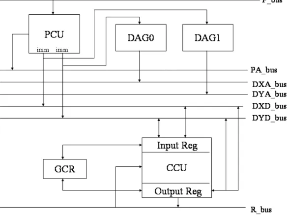
Figure 1 shows the complex-mode architecture of the radio processor. It contains components as following list:
Buses
Complex computational unit (CCU) Program control unit (PCU)
Data address generator (DAG) 0&1 General complex registers (GCR)
Each component of the complex-mode architecture will be described in detail in the following statements.
Figure 1. Complex-mode Architecture
Buses
The processor has two complex data memory blocks: CDMX and CDMY, so there are two buses about data memories. There are seven buses in the complex-mode architecture:
P_bus: program memory bus
PA_bus: program memory address bus DXA_bus: data memory (X) address bus DYA_bus: data memory (Y) address bus DXD_bus: data memory (X) data bus DYD_bus: data memory (Y) data bus R_bus: Result bus
Complex computational unit (CCU)
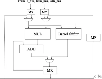
The complex computational unit (CCU) provides complex computations and has partial functions of an ALU, a MAC and a shifter. It can perform complex computations such as multiplication, multiplication with cumulative addition, multiplication with cumulative subtraction, addition, subtraction, shifting, squaring, etc. The CCU structure is showed in figure 2.
Figure 2. CCU block diagram
There are four complex registers in the CCU structure. MCX and MCY are the complex source registers, and they can be written from DXD bus and DYD bus. MCF is the complex feedback register which allows the result to be used directly as one input of the multiplier. MCR is the complex result register which contains the computational result. Moreover, MCR can be used as the other input of the multiplier with the help of R bus.
Program control unit (PCU)
The program control unit (PCU) controls the flow of program execution. It reads data from instruction memory and generates an instruction address. PCU allows sequential instruction execution, looping operation, branches, and calls and also can provide immediate data to computational unit.
Data address generator (DAG) 0&1
memory, X and Y, so that two data memory can be accessed simultaneously. The DAG contains three register files: the modify (M) register file, the index (I) register file, and the length (L) register file. The index registers contain the actual addresses used to access memory. There are four index registers, I0~I3, in DAG0 and another four index registers, I4~I7, in DAG1. The modified register is added to the specified index register to generate the updated index value. M0~M3 are in DAG0 and M4~M7 are in DAG1. The length registers (L) are used to set circular buffer size. If L is set to zero, a linear buffer is used; if L is non-zero value, a circular buffer with size L is used to produce corresponding addresses.
General complex registers (GCRs)
For many operations, there are sometimes intermediate values of computations that need to be saved temporarily. For this purpose, the radio processor contains four complex registers, GCR0~GCR3, to do such job and these four registers are general complex registers (GCRs). They can save the intermediate data which are produced by the computational unit, and can offer the intermediate data which computational unit wants.
3. REAL-MODE ARCHITECTURE
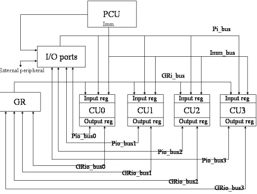
Figure 3 shows the architecture of the radio processor in real mode. There are several components in the real-mode architecture as following list:
Buses
Computational units (CU) 0, 1, 2, 3 Program control unit (PCU)
Input and output (I/O) ports General registers (GR)
Each component of the complex-mode architecture will be described in detail in the following statements.
Figure 3. Real-mode Architecture
Buses
There are several internal buses in the real-mode architecture of the processor:
Pi_bus: the bus is used to transmit data from I/O ports to input registers of computational units.
Imm_bus: the bus is used to transmit immediate data from program control unit to input registers of computational units.
Gri_bus: the bus is used to load data from general register files to input registers of computational units.
Pio_bus0~3: I/O ports can be loaded and stored data from the output registers of computational units (CU0~3) with using the corresponding Pio_bus (Pio_bus0 is corresponding to CU0, etc.). The output registers of CUs can also be loaded and
stored data from I/O ports with using the corresponding Pio_bus.
Grio_bus0~3: as Pio_buses for transmit data between I/O ports and the output registers of Cus, Grio_buses allow data transmission between general register files and the output registers of CUs.
Computational units (CU) 0, 1, 2, 3
In the real-mode architecture, four computational units (CUs) offer high processing rate computation. The four CUs have the same structure which can perform addition, subtraction, multiplication, division, multiplication with cumulative addition, multiplication with cumulative subtraction, shifting, and other arithmetic computation. Figure 4 shows the CU’s structure. There are four registers in a CU : MX, MY, MR, MF. MX and MY are the source registers, MR is the result register, and MF is the feedback register. The inputs of CUs can be writed by three sources: the immediate data from PCU (Imm_bus), the external data from I/O ports (Pi_bus), and intermediate data from GRs (GRi_bus). The ouputs of CUs can be loaded and stored by two sources, one is I/O ports and the other is GRs.
The four CUs can perform multiple computations in one cycle so the processor in real mode has the architecture which is like that of SIMD and therefore the processor can offer high processing rate computation in real mode.
Figure 4. CU block diagram
Program control unit (PCU)
The PCU in real mode has the same function of that in complex mode. It controls the program flow, generates the instruction address, and transmits immediate data to CUs. In addition, PCU will also send control signal to I/O ports to inform which port is to be loaded or stored.
Input and output (I/O) ports
The radio processor provides eight I/O ports in the real-mode architecture. The I/O ports are the medium between the processor and external peripherals. When the processor read/write a data from/to an I/O port, it will send a signal to inform the external peripheral that the state of the I/O ports has been changed. Therefore, there must be certain responses to the update of the I/O ports for certain applications.
General registers (GR)
In complex-mode architecture, the processor has four general complex registers (GCRs). A complex register is composed of two real registers, so these four GCRs become eight general registers (GRs) in real-mode architecture. The purpose of GR is to store the intermediate data from computations, so it can be read and written by CUs with the GRio buses and can load data to CU with the GRi buses.
4. INSTRUCTION SET
Complex Mode
Class 1: Addition : R = X+Y Subtraction : R = X-Y R : MCR, MCF X : MCX, MCR Y : MCY, MCF Class 2: Multiplication : R = X*YMultiplication with accumulative addition: R = MCR + X*Y Multiplication with accumulative subtraction: R = MCR - X*Y R : MCR, MCF
X : MCX, MCR Y : MCY, MCF
Class 3:
Square : R = X2
Square with accumulative addition: R = MCR + X2 Square with accumulative subtraction: R = MCR - X2
R : MCR, MCF X : MCX, MCR, MCY, MCF Class 4: Conjugate : R = conj(X) Negate : R = -X R : MCR, MCF X : MCX, MCR, MCY, MCF Class 5:
Right shift : R = X >> Imm. Left shift : R= X << Imm. R : MCR, MCF
X : MCX, MCR, MCY, MCF
The immediate value of shift is allowed to be 0~255.
Class 6:
Indirect data memory load : R = CDMn(Ix) Indirect data memory store : CDMn(Ix) = R R : MCX, MCR, MCY, MCF
n is to choose one of the two complex data memories(CDM). If n is zero then choose CDM0; otherwise, choose CDM1. x is to choose the index register of the DAG.
For CDM0, x can be 0~3; for CDM1, x can be 4~7.
Class 7:
Immediate data memory load : R = CDMn (Imm) Immediate data memory store : CDMn (Imm) = R R : MCX, MCR, MCY, MCF
n : 0, 1 (choose CDM0 or CDM1)
The immediate value can be 0~255. If the immediate value is larger than 255, one extra instruction will be used to carry the immediate data. In other words, if immediate value is lager than 255, two instructions will be needed to do the job of memory accesses. With the extra instruction, the field of immediate data can reach up to 24 bits.
Class 8:
Register move : regD = regS
regD : MCX, MCR, MCY, MCF, GCR0~GCR3 regS : MCX, MCR, MCY, MCF, GCR0~GCR3
Class 9:
Load real immediate data : reg = ImmRe Load imaginary immediate data : reg = ImmIm
Load complex immediate data : reg = ImmCR, ImmCI reg: MCX, MCR, MCY, MCF
ImmRe: 0~255, real immediate data ImmIm:0~255, imaginary immediate data ImmCR: 0~15, real part of a complex number ImmCI:0~15, imaginary part of a complex number
If the immediate data excesses the corresponding range, one extra instruction will be used and can has another 16-bit field for it.
Class 10.
Addition with two memory read : R = X+Y, X = CDMnx(Ix), Y=CDMny(Iy) Subtraction with two memory read : R = X-Y, X = CDMnx(Ix), Y=CDMny(Iy) R : MCR, MCF
X : MCX, MCR Y : MCY, MCF
nx. ny : 0, 1 (choose CDM0 or CDM1) Ix.Iy : 0~3 for CDM0, 4~7 for CDM1
The instruction allows user to load data after addition or subtraction in the same cycle.
Class 11:
Multiplication with two memory read :
R = X*Y, X = CDMnx(Ix), Y=CDMny(Iy) Multiplication / accumulative addition with two memory read :
R = MCR + X*Y, X = CDMnx(Ix), Y=CDMny(Iy) Multiplication / accumulative subtraction with two memory read :
R = MCR - X*Y, X = CDMnx(Ix), Y=CDMny(Iy) R : MCR, MCF
X : MCX, MCR Y : MCY, MCF
nx.ny : 0, 1 (choose CDM0 or CDM1) Ix.Iy : 0~3 for CDM0, 4~7 for CDM1
The instruction allows user to load data after multiplication or MAC computations in the same cycle.
Class 12:
Square with memory read :
Square / accumulative addition with memory read :
R = MCR + X2 , X = CDMn(Ix) Square / accumulative subtraction with memory read :
R = MCR - X2 , X = CDMn(Ix) R : MCR, MCF
X : MCX, MCR, MCY, MCF n : 0, 1 (choose CDM0 or CDM1) Ix.Iy : 0~3 for CDM0, 4~7 for CDM1
The instruction allows user to load data after square or square/ accumulative addition and accumulative subtraction computations in the same cycle.
Class 13:
Addition with single memory read : R = X+Y, Z = CDMn(Ix) Subtraction with single memory read : R = X-Y, Z = CDMn(Ix) R : MCR, MCF X : MCX, MCR Y : MCY, MCF Z : X, Y nx : 0, 1 (choose CDM0 or CDM1) Ix : 0~3 for CDM0, 4~7 for CDM1 Class 14:
Multiplication with single memory read :
R = X*Y, Z = CDMn(Ix) Multiplication / accumulative addition with single memory read :
R = MCR + X*Y, Z = CDMn(Ix) Multiplication / accumulative subtraction with single memory read : R = MCR - X*Y, Z = CDMn(Ix) R : MCR, MCF X : MCX, MCR Y : MCY, MCF Z : X, Y nx : 0, 1 (choose CDM0 or CDM1) Ix : 0~3 for CDM0, 4~7 for CDM1 Class 15:
Load immediate data to index registers of DAGs : In = Imm Load immediate data to modify registers of DAGs : Mn = Imm n : 0~7
registers.
If the immediate value is out of the range, one extra instruction must be used to increase 16-bit field for immediate data.
Class 16:
Load immediate data to loop counter register (LCR) : LCR = Imm
The loop counter register (LCR) is used when a DO-WHILE loop is operated. If LCR equals zero, it will enter into the loop; else, the DO-WHILE loop is end.
The range of the immediate value is 0~255, and if the immediate value is out of the range, one extra instruction must be used to increase 16-bit field for immediate data.
Class 17:
Call functions : Call <imm. addr.>
Call and push registers into stack : CallPR <imm. addr.>
The <imm. addr.> represent a relative address from present program count and is range from -127~128.
If the immediate value is out of the range, one extra instruction must be used to increase 16-bit field for immediate data.
Class 18:
Conditional jump : jump(cond.) <imm. addr.> Jump if condition is true.
The condition is as following list : • I > 0 • I <= 0 • I = 0 • I ≠ 0 • I < 0 • I >= 0 • I ov. • I not ov. • R > 0 • R <= 0 • R = 0 • R ≠ 0 • R < 0 • R >= 0 • R ov. • R not ov. • C = 0 • C ≠ 0 • C ov. • C not ov. • Counter • always where
I : the imaginary part of the computational result R : the real part of the computational result
C : the complex number of the computational result ov : overflow of computational result
counter : jump if LCR is not zero always : always jump
Class 19:
Return from subroutine : RTS Return from interrupt : RTI Sleep : SLEEP
No operation : NOP
Real Mode
Class 1:Addition : R0 = X0+Y0, R1 = X1+Y1, R2 = X2+Y2, R3 = X3+Y3 Subtraction : R0 = X0-Y0, R1 = X1-Y1, R2 = X2-Y2, R3 = X3-Y3 R : MR, MF
X : MX, MR Y : MY, MF
The number after R, X and Y is corresponding to the CU. For example, R0, X0 and Y0 is corresponding to CU0; R1, X1 and Y1 is corresponding to CU1, etc.
In real mode, the processor allows users to perform up to four additions or subtraction in one cycle by programmer’s requirement.
Class 2:
Multiplication : R0 = X0*Y0, R1 = X1*Y1, R2 = X2*Y2, R3 = X3*Y3 Multiplication with accumulative addition :
R0 = MCR0 + X0*Y0, R1 = MCR1 + X1*Y1, R2 = MCR2 + X2*Y2, R3 = MCR3 + X3*Y3
Multiplication with accumulative subtraction :
R0 = MCR0 - X0*Y0, R1 = MCR1 - X1*Y1, R2 = MCR2 - X2*Y2, R3 = MCR3 - X3*Y3
R : MR, MF X : MX, MR Y : MY, MF
Like instructions in class 1, programmer can perform up to four multiplications and multiplications/accumulations in one cycle by their requirement.
Class 3:
Square : R0 = X02, R1 = X12, R2 = X22, R3 = X32 Square with accumulative addition :
R0 = MR0+X02, R1 = MR1+X12, R2 = MR2+X22, R3 = MR3+X32 Square with accumulative subtraction :
R0 = MR0-X02, R1 = MR1-X12, R2 = MR2-X22, R3 = MR3-X32 R : MR, MF
X : MX, MR, MY, MF
Like instructions in class 1, programmer can perform up to four squares and squares/accumulations in one cycle by their requirement.
Class 4:
Absolute : R0 = abs(X0), R1 = abs(X1), R2 = abs(X2), R3 = abs(X3) Negate : R0 = -X0, R1 = -X1, R2 = -X2, R3 = -X3
R : MR, MF
X : MX, MR, MY, MF
Like instructions in class 1, programmer can perform up to four squares and squares/accumulations in one cycle by their requirement.
Class 5:
Step divide : R0 /= X0, R1 /= X1, R2 /= X2, R3 /= X3
Add if R less than zero : R0 *= R0+X0, R1 *= R1+X1, R2 *= R2+X2, R3 *= R3+X3 R : MR, MF
X : MX, MR, MY, MF
Like instructions in class 1, programmer can perform up to four squares and squares/accumulations in one cycle by their requirement.
The instructions in class 5 are used for division arithmetic.
Because there is no divider in the processor (hardware cost issue), we must use another division algorithm to perform division arithmetic. The algorithm we use is non-restoring division algorithm which is introduced in Section 4.3, page 252, Digital Computer Arithmetic-design and implementation by J. Cavanagh, 1985 McGraw-Hill.
These instructions are used to form the macro of division arithmetic, so programmer can use division as the form of Q = A/B.
Class 6:
Right shift :
R0 = X0 >> Imm0, R1 = X1 >> Imm0, R2 = X2 >> Imm1, R3 = X3 >> Imm1 Left shift :
R0 = X0 << Imm0, R1 = X1 << Imm0, R2 = X2 << Imm1, R3 = X3 << Imm1 R : MR, MF
X : MX, MR, MY, MF
The immediate value of shift is allowed to be 0~15.
The processor allows programmers to perform up to four shiftings but can only use two immediate values to specify the shifting amount owing to the constraint of the instruction length.
Imm0 : shifting value for CU0 and CU1 Imm1 : shifting value for CU2 and CU3
Class 7:
Load up to four data from input ports to CUs: X = IPn1, Y = IPn2, Z = IPn3, W = IPn4 X. Y. Z. W : MX0~3, MY0~3, MF0~3, MR0~3 IP : input port
n1. n2. n3. n4 : 0~7, the serial number of input ports
For the purpose of free-style programming, the processor allows programmers to load up to eight data from input ports to the registers in CUs in one cycle. The instruction which can load 1~4 data is in this class (Class 7) and the one which can load 5~8 data is in the next class (Class 8).
Class 8:
Load 5~8 data from input ports to CUs:
X = IPn1, Y = IPn2, Z = IPn3, …, W = IPn8 X. Y. Z. W : MX0~3, MY0~3, MF0~3, MR0~3 IP : input port
n1. n2. n3. n4. n5. n6. n7. n8 : 0~7, the serial number of input ports
The instruction in Class 8 allows user to load 5~8 data from input ports to the registers of CUs.
Class 9:
Store up to four data from CUs to output ports : OPn1 = X, OPn2 = Y, OPn3 = Z, OPn4 = W X. Y. Z. W : MX0~3, MY0~3, MF0~3, MR0~3 OP : output port
n1. n2. n3. n4 : 0~7, the serial number of input ports
The processor offer users up to four store operations from the registers of CUs to output ports in one cycle.
Unlike load instructions, because there are mostly four results which are produced by the four CUs and are needed to be stored to output ports, the store instruction offers only up to four data accesses in one cycle.
Class 10:
Register move from GRs to CUs : X = GRn1, Y = GRn2, Z = GRn3, W = GRn4 Register move from CUs to GRs : GRn1 = X, GRn2 = Y, GRn3 = Z, GRn4 = W X. Y. Z. W : MX0~3, MY0~3, MF0~3, MR0~3
n1. n2. n3. n4 : 0~7, the serial number of GRs
With the instructions in Class 10, users can move up to four registers from/to GRs to /from CUs in one cycle.
Class 11:
Load one immediate data to the registers in CUs : X = Imm
Load two immediate datas to the registers in CUs : X = Imm1, Y = Imm2 X. Y : MX0~3, MY0~3, MF0~3, MR0~3
If programmer load only one immediate data, the immediate value can be in the range : -32768~32767 (16-bit field).
For loading two immediate data, the range of each immediate value is : -128~127 (8-bit field).
Class 12:
Reset : MR = 0, MF = 0
Reset the both MR registers (MR0~3) and MF registers (MF0~3) or either of them.
Class 13:
Additions with memory read : R0 = X0+Y0, X0 = IPn1, Y0 = IPn2, R1 = X1+Y1, X1 = IPn3, Y1 = IPn4, R2 = X2+Y2, X2 = IPn5, Y2 = IPn6, R3 = X3+Y3, X3 = IPn7, Y3 = IPn8 Subtractions with memory read : R0 = X0-Y0, X0 = IPn1, Y0 = IPn2,
R1 = X1-Y1, X1 = IPn3, Y1 = IPn4, R2 = X2-Y2, X2 = IPn5, Y2 = IPn6, R3 = X3-Y3, X3 = IPn7, Y3 = IPn8 R : MR, MF
X : MX, MR Y : MY, MF IP : input port
n1. n2. n3. n4. n5. n6. n7. n8 : 0~7, the serial number of input ports
Like instructions in class 1, programmer can perform up to four additions/memory access and subtractions/memory access in one cycle by their requirement.
Class 13:
Multiplication : R0 = X0*Y0, X0 = IPn1, Y0 = IPn2, R1 = X1*Y1, X1 = IPn3, Y1 = IPn4, R2 = X2*Y2, X2 = IPn5, Y2 = IPn6, R3 = X3*Y3, X3 = IPn7, Y3 = IPn8 Multiplication with accumulative addition :
R1 = MR1 + X1*Y1, X1 = IPn3, Y1 = IPn4, R2 = MR2 + X2*Y2, X2 = IPn5, Y2 = IPn6, R3 = MR3 + X3*Y3, X3 = IPn7, Y3 = IPn8 Multiplication with accumulative subtraction :
R0 = MR0 - X0*Y0, X0 = IPn1, Y0 = IPn2, R1 = MR1 - X1*Y1, X1 = IPn3, Y1 = IPn4, R2 = MR2 - X2*Y2, X2 = IPn5, Y2 = IPn6, R3 = MR3 - X3*Y3, X3 = IPn7, Y3 = IPn8 R : MR, MF
X : MX, MR Y : MY, MF IP : input port
n1. n2. n3. n4. n5. n6. n7. n8 : 0~7, the serial number of input ports
Like instructions in class 1, programmer can perform up to four multiplications/memory access and multiplications /accumulations/memory access in one cycle by their requirement.
Class 14:
Square : R0 = X02, X0 = IPn1, R1 = X12, X1 = IPn3, R2 = X22, X2 = IPn5, R3 = X32, X3 = IPn7
Square with accumulative addition : R0 = MR0 + X02, X0 = IPn1, R1 = MR1 + X12, X1 = IPn3, R2 = MR2 + X22, X2 = IPn5, R3 = MR3 + X32, X3 = IPn7
Multiplication with accumulative subtraction : R0 = MR0 - X02, X0 = IPn1, R1 = MR1 - X12, X1 = IPn3, R2 = MR2 - X22, X2 = IPn5, R3 = MR3 - X32, X3 = IPn7 R : MR, MF X : MX, MR, MY, MF IP : input port
n1. n2. n3. n4. n5. n6. n7. n8 : 0~7, the serial number of input ports
Like instructions in class 1, programmer can perform up to four squares/memory access and squares /accumulations/memory access in one cycle by their requirement.
Class 15 :
The range of the immediate value is -32768~32767 (16-bit field).
The loop counter register (LCR) is used when a DO-WHILE loop is operated. If LCR equals zero, it will enter into the loop; else, the DO-WHILE loop is end.
Class 16:
Call functions : Call <imm. addr.>
Call and push registers into stack : CallPR <imm. addr.>
The <imm. addr.> represent a relative address from present program count and has the range : -32768~32767 (16-bit field).
Class 17:
Set config register : SETCR IPX0 = n1, IPY0 = n2, IPX1 = n3, IPY1 = n4, IPX2 = n5, IPY2 = n6, IPX3 = n7, IPY3 = n8 IP : input port
n1. n2. n3. n4. n5. n6. n7.n8 : 0~7, the serial number of input ports
the instruction in Class 17 is used to set the loading ports of X0~3 and Y0~3 when using the instructions of computation with data read. Because of the constrain of instruction length, a config register is needed to specify the loading ports of the source registers.
Class 18:
Conditional jump : jump(cond.) <imm. addr.> Jump if condition is true.
The <imm. addr.> represent a relative address from present program count and has the range : -32768~32767 (16-bit field).
The condition is as following list : • R > 0 • R <= 0 • R = 0 • R ≠ 0 • R < 0 • R >= 0 • R ov. • R not ov. • Counter • always where
R : the computational result
ov : overflow of computational result counter : jump if LCR is not zero always : always jump
Class 19:
Return from subroutine : RTS Return from interrupt : RTI Sleep : SLEEP
5. INSTRUCTION PIPELINING
No operation : NOP
There are four stages in the instruction pipeline of the processor. They are Fetch, Decode, Execution, and Writeback. The program control tasks are mostly performed in Decode-stage. The computation tasks, address update tasks, register move, and memory access are done in Execution-stage. The memory read data is ready at the start of Writeback-stage so that this datum is written back to register in this stage. There are more detail about instruction pipeline in the following.
Instruction memory address and program counter
The instruction length in the complex mode is 16 bits and in the real mode is 32 bits. In order to fit both complex and real mode, the 32-bit wide instruction memory is addressed by 16 bits as Figure 5. 31 1615 0 Addr 0 Addr 1 2 3 4 5 6 7 . . . . . . . . . . . . Instruction memory
Figure. 5 instruction memory address
The program counter (PC) contains the address of the currently executing instruction and is divided into two parts. One is PC_s, which contains the lowest bit of program counter, and the other is PCP, which contains other bits of PC. In real mode, the proccessor fetches instructions with PCP. In complex mode, in addition to fetching 32-bit memory with PCP, it must select the correct 16-bit instruction. PC_s contains the lowest bit of PC so we can use it to decide lower 16 bits or higher 16 bits to be selected. For example : in real mode, if PC is 8, then PCP is 4 and it will fetch the 32-bit instruction memory at 4th slice; in complex mode, if
PC is 8, then PCP is 4 and PC_s is 0, and it will fetch the 32-bit instruction memory at 4th slice and select the higher 16-bit instruction memory.
Pipelining PC and registers
PCP : PC containing the address of instruction that will be fetching PCF : PC containing the address of instruction in Fetch-stage PCD : PC containing the address of instruction in Decode-stage PCE : PC containing the address of instruction in Execute-stage IRD : pipelining register at Fetch/Decode-stage
IRE : pipelining register at Decode/Execute-stage IRW : pipelining register at Execute/Writeback-stage
Complex Mode
Figure 6 shows the pipelining architecture in the complex mode. In the Fetch-stage, the proccessor fetches instruction by PCP from Imem (instruction memory) and the 16-bit fetching memory is selected by Ins_sel block. The function of Ins_sel block is to select 32-bit instruction memory in real mode or 16-bit instruction memory in complex mode. In complex mode, the Ins_sel also need to judge that either the upper or the lower part of 32-bit instruction memory is selected. The Ins_sel block is controlled by mode reg and PC_s. The mode reg has the information about mode status (real or complex mode), and the PC_s is used to select upper or lower part of 32-bit instruction in complex mode.
In the Decode-stage, next program counter (PC) is selected from four sources : 1. Current PC +1 (sequential instruction execution)
2. PC stack (return from a calling function) 3. IRD register (jump to a immediate address)
4. IRE register (jump to a immediate address and the condition is mv) In the Execute-stage, the following jobs are performed:
1. When performing a call-function instruction, PCD will be pushed to PC stack.
2. When performing a store instruction, data memory will be written from MCX, MCY, MCF, MCR, and mrdata (memory read data).
3. When performing a load instruction, data will be read from data memory (mrdata). 4. The address generator updates AI register.
5. Computation of arithmetic instructions is performed in this stage. 6. Registers-move is done in this stage.
In the Writeback-stage, mrdata is written to register file(MCX, MCY, MCF, MCR) when reading memory data.
Real Mode
Figure 7 shows the pipelining architecture in the real mode. In the Fetch-stage, it fetches 32-bit instruction memory and Ins_sel blcok selects all the 32-bit passed to next stage. In the Decode-stage, the jobs done is almost the same with those in complex mode. The only difference is that PC is added by two when the program flow is sequential.
In the Execute-stage, the following jobs are performed:
1. When performing a call-function instruction, PCD will be pushed to PC stack.
2. When performing a store instruction, output ports will be written from MX, MY, MF, MR, and mrdata (memory read data).
3. When performing a load instruction, data will be read from input ports (mrdata). 4. Computation of arithmetic instructions is performed in this stage.
5. Registers-move is done in this stage.
In the Writeback-stage, mrdata is written to register file(MX, MY, MF, MR) when reading input-port data.
Pipeline diagrams
1. Normal operation
Fet-n Dec-n Exe-n WB-n
PCP n n+1
Fetch n-1 n n+1
Decoder n-1 n n+1
Execution n-1 n n+1
Writeback n-1 n n+1
2. n: if(cond) JUMP m (taken) …
m: …;
Fet-n Dec-n Exe-n WB-n
PCP n n+1 m m+1 m+2 Fetch n-1 n n+1 m m+1 m+2 Decoder n-1 n n+1 m m+1 m+2 NOP_INS Execution n NOP m m+1 Writeback n NOP m
3. n: if(cond) JUMP m (taken) …
m: if(cond) JUMP k (taken)
…; Fet-n Dec-n Exe-n WB-n
PCP n n+1 m m+1 k
Fetch n-1 n n+1 m m+1 k
Decoder n-1 n n+1 m m+1 k
NOP_INS
Execution n-1 n NOP m NOP k
Writeback n-1 n NOP m NOP k
n: if(mv) JUMP m (taken) …
m: …;
Fet-n Dec-n Exe-n WB-n
PCP n n+1 n+2 m m+1 m+2
Fetch n-1 n n+1 n+2 m m+1 m+2
Decoder n-1 n n+1 n+2 m m+1 m+2
NOP_INS
Execution n-1 n NOP NOP m m+1 m+2
Writeback n-1 n NOP NOP m m+1 m+2
5. n-1: MR-MX*MY;
n: if(mv) JUMP m (taken) …
m: if(cond) JUMP k; (taken)
Fet-n Dec-n Exe-n WB-n
PCP n n+1 n+2 m m+1 k
Fetch n-1 n n+1 n+2 m m+1 k
Decoder n-1 n n+1 n+2 m m+1 k
NOP_INS
Execution n-1 n NOP NOP m NOP k
Writeback n-1 n NOP NOP m NOP k
6. n: if(all cond) JUMP m (not taken) …
m: …;
Fet-n Dec-n Exe-n WB-n
PCP n n+1 n+2 n+3 n+4
Fetch n-1 n n+1 n+2 n+3 n+4
Decoder n-1 n n+1 n+2 n+3 n+4
Execution n-1 n n+1 n+2 n+3 n+4
Writeback n-1 n n+1 n+2 n+3 n+4
… m: …;
Fet-n Dec-n Exe-n WB-n
PCP n n+1 m m+1 m+2 Fetch n-1 n n+1 m m+1 n+2 Decoder n-1 n n+1 m m+1 n+2 NOP_INS pc_stack Execution n-1 n NOP m m+1 m+2 Writeback n-1 n NOP m m+1 m+2 n+1 8. n-1: MR-MX*MY; n: if(mv) call m (taken) …
m: …;
Fet-n Dec-n Exe-n WB-n
PCP n n+1 n+2 m m+1 m+2
Fetch n-1 n n+1 n+2 m m+1 m+2
Decoder n-1 n n+1 n+2 m m+1 m+2
NOP_INS pc_stack
Execution n-1 n NOP NOP m m+1 m+2
Writeback n-1 n NOP NOP m m+1 m+2
n+1 n+1
m+1: …
n: if(cond) RTS (taken)
Fet-n Dec-n Exe-n WB-n
PCP n n+1 m+1 m+2 m+3 Fetch n-1 n n+1 m+1 m+2 n+3 Decoder n-1 n n+1 m+1 m+2 n+3 NOP_INS pc_stack Execution n-1 n NOP m+1 m+2 m+3 Writeback n-1 n NOP m+1 m+2 m+3 10. … n: cmd … …
Fet-n Dec-n Exe-n WB-n
PCP n n+1 n+1 n+1 n+2 n+3
Fetch n-1 n n+1 n+1 n+1 n+2 n+3
Decoder n-1 n n+1 n+1 n+1 n+2 n+3
NOP_INS pc_halt
Execution n-1 n NOP NOP n+1 n+2
Writeback n-1 n NOP NOP n+1 n+2
11. …
n: load instruction …
Fet-n Dec-n Exe-n WB-n
PCP n n+1 n+2 n+3 n+4 Fetch n-1 n n+1 n+2 n+3 n+4 Decoder n-1 n n+1 n+2 n+3 n+4 r_en Execution n-1 n n+1 n+2 n+3 n+4 Writeback n-1 n n+1 n+2 n+3 n+4 12. … n: store instruction …
Fet-n Dec-n Exe-n WB-n
PCP n n+1 n+2 n+3 n+4 Fetch n-1 n n+1 n+2 n+3 n+4 Decoder n-1 n n+1 n+2 n+3 n+4 w_en Execution n-1 n n+1 n+2 n+3 n+4 Writeback n-1 n n+1 n+2 n+3 n+4