Adhesion Investigation Between Metal and
Benzocyclobutene (BCB) Polymer Dielectric
Materials in 3-D Integration Applications
Jian-Yu Shih, Wen-Chun Huang, Cheng-Ta Ko, Zheng Yang, Sheng-Hsiang Hu,
Jihperng Leu, Keng C. Chou, and Kuan-Neng Chen, Senior Member, IEEE
Abstract—In this paper, the interfacial adhesion strength
be-tween metal layer and benzocyclobutene (BCB) polymer dielectric in 3-D integration applications is investigated. The effects of layer thickness, layer stacking order, and additional adhesion layer of titanium (Ti) layer between copper (Cu) and BCB polymer are investigated. Surprisingly, the conventional titanium adhesion layer commonly used in the semiconductor industry weakens the interfacial adhesion strength between copper and BCB. Addition-ally, to figure out the interfacial adhesion mechanisms, the inter-facial structures probed by sum-frequency-generation vibrational spectroscopy are correlated to the adhesion strengths measured from corresponding sample interfaces. It is found that ordered C–H groups at the metal/BCB interface, such as titanium/BCB or molybdenum/BCB, lead to weak interfacial adhesion strength, whereas disordered interfaces, i.e., copper/BCB, lead to strong interfacial adhesion strength.
Index Terms—Adhesion, benzocyclobutene (BCB), 3-D integration.
I. INTRODUCTION
T
HREE-DIMENSIONAL integrated circuit (3-D IC) is a new approach for IC fabrication and system integration. It is very important for advancing the semiconductor industry because it has many advantages including heterogeneous in-tegration, high performance, and low power consumption. In addition, it is viewed as the extension of Moore’s law [1]. The development of key technologies in 3-D IC is critical before the new approach can be applied in industrial productions. Bonding is one of the key technologies in 3-D IC. Among different bonding schemes including metal bonding and polymer bond-ing, metal–polymer bonding has recently become a popularManuscript received April 11, 2014; revised June 19, 2014 and July 21, 2014; accepted July 23, 2014. Date of publication July 28, 2014; date of current version September 2, 2014. This work was supported in part by the Ministry of Education in Taiwan under the ATU Program, by the Ministry of Science and Technology under Grant MOST 102-2221-E-009-160 and the NCTU-UCB I-RiCE program, and by the Ministry of Science and Technology, Taiwan, under Grant MOST 103-2911-I-009-302.
J.-Y. Shih, W.-C. Huang, C.-T. Ko, and K.-N. Chen are with the Department of Electronics Engineering, National Chiao Tung University, Hsinchu 300, Taiwan (e-mail: [email protected]).
Z. Yang and K. C. Chou are with the Department of Chemistry, University of British Columbia, Vancouver, BC V6T 1Z1, Canada.
S.-H. Hu and J. Leu are with the Department of Materials Science and Engineering, National Chiao Tung University, Hsinchu 300, Taiwan.
Color versions of one or more of the figures in this paper are available online at http://ieeexplore.ieee.org.
Digital Object Identifier 10.1109/TDMR.2014.2343793
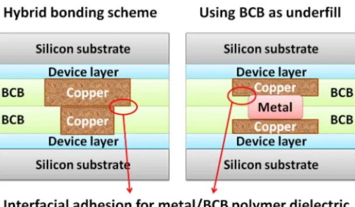
Fig. 1. The interfacial adhesion structure between copper and BCB in (left) hybrid bonding and (right) underfill.
methodology in 3-D IC because it can provide both electrical connection and strength enforcement simultaneously [2], [3].
Regarding the metal and polymer selection for bonding schemes, copper is a widely used metal for interconnection in semiconductor fabrication because of its excellent thermal and electrical properties. In addition, benzocyclobutene (BCB) is a commonly used polymer in semiconductor and packaging industries due to its excellent physical properties such as low curing temperature and high degree of planarization with metal-lization systems. Therefore, the adhesion between Cu and BCB polymers becomes important in two schemes of 3-D integration [4]–[7], as shown in Fig. 1. One is the hybrid bonding scheme, and the other one is using BCB as an underfill. Adhesion mech-anisms are mostly related to the interfacial molecular interac-tions and interfacial chemical structures. However, it is very challenging to inspect interfacial molecular structures without breaking the interface. It is also difficult to investigate buried in-terfaces in situ. The conventional method to investigate a buried interface is to break the samples and analyze the two surfaces to deduce the interfacial chemical structures at the originally buried interface. However, such approach may damage the original interfacial chemical structure and molecular interac-tions, particularly for the interfaces with excellent adhesion.
In recent years, sum frequency generation (SFG) vibrational spectroscopy has been applied to investigate interfaces and surfaces at the molecular level in situ [8]–[12]. SFG vibrational spectroscopy is a second-order nonlinear optical procedure that investigates the second-order nonlinear susceptibility of the material. The selection rules supply SFG interface and
1530-4388 © 2014 IEEE. Personal use is permitted, but republication/redistribution requires IEEE permission. See http://www.ieee.org/publications_standards/publications/rights/index.html for more information.
submonolayer surface sensitivity [13], [14]. Therefore, SFG vibrational spectroscopy becomes a powerful technique for interfacial studies.
SFG vibrational spectroscopy is the only current technique that can provide vibrational spectra at buried interfaces to figure out the interfacial mechanisms. Furthermore, SFG vibrational spectroscopy can be used to examine interfacial molecular interactions and interfacial chemical structures, such as in-terfacial bonding formation, inin-terfacial diffusion, orientation distribution of interfacial functional groups, etc. [15]–[18]. In this paper, we investigate the adhesion strength between copper and BCB polymer dielectric to develop the guidelines for copper and BCB bonding. In addition, since titanium is a com-mon adhesion layer material in metal/metal and metal/oxide dielectric interconnect layers of semiconductor devices [19], the possibility of Ti as the solution for adhesion enhance-ment needs to be investigated in the case of BCB polymer dielectric.
On the other hand, in order to realize the adhesion mecha-nisms between metal and BCB polymer dielectric, SFG vibra-tional spectroscopy is applied to investigate buried interfaces between metal and BCB polymer for a better understanding at the molecular level.
II. EVALUATION OFADHESIONBETWEENCU OR
TILAYER ANDBCB POLYMERDIELECTRIC
A. Experimental Method of Four-Point Bending Test for Ti/BCB and Cu/BCB Interface Layers
As shown in Table I, three groups of samples, metal/BCB polymer layer, are investigated the effect of adding adhesion layer, metal thickness, and layer stacking order. In group 1, a 3-μm-thick BCB polymer film is formed on bare p-type (100)-oriented Si wafers first. Some wafers are then sputtered with a 30-nm-thick Ti layer. Finally, all wafers are sputtered with a 0.2-μm-thick Cu layer. On the other hand, the group-2 wafers are prepared with the same steps as those for group 1, but the thickness of Cu and Ti layers is changed to 1.2 μm and 100 nm, respectively. In order to realize the effect of layer stacking or-der, in group 3, the wafers are prepared by sputtering a 1.2-μm-thick Cu layer first on bare Si wafers. Some wafers are then sputtered with a 100-nm Ti layer. Finally, a 3-μm-thick BCB polymer dielectric is coated on all these wafers.
In this paper, adhesion strength is estimated by a four-point bending test, which can assess the interfacial strength of thin layers [19]. In addition, the four-point bending test can be used to analyze the fracture behavior at the interface and measure the fracture energy of debonding layers to obtain the adhesion strength. The interfacial quantitative fracture-energy value (GC) can be obtained to estimate the physical adhesion
strength from the following expression [20]: GC=
21(1− ν2)P2 CL2 16EB2h3
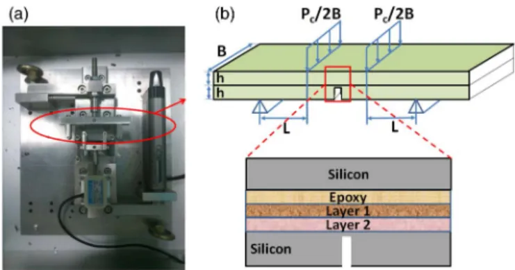
where ν, PC, L, E, B, and h denote the Poisson’s ratio of the silicon substrate (ν) = 0.28, the critical applied force (PC), half the difference of the outer to inner span with the
TABLE I
SCHEMATIC OFTESTSTRUCTURES AND THERESULTS OF
CORRESPONDINGINTERFACIALADHESIONSTRENGTH
loading points (L) = 17.5 mm, Young’s modulus of the silicon substrate (E) = 170 GPa, the sample width (B) = 5 mm, and the half thickness of the sandwich sample (h) = 625 μm, respectively.
Prior to a four-point bending test, each sample from three groups of metal/polymer samples is cleaned and then bond face to face with one bare p-type (100)-oriented silicon samples with the same size (70 mm × 70 mm) through epoxy glue. The bonded samples by epoxy glue are annealed at 150 ◦C for 1 h in nitrogen environment for glue curing. For the four-point bending test, the bonded samples are subsequently diced into dies with 5 mm × 70 mm size, and a notch is created in each bonded sample by dicing at the middle position of the metal layer/BCB polymer dielectric side. Finally, each sample of bonded samples, i.e., 5 mm × 70 mm size, with notch is
Fig. 2. (a) Four-point bending test tool setup. (b) Schematic of the test structure.
prepared for the next four-point bending test. Fig. 2(a) and (b) shows the setup of the four-point bending test and a schematic of the testing structure, where PC/2B is the bending force per unit length.
B. Investigation of the Effects of Adding Adhesion Layer, Metal Thickness, and Layer Stacking Order
After the four-point bending test, X-ray photoelectron spec-troscopy (XPS) and scanning electron microscopy (SEM) are used to investigate the fracture interface location and morphol-ogy. The location of the facture interface can be determined by detecting the composition of copper, titanium, carbon, and silicon elements. Through the evaluation of the four-point bending test, the fracture behavior at the metal/BCB interface can be analyzed. The critical applied force makes the fracture interface of metal/BCB, and the interfacial quantitative fracture energy (GC) can be obtained from the aforementioned formula.
Therefore, the fracture energy can be obtained to evaluate the adhesion strength of each metal/BCB test structure.
Table I shows the measured results of interfacial quantitative fracture energy (GC) for three group samples to investigate
the effect of adding adhesion layer, metal thickness, and layer stacking order. The results from groups 1(a) and 2(a) indicate that increasing the thickness of the copper layer is not a critical factor to affect the interfacial adhesion strength. For all other groups, the extra titanium layer cannot enhance the interfacial adhesion strength between BCB and copper metal, but causes interfacial adhesion strength degradation. It is unexpected that titanium, which is a common adhesion layer material in the interconnect layers of semiconductor IC devices, weakens the interfacial adhesion strength. However, the results from group 3 show that changing the stacking order of copper and BCB polymer can effectively increase the interfacial adhesion strength significantly, and the group 3(a) structure without an extra Ti layer has yielded the best fracture energy result in this study.
In general, the interfacial stress between layers is dependent on the thickness of the metal layer. In this study, the scale of copper layer thickness is small, and the interfacial stress effects between thin films are not obvious [22]. Therefore, the variation of interfacial adhesion strength for groups 1 and 2 is low and about the same quantity.
Fig. 3. (a) Fracture interface of one sample after the four-point bending test. (b) and (c) XPS results of copper and carbon from group 3 without the titanium layer, respectively. (d) Scheme of the fracture path during the four-point bending test.
From the experimental results, since the thermal expansion coefficients of different materials induce the interfacial stress mismatch between different layers, layer stacking order can affect the interfacial adhesion strength significantly. A well-designed layer stacking order for a multilayer structure can minimize the extrinsic stress of mismatch, which can further increase the interfacial adhesion strength [23].
The BCB polymer used in this study is CYCLOTENE 4000 Series advanced electronic resins (photosensitive BCB). In general, BCB polymers have siloxane groups and −CH3,
−CH2−, and >CH− groups in the backbone. Since Si atoms
from the substrate may contaminate the BCB surface during sample preparation, we choose the C atom signal for detecting the BCB polymer. Fig. 3(a) shows the cross-sectional SEM image of the sample Si–Cu(1.2 μm)–BCB(3 μm) (group 3a in Table I) after the four-point bending test. It is clear to show that the BCB polymer and the Cu layer still bond together, which indicates that the interfacial quantitative fracture energy (GC= 11.2 J/m2) comes from the epoxy glue or BCB polymer,
but not the interface between copper and BCB polymer. XPS analysis results show that most interface fractures are located on copper/BCB or titanium/BCB, except for the group 3(a) test structure. As Fig. 3(b) and (c) presents, the XPS results on the fracture interface surface show that the copper element is not detected, but carbon signals containing C–C, C–H, and C–O peaks, which may come from BCB and epoxy glue, are detected. Fig. 3(d) shows the scheme of the fracture path in a strong adhesion Cu/BCB structure during four-point bending.
III. COMPARISONSTUDY OFDIFFERENTMETALS
WITHBCB POLYMER ANDRESULTSFROMSFG VIBRATIONALSPECTROSCOPY
A. Adhesion Investigation of Different Metals With BCB Polymer Dielectric
In order to realize the reason that the interfacial adhe-sion strength of the structure with added adheadhe-sion layer Ti
TABLE II
PROPERTIES OFMETALSTESTED
Fig. 4. Metals tested and corresponding adhesion strength results.
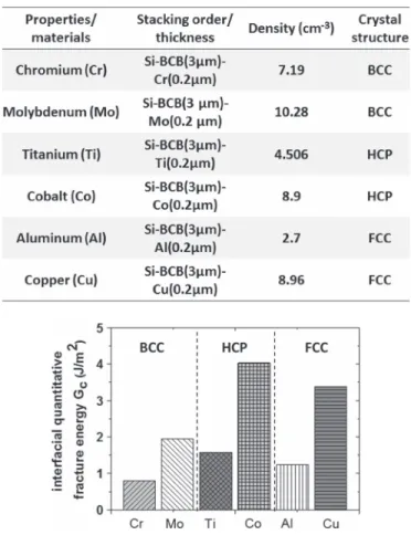
(Si–BCB–Ti–Cu) is significantly lower than that without the titanium layer (which means only the Cu layer on the BCB sample), different metal layers are considered through four-point bending tests with the same layer thickness and stacking order. Table II and Fig. 4 show the interfacial adhesion strengths related to material density and crystal structure. For two metals with the same crystal structure (HCP or BCC or FCC), the one with the higher density has the higher interfacial adhesion strength. It indicates that the interfacial adhesion strength of the BCB polymer and metal layer correlates closely with metal densities of similar crystal structure classification. Therefore, considering the cases of Si/BCB/Cu and Si/BCB/Ti, the interfacial adhesion strength of copper/BCB is larger than that of titanium/BCB. Consequently, using Si–Cu–BCB layer stacking order without the titanium layer for the fabrication of copper/BCB on the silicon wafer can achieve the best adhesion strength and could be adopted in 3-D integration application. B. Interfacial Investigation of Metal/BCB Polymer With SFG Vibrational Spectroscopy
In order to understand the interfacial adhesion mechanisms between copper or titanium and BCB polymer dielectric, SFG vibrational spectroscopy is applied to investigate buried inter-faces between metal and BCB polymer after a cure process. The samples for the SFG data collection have a similar process with the four-point bend test but without the following epoxy
glue bonding process. The correlation between molecular-level chemical structures and physical adhesion strength is also in-vestigated. In this study, a laser beam at 795 nm is generated with a repetition rate of 1000 Hz and energy of 2 mJ/pulse. The 50% of the laser beam is used to produce a narrow-bandwidth 2-ps beam, and the rest is used to pump an optical parametric amplifier (TOPAS-C, Coherent) to generate an IR beam. All SFG spectra in this experiment are collected using the ssp (s-polarized sum frequency output, s-polarized visible in-put, and p-polarized IR input) polarization combination. The 795-nm beam (s-polarized) and the IR beam (p-polarized) are temporally and spatially overlapped on the surface of the sam-ple, with incident angles at 60◦ and 50◦, respectively. Finally, the SFG vibrational spectroscopy signal is detected by a charge-coupled device and collected from the interfaces between the BCB and metal.
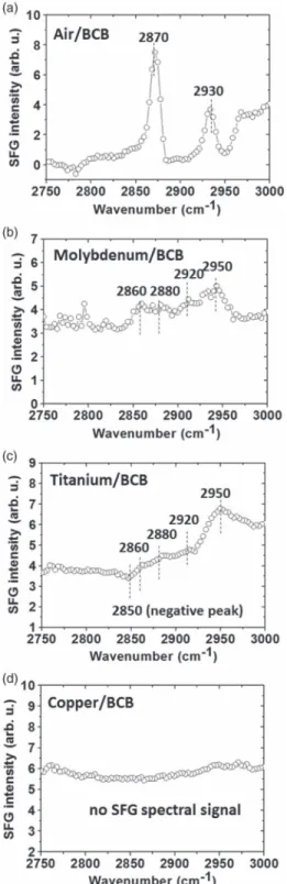
Fig. 5(a) shows the SFG spectrum of an air/BCB interface (3-μm thickness of BCB on Si). Two main peaks are observed at 2870 and 2930 cm−1, which are consistent with the methyl group symmetric C–H stretching mode and the Fermi resonance [18], [24].The SFG spectral results indicate that the methyl groups are ordered at the air/BCB interface. The general C–H spectral range, i.e., 2800–3000 cm−1, can be detected through SFG vibrational spectroscopy [16]–[18], [24].
The location of one C–H spectral peak is determined by the interference of resonant modes. Therefore, C–H spectral peaks at different locations may be detected in each individual case [18], [24]. Fig. 5(b) and (c) shows the SFG spectra of molyb-denum/BCB and titanium/BCB interfaces, respectively. Both SFG spectral signals show strong peaks at∼2950 cm−1in the C–H range at the interface of molybdenum/BCB and titanium/ BCB, due to the methyl Fermi resonance [24]. The peak at 2880 and 2860 cm−1 can be observed, indicating that methyl groups C–H symmetric stretching and Fermi resonance are ordered at the interface [24], [25]. Another peak at 2920 cm−1 can also be observed, revealing that methylene groups are also ordered at the metal/BCB interface [24]. These SFG spectral results show that after depositing the molybdenum and titanium layer, the C–H groups still remain in order at the metal/BCB interface. In addition, a peak at 2850 cm−1(negative peak) is detected in the case of titanium/BCB because of methylene symmetric stretching [24], [26]. Due to interference between resonant and nonresonant contributions or between contribu-tions from different resonant modes, the resonant peaks in the SFG spectra (from a metal/polymer interface) may appear neg-ative or asymmetric [18]. In fact, the significance values of the positive and negative peaks are the same. Their main difference is the order direction. Furthermore, the small positive or neg-ative peak could be considered that an extreme small amount of C–H groups is ordered at the interface or system noise.
However, in the range of C–H spectrum, no SFG spectral signal can be detected from the interface of copper and BCB polymer, indicating an interfacial disordering in Fig. 5(d). Comparing Fig. 5(b), (c), and (d), it is clear that the C–H groups of BCB are observable at the interfaces of titanium/BCB and molybdenum/BCB, whereas it is undetectable at the copper/ BCB interface. It demonstrates that the BCB polymer main-tains certain ordering at the interfaces of molybdenum/BCB
Fig. 5. SFG spectrum of (a) air/BCB, (b) Mo/BCB, (c) Ti/BCB, and (d) Cu/ BCB interfaces.
and titanium/BCB but becomes disordered at the copper/BCB interface. The ordering change of BCB upon deposition of the copper film is an indication that there is a stronger interaction between copper and BCB, which is consistent with the above four-point bending test.
In this paper, the direction of C–H groups at the Cu/BCB interfaces may be changed from toward the copper layer to the interface. However, for the molybdenum or titanium layer, the C–H groups can be contributed from different resonant
modes without excluding the C–H groups from the metal layer. On the other hand, we agree that the possibility of the Cu atom diffusing and migrating into the BCB layer should be considered. It is really possible that the interfacial boundary between Cu and BCB may be blurred from Cu atom diffusion, which results in the disorder of C–H groups. However, these assumptions need to be further investigated as well as the adhesion mechanism among metal/BCB.
Furthermore, the surface roughness and inherent chemical nature should be considered in interfacial adhesion strength investigation. The surface roughness may be one of key factors about interfacial adhesion. The adhesion mechanism of surface roughness is similar to a mechanical interlock action, and the effect of mechanical interlock on adhesion strength with surface roughness has been discussed in detail in the previous study [27].
Another possible factor is the inherent chemical nature of polymer, which needs to be evaluated considering other types of polymer dielectric materials. In this paper, since BCB is a commonly used polymer in semiconductor and packaging industries, we focus on the interfacial chemical property for metal/BCB with considering the ordering of C–H groups. In order to effectively study the interfacial polymer group ordering with the aid of SFG vibrational spectroscopy, further research need to be carried out with other types of polymer dielectric materials such as SU8 and polyimide.
IV. CONCLUSION
Interfacial adhesion strength between metals and BCB poly-mer dielectric has been investigated using the four-point bend test method in this paper. The layer stacking order for the test structure was found to impact the adhesion strength between metal and BCB layers. The addition of a Ti layer between Cu and BCB showed poor interfacial adhesion strength. An in-crease in adhesion strength was observed with metals of higher material density and crystal order. In addition, SFG vibrational spectral results were useful in understanding the interfacial adhesion behaviors between metals and BCB layers through the ordering of C–H organic groups in the BCB polymer dielectric material. The presence of such molecular ordering in the case of Mo/BCB and Ti/BCB interfaces showed poor adhesion. On the other hand, negligible SFG spectral signal in the case of the Cu/BCB interface corresponds to disordering of the BCB organic groups, which promotes improved adhesion.
ACKNOWLEDGMENT
The authors would like to thank National Chiao Tung Univer-sity for the facility assistance in using the fabrication facilities.
REFERENCES
[1] J. Q. Lu, “3-D hyperintegration and packaging technologies for micro–nano systems,” Proc. IEEE, vol. 97, no. 1, pp. 18–30, Jan. 2009. [2] R. S. Patti, “Three-dimensional integrated circuits and the future of
system-on-chip designs,” Proc. IEEE, vol. 94, no. 6, pp. 1214–1224, Jun. 2006.
[3] P. Garrous, Handbook of 3D Integration: Technology and Applications of
[4] C. T. Ko and K. N. Chen, “Wafer-level bonding/stacking technology for 3D integration,” Microelectron. Rel., vol. 50, no. 4, pp. 481–488, Apr. 2010.
[5] M. Lapisa, G. Stemme, and F. Niklaus, “Wafer-level heterogeneous in-tegration for MOEMS, MEMS, NEMS,” IEEE J. Sel. Topics Quantum
Electron., vol. 17, no. 3, pp. 629–644, May/Jun. 2011.
[6] Y. Sun, X. Li, J. Gandhi, S. Luo, and T. Jiang, “Adhesion improvement for polymer dielectric to electrolytic-plated copper,” in Proc. Electron.
Compon. Technol. Conf., Las Vegas, NV, USA, 2010, pp. 1106–1111.
[7] L. Dumas et al., “Electromigration and adhesion improvements of Thick Cu/BCB architecture in BiCMOS RF technology,” in Proc. WSEAS
Int. Conf. Microelectron., Nanoelectron., Optoelectron., Mar. 2006,
pp. 138–141.
[8] Y. R. Shen, “Surface properties probed by second-harmonic and sum-frequency generation,” Nature, vol. 33, pp. 519–5257, Feb. 1989. [9] S. Baldelli, “Surface structure at the ionic liquid–electrified metal
inter-face,” Accounts Chem. Res., vol. 41, no. 3, pp. 421–431, 2008.
[10] P. L. Hayes, A. R. Keeley, and F. M. Geiger, “Structure of the cetyltrimethylammonium surfactant at fused silica/aqueous interfaces studied by vibrational sum frequency generation,” J. Phys. Chem. B, vol. 114, no. 13, pp. 4495–4502, Mar. 2010.
[11] S. Kataoka and P. S. Cremer, “Probing molecular structure at interfaces for comparison with bulk solution behavior: Water/2-propanol mixtures monitored by vibrational sum frequency spectroscopy,” J. Amer. Chem.
Soc., vol. 128, no. 16, pp. 5516–5522, Apr. 2006.
[12] G. J. Holinga et al., “An SFG study of interfacial amino acids at the hydrophilic SiO2 and hydrophobic deuterated polystyrene surfaces,”
J. Amer. Chem. Soc., vol. 133, no. 16, pp. 6243–6253, Mar. 2011.
[13] A. J. Moad and G. J. Simpson, “A unified treatment of selection rules and symmetry relations for sum-frequency and second harmonic spectroscopies,” J. Phys. Chem. B, vol. 108, no. 11, pp. 3548–3562, Feb. 2004.
[14] C. Hirose, N. Akamatsu, and K. Domen, “Formulas for the analysis of the surface SFG spectrum and transformation coefficients of Cartesian SFG tensor components,” Appl. Spectroscopy, vol. 46, no. 6, pp. 1051–1072, Jun. 1992.
[15] C. Y. Chen, J. Wang, C. L. Loch, D. Ahn, and Z. Chen, “Demonstrating the feasibility of monitoring the molecular-level structures of moving polymer/silane interfaces during silane diffusion using SFG,” J. Amer.
Chem. Soc., vol. 126, no. 4, pp. 1174–1179, Jan. 2004.
[16] Z. Chen, “Understanding surfaces and buried interfaces of polymer ma-terials at the molecular level using sum frequency generation vibrational spectroscopy,” Polymer Int., vol. 56, no. 5, pp. 577–587, May 2007. [17] C. Y. Chen, J. Wang, M. A. Even, and Z. Chen, “Sum frequency
gen-eration vibrational spectroscopy studies on “buried” polymer/polymer interfaces,” Macromolecules, vol. 35, pp. 8093–8097, Sep. 2002. [18] Z. Chen, “Investigating buried polymer interfaces using sum frequency
generation vibrational spectroscopy,” Progr. Polymer Sci., vol. 35, no. 11, pp. 1376–1402, Nov. 2010.
[19] G. A. Somorjai and Y. Li, Introduction to Microfabrication. Hoboken, NJ, USA: Wiley, 2010.
[20] J. J. McMahon, J. Q. Lu, and R. J. Gutmann, “Wafer bonding of damascene-patterned metal/adhesive redistribution layers for via-first three-dimensional (3D) interconnect,” in Proc. 55th ECTC, 2005, pp. 331–336.
[21] T. Usami, C. Maruyama, M. Tagami, K. Watanabe, and T. Kameshima, “A study of adhesion and improvement of adhesion energy using hybrid low-K (proous-Par/porous-SiOC (k = 2.3/2, 3)) structures with multi-layered Cu interconnects for 45-nm node devices,” in Proc. IEEE Int.
Interconnect Technol. Conf., Jun. 2007, pp. 96–98.
[22] R. C. Cammarata, “Surface and interface stress effects in thin films,”
Progr. Surface Sci., vol. 46, no. 1, pp. 1–38, May 1994.
[23] C. D. Hartfield, E. T. Ogawa, Y. J. Park, T. C. Chiu, and H. Guo, “Interface reliability assessments for copper/low-k products,” IEEE Trans. Device
Mater. Rel., vol. 4, no. 2, pp. 129–141, Jun. 2004.
[24] C. Zhang, J. Hankett, and Z. Chen, “Molecular level understanding of adhesion mechanisms at the epoxy/polymer interfaces,” ACS Appl. Mater.
Interfaces, vol. 4, no. 7, pp. 3730–3737, Jun. 2012.
[25] G. A. Somorjai and Y. Li, Introduction to Surface Chemistry and
Catalysis. Hoboken, NJ, USA: Wiley, 2010, p. 588.
[26] M. Oh-e, A. I. Lvovsky, X. Wei, and Y. R. Shen, “Sum-frequency gen-eration (SFG) vibrational spectroscopy chain structures of polyimide sur-faces,” J. Chem. Phys., vol. 113, no. 19, p. 8827, 2000.
[27] W.-S. Kim, I.-H. Yun, J.-J. Lee, and H.-T. Jung, “Evaluation of mechan-ical interlock effect on adhesion strength polymer–metal interfaces using micro-patterned surface topography,” Int. J. Adhesion Adhesives, vol. 30, no. 6, pp. 408–417, Sep. 2010.
Jian-Yu Shih received the B.S. degree in electronics engineering from National Chung Hsing University, Taichung, Taiwan, in 2009. He is currently working toward the Ph.D. degree in the Department of Elec-tronics Engineering, National Chiao Tung Univer-sity, Hsinchu, Taiwan.
The focus of his research studies includes through-silicon via, hermetic bonding, heterogeneous inte-gration, frequency electronic packaging, and 3-D integrated circuit technologies.
Wen-Chun Huang received the M.S. degree in electronics engineering from the Department of Electronics Engineering, National Chiao Tung Uni-versity, Hsinchu, Taiwan, in 2013.
Since 2013, he has been with the Depart-ment of Device DevelopDepart-ment, Nuvoton Technology, Hsinchu. The focus of his research studies includes wafer-level bonding, heterogeneous integration, and 3-D integrated circuit technologies.
Cheng-Ta Ko received the B.S. and M.S. degrees in chemical engineering from National Taiwan Univer-sity, Taipei, Taiwan, in 2000 and 2002, respectively. He is currently working toward the Ph.D. degree in the Department of Electronics Engineering, National Chiao Tung University, Hsinchu, Taiwan.
Since 2002, he has been with the Electronics and Optoelectronic Research Laboratories, Industrial Technology Research Institute, Hsinchu, where he is currently a Manager in the Packaging Technology Division. The focus of his research studies includes wafer-level packaging, system in package technology, flexible electronic pack-aging, and 3-D integrated circuit technologies.
Zheng Yang received the Ph.D. degree in physical chemistry from the Univer-sity of British Columbia, Vancouver, BC, Canada, in 2011.
He is currently a Postdoctoral Research Fellow at The University of British Columbia.
Sheng-Hsiang Hu received the M.S. degrees in materials science and engineer-ing from National Chiao Tung University, Hsinchu, Taiwan, in 2012.
Jihperng Leu received the B.S. degree from Na-tional Tsing Hua University, Hsinchu, Taiwan, in 1980; the M.S. degree from the University of Florida, Gainesville, FL, USA, in 1984; and the Ph.D. de-gree from the University of Minnesota, Twin Cities, Minneapolis, MN, USA, in 1990, all in chemical engineering.
He was a Visiting Scientist with the Thomas J. Watson Research Center, IBM Corporation, Yorktown Heights, NY, USA, from 1990 to 1991 and a Research Associate with the University of Texas at Austin, Austin, TX, USA, from 1992 to 1994. In 1994, he joined Motorola, Inc., as a Project Manager at SEMATECH for the low-k program. From 1997 to 2004, he was with Intel Corporation, Hillsboro, OR, USA, as a Group Leader in Components Research, working on back–end interconnects and integration. He is currently a Professor with the Department of Materials Science and Engineer-ing, National Chiao Tung University, Hsinchu, Taiwan. He has authored more than 40 publications and coauthored two books and conference proceedings. He holds 27 U.S. and several international patents. His research interests involve thermomechanical reliability, porous low-k dielectrics, and flexible devices in semiconductor and optoelectronic applications.
Dr. Leu is a member of the Electrochemical Society, the Materials Research Society, and the Society for Information Display.
Keng C. Chou received the Ph.D. degree in physics from the University of California, Riverside, CA, USA, in 2001.
From 2001 to 2004, he was a Postdoctoral Fellow with the University of California, Berkeley, CA. He is currently an Associate Professor of chemistry with the University of British Columbia, Vancouver, BC, Canada. His research focus includes optical spec-troscopy and microscopy.
Kuan-Neng Chen (M’05–SM’11) received the Ph.D. degree in electrical engineering and computer science, in 2005 and the M.S. degree in materials sci-ence and engineering from Massachusetts Institute of Technology, Cambridge, MA, USA.
He is currently a Professor with the Department of Electronics Engineering, National Chiao Tung University, Hsinchu, Taiwan. Prior to the faculty position, he was a Research Staff Member with the IBM Thomas J. Watson Research Center, Yorktown Heights, NY, USA. He has authored more than 180 publications and holds 61 patents. He has given more than 50 invited talks in industries, research institutes, and universities worldwide. His current re-search interests include 3-D integrated circuits, through-silicon via technology, wafer bonding technology, and heterogeneous integration.
Dr. Chen has received four times the National Chiao Tung University (NCTU) Distinguished Faculty Award, three times the NCTU Outstanding Industry—Academia Cooperation Achievement Award, the Adventech Young Professor Award, the Chinese Institute of Electrical Engineering Outstanding Youth Engineer Award, and the Electronics Devices and Materials Association Outstanding Youth Award. He also holds five IBM Invention Plateau Invention Achievement Awards. He is currently a committee member of the IEEE Inter-national Conference on 3D System Integration, the IEEE InterInter-national Confer-ence on Solid State Devices and Materials, the International Microelectronics Assembly and Packaging Society 3D Packaging, and Dry Process Symposium (DPS). He is a member of the Phi Tau Phi Scholastic Honor Society.