in which the MOS transistors are biased in subthreshold region with a supply voltage and current of 0.4–0.8 V and 0.23–1.86 A, respectively, to reduce the system power. Flicker noise is then removed using a chopping technique, and differential interference produced by electrode impedance imbalance is suppressed using a Gm-C filter. Additionally, the circuit is fabricated using TSMC 0.18 m CMOS technology with a core area of 0.77 0.36 mm . With a minimum supply voltage of 0.4 V, the measured SNR and power consumption of the proposed IC chip are 54.1 dB and 0.09 W, respectively.
Index Terms—Biopotential recording, chopper amplifier, flicker noise, instrumentation amplifier.
I. INTRODUCTION
I
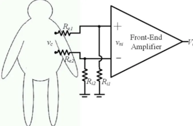
NTEGRATED CIRCUIT (IC) design has increasingly focused on lower power consumption, lower voltage and miniaturized size, contributing to the development of biomed-ical device [1]–[12]. Reducing the area diminishes the size and weight of electronic devices, making it more user-friendly. Low voltage and low power dissipation are essential to increasing battery lifetime in electronic devices. However, low power and low voltage correspond to poor noise immunity, especially when the device includes analogue circuitry. An important source of noise encountered in low-power and low-voltage biomedical devices is flicker (or ) noise, which is associated with the circuitry of an operational amplifier (OPAMP) [13], [14].Beside the flicker noise, the biotelemetry systems based on biosignal recording, including ECG, EEG, and EMG, also incur severe electrical interferences, owing to its lack of a ground electrode. Fig. 1 illustrates a simplified circuit model of the biotelemetry system. Where and denote the electrode resistors, and represent the input resistances of a front-end amplifier constructed by an instrumentation amplifier Manuscript received March 21, 2011; revised August 24, 2011 and November 25, 2011; accepted February 03, 2012. Date of publication March 21, 2012; date of current version November 28, 2012. This work was supported by the National Science Council and the Ministry of Education, Taiwan. This paper was recommended by Associate Editor T. Denison.
The authors are with the Electrical Engineering Department and Institute of Electrical Control Engineering, National Chiao Tung University, Hsinchu 300, Taiwan (e-mail: yuhwaitseng@mail.nctu.edu.tw).
Color versions of one or more of the figures in this paper are available online at http://ieeexplore.ieee.org.
Digital Object Identifier 10.1109/TBCAS.2012.2188029
Fig. 1. A simplified circuit model of the biotelemetry system.
(IA). Interference [15]–[18] at the input of the front-end amplifier for biotelemetry recording is simplified as
(1) Where refers to the common mode noise, mainly including static charge of the human body and 60 Hz noise from the power line. CMRR is the common mode rejection ratio of the front-end amplifier. Where and denote the difference impedance between two input electrodes and the common mode input impedance of the front-end amplifier. Interference of the IA includes the common and differential mode interference represented by the first and second terms of (1), respectively.
Many effective methods had been developed in recent decades to reduce or cancel out the dominant noise of the front-end amplifier of the biotelemetry [19]–[25]. The chopper method is one of the most effective means of reducing the flicker noise, and has been widely developed in the low power analog circuitry design of bio-signal recording systems [26]–[34]. Regarding the , (1) indicates that increasing the CMRR and of the front-end amplifier and reducing of the two electrodes cancel out the .
In addition to the noise cancellation problem, designing a low power and low voltage system based on the current VLSI cir-cuit approach is also limited in a conventionally adopted method in which MOS transistors are designed to operate in saturation mode. This work design a low-power and low-noise front-end biopotential amplifier IC based on an approach in which the MOS circuits operate in a subthreshold region. A chopper-sta-bilized instrumentation amplifier proposed elsewhere [26]–[29] 1932-4545/$31.00 © 2012 IEEE
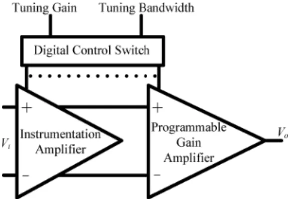
Fig. 2. Architecture of the front-end biopotential amplifier.
is adopted to reduce the flicker noise. Additionally, the common and differential mode interference caused by a mismatch of the impedance of the two input electrodes for telemetry systems is analyzed using a simplified model. Moreover, a wide range of biopotential signals is recorded using a programmable gain am-plifier (PGA), thus providing the proposed front-end amam-plifier design with a tunable gain and a wide application bandwidth.
II. DESIGN OFFRONT-ENDBIOPOTENTIALAMPLIFIERIC Fig. 2 schematically depicts the front-end biopotential ampli-fier, which consists of an instrumentation amplifier (IA), a pro-grammable gain amplifier (PGA), and digital control interface. The IA amplifies the signal with a strong rejection of interfer-ence. To accommodate the recording of the various biopotential signals, the programmable gain amplifier offers a variable gain and a bandwidth that is controlled via a digital switch.
A. The Chopper Stabilized IA With Common Mode Interference Cancellation
Flicker noise is concentrated in low-frequency bands and arises from the channel of the MOS transistor, since the icon crystal at the interface between the gate oxide and the sil-icon substrate in the MOSFET is imperfect. The chopper tech-nique efficiently reduces the flicker noise in the design of an analog circuit. Fig. 3 displays diagram of chopper IA with a common mode interference cancellation scheme. The chopper IA comprises an OPAMP, a low pass filter, three multipliers, which are controlled by a chopping square wave of with values and , and a chopper feedback function with a loop gain of 1/K. The terms and denote the system input and output signals, respectively; represents common mode in-terference; denotes an estimated common mode interfer-ence, and is the flicker noise of the amplifier.
The and are modulated to the odd harmonic fre-quency of the square waveform of the chopper using the first multiplier. The modulated and are mixed with . Then, the amplifier and second multiplier amplify and demodulate back to the original signal band, respectively, and is modulated to the high-frequency band. Finally, the system output signal is given by
(2)
Fig. 3. Diagram of a chopping IA with a common mode interference cancella-tion.
Fig. 4. Circuit diagram of the proposed IA.
TABLE I
VALUE OF THERELATEDPARAMETERS INFIG. 4
Where represents the being amplified by a gain
factor of A. The third term of the (2) indicates that the estimated , extracted from by a low pass filter and a chopper feedback loop, is applied to cancel the .
Fig. 4 shows the circuit diagram of the proposed IA. Table I presents the values of the related parameters in Fig. 4. To reduce the common mode voltage and thermal noise, a chopper-stabi-lized amplifier with a Gm-C feedback filter was developed. The bootstrapped NMOS chopper is adopted in the system since a low power and low voltage are required.
The proposed IA has two feedback paths: one provides the close-loop gain of the system via feedback capacitors , while the other cancels out the interference that is caused by the common mode voltage and the mismatch of the impedance of the two input electrodes, which is extracted by a Gm-C filter and via feedback capacitors . The two feedback paths were formed from capacitors, because the capacitive closed-loop configuration dissipates less power than the resistive feedback one. The output voltages of the proposed IA are
(3) (4)
Fig. 6. Circuit diagram of the proposed OPAMP.
Where , and represent the differential and common mode open loop gain of the OPAMP, respectively. The differential and common mode gain ( and ) of the proposed IA can be derived as
(5)
(6) Equations (5) and (6) describe a high pass filter with 3 dB high
pass poles of ( and
. Fig. 5 plots the differential and common mode gain as function of frequency. The results indicate that the CMRR of the system exceeds 125 dB when signal frequency below 10 kHz.
B. Operational Amplifier
Fig. 6 schematically depicts the circuit diagram of the OPAMP used in design of the proposed IA. The OPAMP com-prises a fully differential folded-cascode amplifier with two choppers and a common mode feed back (CMFB) circuit. The PMOS transistors are utilized in the input circuit to reduce the flicker noise and the circuit mismatch caused by the process variation, increase the range of the input common
Fig. 7. Circuit diagram of the OTA.
mode voltage. The proposed mixer is then constructed using a
group of the PMOS and NMOS
chopping switches to eliminate the residual offset of the cir-cuit. This work also develops a novel continuous time CMFB
( , and ) with a long channel
PMOS-resistor to reduce the degradation of the open loop gain in the conventional CMFB circuit with a resistance voltage divider. The long channel PMOS pseudo-resistors are implemented as a light loading circuit with a bias current below 20 nA which reduce the effect upon the swing of the OPAMP especially for the low speed input signal.
To maximize the loop gain and minimize the power of the IA system, the MOS transistors are biased to operate in the re-gion of the weak inversion. Consequently, the open loop gain, common mode gain and unit gain bandwidth are 68 dB, dB and 100 kHz, respectively.
By using an operational transconductance amplifier (OTA) with a fully differential current-mirror, this work constructs a Gm filter since the performance of the OTA circuit is less sensi-tive to the process variation. Fig. 7 shematiclly depicts the OTA circuit.
To ensure a stable operation, this work designs the dominant pole of the OTA circuit at the output node to increase its time constant. The output of the OTA circuit is connected to an ex-ternal capacitor with a capacitance of 0.33 F in order to form a low pass filter with a 3 dB frequency of 0.5 Hz, thus dimin-ishing the interference caused by an imbalance of the electrode impedance.
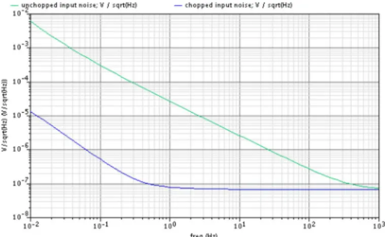
Fig. 8 presents an input-referred noise density of the pro-posed IA circuit by using the Cadence Spectre tool. The thermal noise floor is 70 nV/ . The amount of the flicker noise is inversely proportional to the frequency below the corner fre-quency of around 1 kHz. The upper line of the figure presents an input-referred noise of 10000 nv/rtHz without using the chop-ping method and the lower line 73 nv/rtHz when activating the chopping method. Fig. 8 indicates that the chopping method re-duces the flicker noise of the IA system several hundred times than without using the chopping method.
C. Programmable Gain Amplifier
Owing the significant variation in the amplitudes of biopo-tential signals, an amplifier can be designed with a tunable gain to satisfy the specification. Here, such a tunable gain is pro-vided using a PGA. Fig. 9 illustrates the PGA, which is a ca-pacitive differential amplifier that consists of a single-end cur-rent-mirror OTA with a capacitive gain feedback, pseudo
resis-Fig. 8. Input-referred noise density by Cadence Spectre.
Fig. 9. Circuit diagram of the PGA.
tors made from PMOS transistor, and switches for tuning the gain. The gain selector is made from 12 capacitors of the same type, providing variable gains of 0, 6 and 30 dB. The band-width selector consists of 3 capacitors made by NMOS tran-sistors, which produce system 2 selectable frequency bands of 0.5–100 and 10–400 Hz. During blocking the DC offset, a high pass filter with an extremely low 3 dB frequency is established using the positive terminal feedback path. The differential gain of the PGA system can be derived as
(7)
A selectable was employed to control the system gain.
When , the differential gain is .
The maximum variable gain of the PGA is set to 30 dB.
D. Fully-Differential Boosted Clock Driver
A residual offset voltage is introduced due to the charge injec-tion of the MOS switches in the chopper IA circuit. The residual offset voltage can be derived as
(8)
Fig. 10. (a) Circuit diagram of the proposed fully-differential boosted clock driver. (b) Logic diagram of the non-overlapped clock generator.
Where is the chopping frequency, is the spike magni-tude due to the charge injection of the input MOS switches, and refers to the settling time constant of the OPAMP. However, according to (8), a smaller and lower can reduce the yet also increase the power consumption and the flicker noise of the IA system.
Applying a fully-differential boosted clock driver reduces and increase the output clock voltage from to 2 without consuming the system power. Fig. 10(a) shows the circuit diagram of the proposed fully-differential boosted clock driver. Fig. 10(b) illustrates the logic diagram of the proposed non-overlapped clock generator composed of NOR gates and inverter chains. All of the circuits in the proposed non-overlapped clock generator are designed using standard cells of minimal sizes since the is a low speed clock below several kilo hertz. Notably, the must be designed larger than the corner frequency 1 kHz shown in Fig. 8 to increase the system SNR. Based on Fig. 8 and (8), the 4 kHz chopper frequency is applied in the proposed IA circuit, which capable of reducing the and the flicker noise and with a 3 kHz spacing frequency from the corner frequency suitable for boisignal recording.
III. COMMON ANDDIFFERENTIALMODEINTERFERENCE REJECTION IN THEPROPOSEDIA
A simplified circuit model shown in Fig. 11 is applied to cal-culate the interference of the proposed amplifier under various conditions. is the capacitance between the power line and the human body; represents the noise current that is cou-pled from the power line into the human body; is the noise of the static charge on the human body; denotes the input noise of the circuit; and are the capacitance from the human body and the amplifier to the ground, respectively;
Fig. 11. A simplified circuit model for the proposed IA.
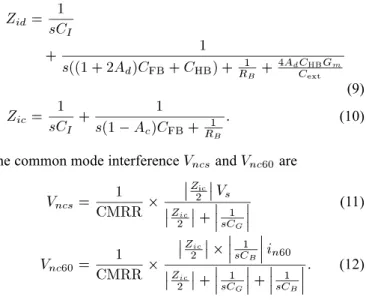
represents the input equivalent impedance of the IA which in-cludes the common mode input impedance and the differ-ential mode input impedance . and are derived as
(9) (10)
The common mode interference and are
(11)
(12) With the impedance mismatch of the input electrodes, a very large differential mode interference, to which the common mode interference contributes, will be coupled into the proposed cir-cuit, reducing SNR (signal to noise ratio) of the system. There-fore, the differential mode interference and due to
and , respectively, can be obtained as
(13)
(14)
Figs. 12 and 13 plot the noise level of the proposed amplifier, obtained from (11)–(14), for various values of and . These plots indicate that the proposed amplifier suffer max-imum common mode and differential mode interference of less than
Fig. 12. Estimated results of common mode interference for the proposed IA.
Fig. 13. Estimated results of differential interference for the proposed IA.
Fig. 14. Die photo of the proposed front-end biopotential amplifier IC. 0.35 pV and 0.85 mV, respectively, in the worst case with
V and A, k . Hence, the IA has
high CMRR and input impedance with greater immunity to interference.
IV. IMPLEMENTATION ANDMEASUREMENT
The proposed front-end amplifier is fabricated using TSMC 0.18 m CMOS technology. Fig. 14 presents a die photograph, including an IA circuit with a GM-C filter, a PGA, output buffers and MOS capacitors. The chip area is 1.03 0.62 mm and the core area is 0.77 0.36 mm .
A. Measurement of the Human Body Noise
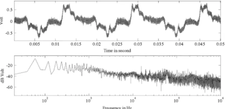
During measurement of the human body noise, the left wrist of the human body and Agilent-54832D oscilloscope are con-nected by applying one electrode (Kendall H99SG). Fig. 15 shows the measurement results of the human body noise and its frequency spectrum. The frequency spectrum indicates that the main noise sources of the human body are below 10 kHz, composed mainly of the 60 Hz power line noise and its har-monics. The measured human body noise with an amplitude of mV is coupled into the IA system by using the form
Fig. 15. The measured human body noise (measured by Agilent Oscilloscope 54831D).
Fig. 16. The simulation and measurement results of the CMRR.
of common and differential mode as shown in (1), which satu-rates the front-end amplifier of the IA system and significantly reduces the system SNR.
B. CMRR Measurement Result of the Proposed IA
By using 12 test stimuli, this work measures the CMRR of the proposed front-end amplifier with V sinusoidal signals ranging from 20 Hz to 100 kHz. The test stimulus are then gen-erated and received by using an Agilent 33250A wave gener-ator and an Agilent E4440 RF spectrum analyzer, respectively. The supply voltage of the proposed front-end amplifier is set to 0.4 V to bias the MOS transistors operating in the subthreshold region. Fig. 16 summarizes the simulation (from (5)–(6)) and measurement results of the CMRR. According to this figure, the measured result of the CMRR closely resembles the calculated results derived from (5)–(6). The maximum difference between the calculation and measurement results is dB when the signal frequency is 100 kHz. The minimum CMRR is larger than 125 dB, which is sufficient to reject the common and differen-tial mode noise shown in (1) and Fig. 1.
C. Measurement of the 60 Hz Differential Interference Arising Due to Impedance Mismatch of the Input Electrodes
This work measures how 60 Hz differential interference arises due to impedance mismatch of the two electrodes and affects the proposed analog front-end amplifier. A variable re-sistor is connected between the positive input terminal of the IA circuit and its electrode, subsequently providing an impedance mismatch , shown as the second term of (1) from 0 to 100 k . The two electrodes are then connected together and placed on the right wrist that mimics the environment, as shown in Fig. 11. Next, the 60 Hz body noise with a noise current of about 0.7 A (peak-to-peak) becomes differential noise coupled into the IA circuit. Additionally, the output noise
Fig. 17. Measurement result of the 60 Hz differential noise.
Fig. 18. Photo of the measurement setup.
amplitude of the IA circuit is measured using an agilent E4440 RF spectrum analyzer. Fig. 17 shows the measurement results of the 60 Hz differential noise due to impedance mismatch of the two electrodes of the front-end amplifier with a different . According to (1)–(5), the measurement result indicates that increasing will increase the amount of the body noise into the IA circuit. The maximum 60 Hz differential input noise of the IA is only 4.5 mV when equal 100 k since high input impedance exists at the input of the proposed IA circuit which is the same as the description of the (13) and (14).
D. Measurements of ECG, EEG, and EMG
Feasibility of the proposed approach is verified by estimating the SNR of an ECG signal first, and then measuring EEG and EMG signal, respectively. Fig. 18 displays the experimental setup. Two electrodes (Kendall H99SG) connect the measured body directly to the input of the proposed front-end amplifier. Next, the ECG signal is obtained from the proposed front-end amplifier by using an Agilent 54831D mixed-signal oscillo-scope, at a sampling rate of 400 kHz, subsequently yielding 2M data points at a time interval of 5 second. The Keithley 2400 source meter employs to measure the dissipated current and power of the proposed amplifier.
Fig. 19 plot the ECG measurement made by using different supply voltages ( V, 0.6 V and 0.4 V) and the same in the frequency domain, respectively. The voltage gain of the pro-posed IC circuit is set to 40 dB, and the output amplitude of the ECG is 270 mV. According to these figures, although no static charge or 60 Hz interference occurs in the circuit, some flicker noise is modulated to high frequency and the intrinsic noise of the oscilloscope is present with a maximum peak-to-peak voltage of 10 mV. The proposed IC chip achieves a dynamic range (1% THD) of 61 dB with a total power current of 0.226 A under a supply voltage of 0.4 V.
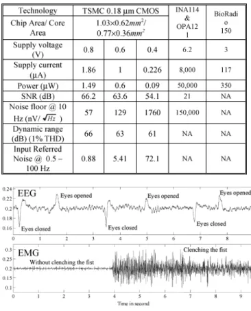
Fig. 20 illustrates the ECG measured results of a commer-cial bio-signal recording amplifier generally made by INA114
Fig. 19. ECG recording and frequency spectrum results of the proposed front-end amplifier.
Fig. 20. The ECG measured results of a commercial bio-signal recording am-plifier made by INA114 and opa121.
and opa121, in which 60 Hz and 8.25 kHz noise occurs in the recording amplifier under a high noise floor 150 and peak-to-peak voltage of 100 mV. This finding suggests that the amount of the CMRR and the input impedance of the commer-cial recording amplifier are insufficient to reject the 60 Hz power line noise. The measured SNR is 21 dB with a supply voltage of 6.2 V and total power consumption of 50 mW. Fig. 21 shows an ECG measurement result of a commercial telemetry biopo-tential recorder (BioRadio150 made by Cleveland Medical De-vices Inc.) with a 3 V supply voltage and 350 W power con-sumption [35]. Table II summarizes the performance of the pro-posed amplifier and the commercial biopotential recorder, indi-cating the proposed amplifier performs better than the commer-cial biopotential recorder (BioRadio150) in power consumption and the commercial bio-signal recording amplifier (INA114 and opa121) in all respect.
This work also measure EEG and EMG signals by placing two electrodes on the occipital lobe and the right forearm, re-spectively. The two electrodes are about 2 cm apart from each other. The sampling rate of the Tektronix TPS 2024 oscilloscope is set to 500 Hz. Fig. 22 shows the measurement results of a
Fig. 21. The ECG measured results of a commercial telemetry recording system-BioRadio150 made by Cleveland Medical Devices Inc.
TABLE II
PERFORMANCES OF THEPROPOSEDIC CHIP
Fig. 22. The measurement results of the EEG and EMG signal.
wave of EEG with eyes opened and eyes closed control signal, as well as an EMG signal of the right forearm with and without clenching the fist, respectively. Based on those results, max-imum peak-to-peak amplitude of 40 mV and 100 mV of EEG and EMG signal are measured, respectively, under maximum noise peak-to-peak amplitude of 8 mV from the intrinsic noises of the oscilloscope.
Measurement results of ECG, EEG and EMG signal verify the CMRR, and the input impedance of the proposed front-end biopotemtial amplifier is sufficiently large to reject the common and differential interference significantly, which is suitable for a biosignal recording system. Table III summarizes the perfor-mance and comparison results of the bio-potential front-end am-plifier.
V. CONCLUSION
A low power front-end biopotential amplifier IC that can be adopted in biosignal recording is implemented. The MOS tran-sistors in the proposed IC are operating in subthreshold region to reduce the system power. Chopping technique is applied to remove the flicker noise in the MOS circuit into the high fre-quency band. A Gm-C filter is utilized to detect and cancel out the differential interference that was generated by imbalance of the electrodes impedance. AC-coupling with capacitive feed-back gives the IA a high CMRR and high input impedance.
Calculation and measurement results demonstrate that the CMRR of the proposed biopotential amplifier is greater than 125 dB, and has maximum common mode and differential mode interference of less than 0.35 pV and 4.5 mV,
respec-tively, in the worst case with V and A,
k .
The proposed device has been fabricated in TSMC 0.18 m process with a chip area of 1.03 0.62 mm and a core area of 0.77 0.36 mm . Measurements results have revealed that the implemented IC has a SNR of 54.1 dB under a supply voltage of 0.4 V and a power consumption of 0.09 W.
ACKNOWLEDGMENT
The authors would like to thank National Chip Implement Center (CIC) and Taiwan Semiconductor Manufacturing Com-pany (TSMC), Taiwan, for technologically supporting this re-search.
REFERENCES
[1] M. J. Burke and D. T. Gleeson, “A micropower dry-electrode ECG preamplifier,” IEEE Trans. Biomed. Eng., vol. 47, no. 2, pp. 155–162, Feb. 2000.
[2] C.-J. Yen, W.-Y. Chung, and M. C. Chi, “Micro-power low-offset in-strumentation amplifier IC design for biomedical system applications,”
IEEE Trans. Circuits Syst. I, Reg. Papers, vol. 51, no. 4, pp. 691–699,
Apr. 2004.
[3] J. N. Y. Aziz, R. Genov, B. L. Bardakjian, M. Derchansky, and P. L. Carlen, “Brain—Silicon interface for high-resolution in vitro neural recording,” IEEE Trans. Biomed. Circuits Syst., vol. 1, no. 1, pp. 52–62, Mar. 2007.
itization of multimodal neuropotentials,” IEEE Trans. Biomed. Circuits
Syst., vol. 3, no. 1, pp. 1–10, Feb. 2009.
[7] L. Fay, V. Misra, and R. Sarpeshkar, “A micropower electrocardio-gram amplifier,” IEEE Trans. Biomed. Circuits Syst., vol. 3, no. 5, pp. 312–320, Oct. 2009.
[8] M. Mollazadeh, K. Murari, G. Cauwenberghs, and N. Thakor, “Wireless micropower instrumentation for multimodal acquisition of electrical and chemical neural activity,” IEEE Trans. Biomed. Circuits
Syst., vol. 3, no. 6, pp. 388–397, Dec. 2009.
[9] O. T. Inan and G. T. A. Kovacs, “An 11 W, two-electrode tran-simpedance biosignal amplifier with active current feedback stabiliza-tion,” IEEE Trans. Biomed. Circuits Syst., vol. 4, no. 2, pp. 93–100, Apr. 2010.
[10] F. Shahrokhi, K. Abdelhalim, D. Serletis, P. L. Carlen, and R. Genov, “The 128-channel fully differential digital integrated neural recording and stimulation interface,” IEEE Trans. Biomed. Circuits Syst., vol. 4, no. 3, pp. 149–161, Jun. 2010.
[11] E. Greenwald, M. Mollazadeh, C. Hu, W. Tang, E. Culurciello, and N. Thakor, “A VLSI neural monitoring system with ultra-wideband telemetry for awake behaving subjects,” IEEE Trans. Biomed. Circuits
Syst., vol. 5, no. 2, pp. 112–119, Apr. 2011.
[12] F. Zhang, J. Holleman, and B. P. Otis, “Design of ultra-low power biopotential amplifiers for biosignal acquisition applications,” IEEE
Trans. Biomed. Circuits Syst., 2012, accepted for publication.
[13] Y. Netzer, “The design of low-noise amplifier,” Proc. IEEE, vol. 69, no. 6, pp. 728–741, Jun. 1981.
[14] W. M. Leach, Jr., “Fundamentals of low-noise analog circuit design,”
Proc. IEEE, vol. 82, no. 10, pp. 1515–1538, Oct. 1994.
[15] N. V. Thakor and J. G. Webster, “Ground-free ECG recording with two electrodes,” IEEE Trans. Biomed. Eng., vol. BME-27, no. 12, pp. 699–704, Dec. 1980.
[16] B. B. Winter and J. G. Webster, “Reduction of interference due to common mode voltage in biopotential amplifiers,” IEEE Trans.
Biomed. Eng., vol. 1, no. 1, pp. 58–62, Jan. 1983.
[17] J. G. Webster, Medical Instrumentation: Application and Design. New York: Wiley, 1998.
[18] R. Pallàs-Areny, “Interference-rejection characteristics of biopotential amplifier: A comparative analysis,” IEEE Trans. Biomed. Eng., vol. 35, no. 11, pp. 953–959, Nov. 1988.
[19] E. M. Spinelli and M. A. Mayosky, “AC coupled three op-amp biopo-tential amplifier with active DC suppression,” IEEE Trans. Biomed.
Eng., vol. 47, no. 12, pp. 1616–1619, Dec. 2000.
[20] E. M. Spinelli* and M. A. Mayosky, “Two-electrode biopotential mea-surements: Power line interference analysis,” IEEE Trans. Biomed.
Eng., vol. 52, no. 8, pp. 1436–1442, Aug. 2005.
[21] T. Degen and H. Jäckel, “A pseudodifferential amplifier for bioelectric events with DC-offset compensation using two-wired amplifying elec-trodes,” IEEE Trans. Biomed. Eng., vol. 53, no. 2, pp. 300–310, Feb. 2006.
[22] B. Gosselin, M. Sawan, and C. A. Chapman, “A low-power integrated bioamplifier with active low-frequency suppression,” IEEE Trans.
Biomed. Circuits Syst., vol. 1, no. 3, pp. 184–192, Sep. 2007.
[23] R. Harrison, H. Fotowat, R. Chan, R. J. Kier, R. Olberg, A. Leonardo, and F. Gabbiani, “Wireless neural/EMG telemetry systems for small freely moving animals,” IEEE Trans. Biomed. Circuits Syst., vol. 5, no. 2, pp. 103–111, Apr. 2011.
[24] V. Majidzadeh, A. Schmid, and Y. Leblebici, “Energy efficient low-noise neural recording amplifier with enhanced low-noise efficiency factor,”
IEEE Trans. Biomed. Circuits Syst., vol. 5, no. 3, pp. 262–271, Jun.
2011.
[25] R. Rieger, “Variable-gain, low-noise amplification for sampling front ends,” IEEE Trans. Biomed. Circuits Syst., vol. 5, no. 3, pp. 253–261, Jun. 2011.
[26] M. A. T. Sanduleanu, B. Nauta, and H. Wallinga, “Low-power low-voltage chopped transconductance amplifier for noise and offset re-duction,” in Proc. 23rd Euro. Solid-State Circuits Conf., Oct. 1997, pp. 204–207.
[30] R. R. Harrison and C. Charles, “A low-power low-noise CMOS am-plifier for neural recording applications,” IEEE J. Solid-State Circuits, vol. 38, no. 6, pp. 958–965, 2003.
[31] K. A. Ng and P. K. Chan, “A CMOS analog front-end IC for portable EEG/ECG monitoring applications,” IEEE Trans. Circuits Syst. I, Reg.
Papers, vol. 52, no. 11, pp. 2335–2347, Nov. 2005.
[32] R. F. Yazicioglu, P. Merken, R. Puers, and C. V. Hoof, “A 60 W 60 nV/ Hz readout front-end for portable biopotential acquisition sys-tems,” IEEE J. Solid-State Circuits, vol. 42, no. 5, pp. 1100–1110, May 2007.
[33] R. Wu, K. A. A. Makinwa, and J. H. Huijsing, “A chopper current-feedback instrumentation amplifier with a 1 MHz noise corner and an AC-coupled ripple reduction loop,” IEEE J. Solid-State Circuits, vol. 44, no. 12, pp. 332–3242, Dec. 2009.
[34] J. Xu, R. F. Yazicioglu, B. Grundlehner, P. Harpe, K. A. A. Makinwa, and C. V. Hoof, “A 160 W 8-channel active electrode system for EEG monitoring,” IEEE Trans. Biomed. Circuits Syst., vol. 5, no. 6, pp. 555–567, Dec. 2011.
[35] “BioRadio 150 hardware specification,” Cleveland Medical Devices Inc.
Yuhwai Tseng received the M.S. and Ph.D. degrees
in electronic engineering from National Central Uni-versity, Chung-Li, Taiwan, in 1996 and 2010, respec-tively.
Since 2010, he has been in the Department of Electrical and Control Engineering, National Chiao-Tung University, Hsin-Chu, Taiwan, where he currently serves as a Post Doctoral Researcher. His research interests includes measurement of the human body components, low power biosensor front-end and digital baseband circuit design, com-munication system designing, modeling, and measuring.
Shuoting Kao received the B.S. and M.S. degrees
in electronic engineering from National Chiao-Tung University, Hsin-Chu, Taiwan, in 2006 and 2008, re-spectively.
Currently, he is with Mstar Semiconductor Inc., Hsin-Chu, Taiwan, where he serves as an Analog Cir-cuit Design Engineer.
Chauchin Su (M’90) received the B.S. and M.S.
degrees in electrical engineering from National Chiao-Tung University, Hsin-Chu, Taiwan, in 1979 and 1981, respectively, and the Ph.D. degree in elec-trical and computer engineering from the University of Wisconsin at Madison, Madison, in 1990.
Currently, he is in the Department of Electrical and Control Engineering, National Chiao-Tung University. His research interests are in the area of mixed analog, high speed data transmission, system modeling, digital system testing, and design for testability. He is also involved in projects on low power biosensor and digital baseband circuit design for wireless transmission.