elucidate the detail of leakage effects at higher order of multilay-ered three-dimensional microwave and millimeter-wave circuits. Two-layer cases are analyzed from a physical perspective and the total number of first higher order leaky modes is found to be equal to that of microstrips.
One of the two first higher order leaky modes obtained in the two-layer case is weakly attenuated, while the other is strongly attenuated. A high-gain narrow-beam leaky-mode antenna using only the weakly attenuated leaky mode is designed and measured as an application of this broadside-coupled structure, exhibiting a marked beamwidth reduction of 60%. This antenna is the first Yagi–Uda-like array antenna that utilizes the higher order leaky modes of the microstrip, for which the three basic elements—driver, reflector, and director—are stacked in the broadside direction. The attenuation rate can be further reduced by adjusting the strip width of the director. The half-power beamwidth of the leaky-mode antenna applying two-layer broad-side-coupled microstrips with a wider top microstrip is measured to be 2.10 at 25.20 from the broadside at 34 GHz.
Index Terms—Antenna arrays, high gain, multilayered, narrow beam.
I. INTRODUCTION
B
ROADSIDE-COUPLED line structures have been com-prehensively investigated and extensively applied in recent decades [1]–[6]. This structure makes circuits more compact and flexible, and is naturally adaptable to multilayered struc-tures. Despite limited in knowledge of higher order effects, the analyses of these structures focus primarily on the dominant bound modes and do not address the potential leaky properties when the layered integrated circuits are partially or completely open.A few studies consider the zero-cutoff leaky modes in a transversely open symmetric structure with an air gap in the form of surface waves [7]. Apart from these companion types of modes, which are leaky, but carry dominant-mode-like modal currents [8], the higher order leaky modes on the completely open broadside-coupled microstrips embedded in the stratified substrates above a common ground plane have recently been
Manuscript received October 15, 2001; revised April 17, 2002. This work was supported in part by the Ministry of Education of Taiwan under Grant 89-E-FA06-2-4.
The authors are with the Department of Communication Engineering, National Chiao Tung University, Hsinchu, Taiwan, R.O.C. (e-mail: [email protected]).
Digital Object Identifier 10.1109/TMTT.2002.807839
One most common application of microstrips at higher order is the leaky-mode antenna, which is quite suited to planar realization [11]–[13]. The radiation performance of the leaky-mode antenna is known to depend strongly on the complex propagation constant , where is the phase constant and is the attenuation (leaky) constant. The beam-angle (angle of the radiation main beam from broadside) can be
determined directly from [11] in case
is small; hence, the leaky-mode antenna has the ability of frequency scanning.
The value of is related to the directivity of the leaky-mode antenna. The radiation pattern of the leaky microstrip can be es-tablished using the equivalent-surface magnetic-current method [14]. If the leaky-mode antenna is long enough to radiate above 90% of its power, then the half-power beamwidth in elevation can be simply represented as [14]
(1) Equation (1) shows that the half-power beamwidth in elevation becomes much wider as the radiation main-beam approaches the end side (i.e., ). However, comes to dominate the radiation beamwidth since the cosine function is relatively flat over . As shown in this equation, is almost directly proportional to , especially when approaches the broadside (i.e., ). Restated, the antenna beamwidth falls and the directivity of the antenna rises as the attenuation constant decreases.
Jackson and Oliner [15] and Jackson et al. [16] stated that the excitation of weakly attenuated leaky waves contributes to the antenna gain enhancement of a multiple-layer dielec-tric structure. These weakly attenuated leaky waves can also exist in many dielectric waveguide structures with periodic perturbations [17]–[19]. Such leaky structures, showing gen-uine adjustments in the size and period of perturbation, can achieve small when the radiation main beam is still far from the end side; high-gain narrow-beam leaky-wave antennas can thus be realized. The antenna described in [17] is electrically long (approximately 300 ) and the normalized attenuation constant ( , where is the free-space wave-length) is approximately 0.0006 at 90 GHz when the radiation main beam scans from 20 to 30 from the broadside.
(a)
(b)
Fig. 1. (a) Proposed two-layer broadside-coupled microstrips. The width W = W = W of either microstrips is 2.5 mm, the thickness
T = T = T of the substrates is 0.254 mm, and the relative dielectric
constant" = " = " is 3.0. Both microstrips of infinite length are centered at theY -axis. (b) Coordination system.
This paper presents a new leaky-mode antenna that applies two-layer broadside-coupled microstrips, as shown in Fig. 1; the antenna can also achieve a low attenuation rate. The antenna can be easily integrated with the RF front-end circuits using a conventional printed circuit board (PCB) fabrication process, as the broadside-coupled structure is natively planar and multilayered. In these two-layer broadside-coupled microstrips, the attenuation constant for one of the two modes falls after coupling in relation to corresponding values of . That is, the reported leaky-mode antenna can be electrically long and the antenna gain can be enhanced by decreasing . For this weakly attenuated mode, the current flowing on the top microstrip is lower in magnitude and opposite in direction to the current flowing on the bottom microstrip.
Array theory [20] dictates that the radiation of this array antenna is directed from the bottom microstrip toward the top microstrip. Furthermore, the energy radiated from these two microstrips is completely reflected from the ground plane, yielding a single beam. Thus, the reported leaky-mode antenna can be considered as the simplest three-element Yagi–Uda-like array antenna, including a driver (bottom microstrip), reflector (ground plane), and director (top microstrip). As for the typical Yagi–Uda antenna, a better radiation (for higher directivity) can be achieved by controlling the geometric parameters of the two microstrips. Section III demonstrates that a slightly
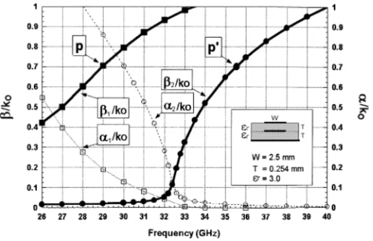
Fig. 2. Normalized phase constants =k (solid line) and the normalized attenuation constants =k (dashed line) against frequency of two-layer broadside-coupled microstrips. The leaky mode (nearly in-phase) and the
leaky mode (nearly out-of-phase) are marked with squares and circles,
respectively.
wider top microstrip can further reduce and to an extremely low value. In this paper, this weakly attenuated mode is purely excited to construct a high-gain narrow-beam leaky-mode antenna.
The remainder of this paper is organized as follows. Section II thoroughly investigates the broadside-coupled transmission line at higher order from the following three perspectives:
1) dispersion characteristics; 2) modal currents;
3) detailed observation of the field distributions.
Section III describes the design procedure of the reported high-gain leaky-mode antenna using broadside-coupled mi-crostrips, as well as the simulated and measured results. Experiments reveal that the reported antenna can control the attenuation rate. Section IV summarizes the results and presents conclusions.
II. CHARACTERISTICS OF TWO-LAYER
BROADSIDE-COUPLEDMICROSTRIPS
The complicated laterally and multiple multilayered transmission lines are reduced to an inhomogeneous broad-side-coupled microstrips structure, as seen in Fig. 1. In this configuration, width, center position, substrate thickness, and substrate dielectric constant for both microstrips are assumed identical for further simplification of the problem. The width of either microstrips is 2.5 mm and the thickness of the substrates with relative dielectric constant of 3.0 is 0.254 mm. The microstrips of infinite length are centered at the -axis. Notice that the substrate thickness of 0.254 mm with low dielectric constant of 3.0 is often the choice for millimeter-wave modules and hybrids.
The full-wave integral-equation method is invoked to obtain two leaky modes at the first higher order , namely, and , spanning the whole -band (26–40 GHz), as shown in Fig. 2. A total of two leaky modes is searched, confirming our expectation that the number of leaky modes should equal that of the microstrips [10].
(a) (b)
(c) (d)
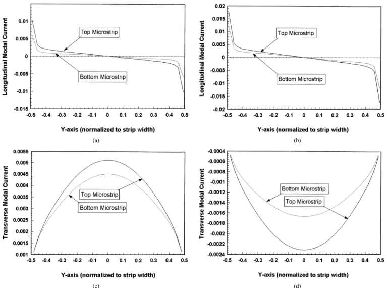
Fig. 3. Modal current distributions of the mode on the top (solid line) and bottom (dashed line) microstrips at 31 GHz. The modal currents flowing on the top and bottom microstrips are nearly in-phase (with a phase difference of 5.4 ) and differ in magnitude by a ratio of 1 : 0.65. (a) The real parts for . (b) The imaginary parts for . (c) The real parts for . (d) The imaginary parts for .
Fig. 2 shows the normalized complex propagation constants
and , where , , and
. is the free-space wavelength. The leaky mode occupies the lower -band. Its cutoff frequency begins around 33.5 GHz where the normalized phase constant crosses unity and the normalized attenuation constant becomes nonzero. The mode spans the higher -band, between 33–40 GHz. Together, and cover the whole -band, representing a bandwidth considerably larger than that of a typical microstrip leaky line at higher order [11]. As shown in Fig. 2, both the distributions of and are much flatter than those of and . The normalized phase constants at point and at , as shown in Fig. 2, are both 0.7, where the normalized attenuation constant (approximately 0.02) is much lower than (approximately 0.19). The value of remains below 0.1 over the frequency range of 32.5–40 GHz, when increases from 0.1 to 1.0, revealing that can establish a wide-band antenna with a great scan range.
Without loss of generality, the modal currents of the and modes at 31 GHz are verified as being of the type, as shown in Figs. 3 and 4, respectively. Both metal strips have
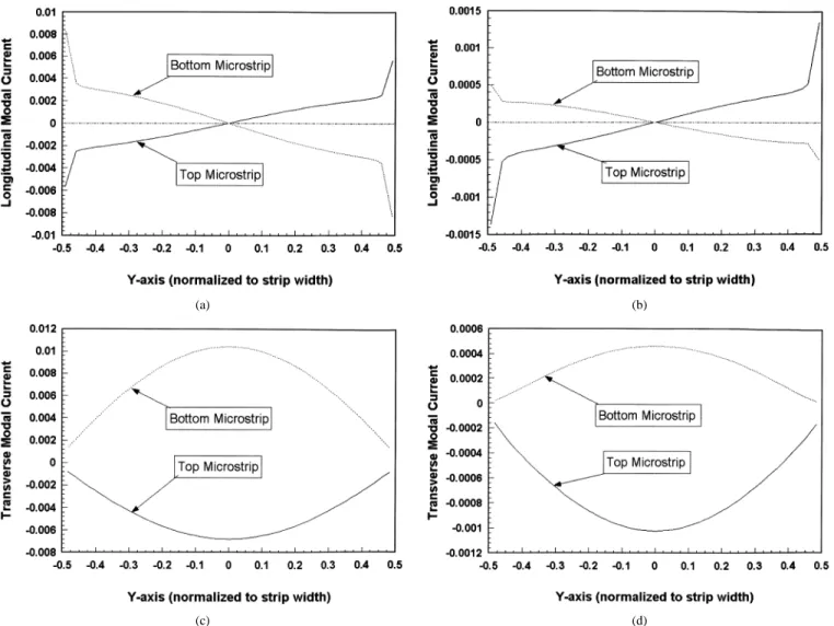
longitudinal (transverse) current distributions that exhibit odd (even) symmetry about the central – -plane. The solid lines in the figures all represent the currents that flow on the top microstrip, and the dashed lines represent those on the bottom microstrip. The modal currents on the top and bottom microstrips are nearly in-phase (with a phase difference of 5.4 ) and out-of-phase (with a phase difference of 186.1 ) for the mode. Notably, the broadside-coupled structure is inhomogeneous and nonsymmetric in the broadside ( -axis); therefore, the and modes can not exhibit either even or odd symmetry. Thus, the modal currents on the top and bottom microstrips differ by 35% and 34% in magnitude for the and modes, respectively. Paralleling to the terminology for bound modes of coupled microstrips, and , the higher order leaky modes, correspond to the and modes, respectively.
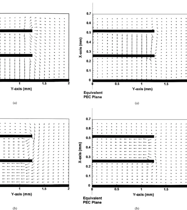
The electric and magnetic fields of the mode at 29 GHz on the transverse plane are plotted in Fig. 5(a) and (b), and the normalized phase constant is 0.70 at this frequency. Similarly, Fig. 6(a) and (b) illustrates the electric and magnetic field of the mode at 34 GHz, where is 0.52. Since the fields due to the modes are antisymmetric against the
(a) (b)
(c) (d)
Fig. 4. Modal current distributions of the mode on the top (solid line) and bottom (dashed line) microstrips at 31 GHz. The modal currents flowing on the top and bottom microstrips are nearly out-of-phase (with a phase difference of 186.1 ) and differ in magnitude by a ratio of 0.66 : 1. (a) The real parts for . (b) The imaginary parts for . (c) The real parts for . (d) The imaginary parts for .
vertical central plane ( – -plane), which is equivalent to a per-fect electric conductor (PEC) plane, only the fields on the right half-plane are shown in Figs. 5 and 6.
Fig. 5(a) indicates that the electric field of the mode concentrates near the edge of the microstrips. The electric-field lines are directed upwardly and downwardly from the top microstrip. Fig. 5(a) and (b) also reveals that the electric and magnetic fields in the sandwiched dielectric layer have smaller amplitudes than those in the bottom dielectric layer because the fields induced by the top and bottom strip oppose and reduce each other. However, the total electric field still points downwards since the magnitude of the current flowing on the top-layer strip is greater than that on the bottom-layer strip. In contrast, the electric fields induced by the two microstrips are equally directed in the bottom dielectric layer, such that the total electric field is their sum and is greater than that in the top dielectric layer.
The electric and magnetic fields of the mode [see Fig. 6(a) and (b)], however, concentrate in the region sandwiched by the two microstrips. The electric fields emanated from the top mi-crostrip terminate on the bottom mimi-crostrip in agreement with the nearly out-of-phase modal currents. Applying the image
theorem [21], we may insert a PEC plane between the two mi-crostrips without changing in the fields. Careful observation on the transverse fields shown in Fig. 6 reveals that the equivalent PEC approaches the top microstrip, which is equivalent to the re-duction of substrate thickness. This is why the dispersion curve of the mode moves to higher frequency than that of the mode.
III. NARROW-BEAMLEAKY-MODEANTENNA
A. Design and Measurement
As stated in Section I, the directivity of the leaky-mode antenna is related to the attenuation constant . The antenna beamwidth falls and the directivity rises as the attenuation constant decreases. Section II showed that a weakly attenuated leaky mode, i.e., , can exist in the two-layer broadside-cou-pled microstrips. Thus, high-gain leaky-mode antennas can be realized with the mode due to the reduction in .
Experiments are carried out for obtaining the radiation characteristics of the conventional isolated microstrip and the two-layer broadside-coupled microstrips. Firstly, an isolated single-layer microstrip is fabricated as a control experiment.
(a)
(b)
Fig. 5. Transversal: (a) electricE-field and (b) magnetic H-field distributions of the leaky mode (approximately in-phase); strong field distribution underneath the bottom microstrip suggests the near in-phase modal current distributions for top and bottom microstrips.
A 50-mm-long microstrip of width 2.5 mm is placed on the 0.254-mm (10-mil)-thick Duroid substrate with relative dielectric constant of 3.0. The feeding network consists of a microstrip power divider, followed by two paths made of a 1/4 and 3/4 lines of appropriate characteristics impedance [22]. The phase difference of the two paths results in 180 out-of-phase at the differential inputs of the leaky line. Thus, the mode (isolated microstrip with substrate thickness of
0.254 mm), , is properly excited.
One additional dielectric layer of the same thickness and and a metal strip with the same width are stacked vertically on the isolated microstrip. However, both the top and bottom strips’ lengths are greatly extended to be 120 mm since is reduced after coupling. Care must be exercised to excite the mode of Fig. 2. As mentioned in Section I, the two-layer broadside-coupled microstrips shown in Fig. 1 can be considered as the
(a)
(b)
Fig. 6. Transversal: (a) electric and (b) magnetic field distributions of the leaky mode (approximately out-of-phase).
simplest three-element Yagi–Uda-like array antenna, including a driver (the bottom microstrip), reflector (the ground plane), and director (the top microstrip). The space distance between the top and bottom microstrips (approximately 0.05 ), however, is much smaller than (the regular value between the first reflector and the driver elements of a typical Yagi–Uda antenna array). Consequently, the coupling between the microstrips is much stronger and both of the nearly in-phase and out-of-phase modes could be excited simultaneously by exciting the bottom microstrip only. Applying the well-known even–odd mode analysis, the power ratio of 0.1–0.9 between the and modes can be obtained. That is, only 10% of the input energy is transferred into the mode, which is bound in the operating frequency band of the mode, and the power of the mode is wasted. In order to reduce the power loss and focus only on the interested mode, the designed antenna is directly fed on both microstrips.
(a)
(b)
Fig. 8. Simulated modal currents flowing on the: (a) top and (b) bottom microstrip of the reported leaky-wave antenna.
Fig. 7 shows the layout graph of this two-layer structure. A 50- transmission line is power divided into two paths abiding the power ration of to excite only the mode. The first path is again evenly power divided into two paths of 180 phase difference to excite the bottom microstrip. The second path, while properly designed to support differential inputs at the top microstrip, is further delayed by 186.1 .
Fig. 8 displays the simulation results of the modal currents that flow on the top and bottom microstrips at 35 GHz from the three-dimensional (3-D) commercial software, HFSS of Ansoft. The arrow points to the direction of the current flow and the length of the arrow is directly proportional to the magnitude of the current. Fig. 8 shows only the first 20 mm (approximately 1.5 ) since the leaky-mode antenna is a traveling-wave an-tenna and the modal currents are distributed periodically along the metal strip, excepting the energy decays exponentially. The distributions of longitudinal (transverse) currents that flow on the two microstrips are both oddly (evenly) symmetric about the plane, showing that the first higher order leaky mode is well excited. The currents that flow on the two microstrips are in opposite directions and the magnitude of the current on the bottom microstrip exceeds that on the top mi-crostrip, establishing that the mode dominates according to the designed feeding network.
The waves that propagate along the transmission line can be extracted from the modal current distributions in Fig. 8 by invoking the matrix-pencil technique [23]. Four modes, two for-ward traveling waves , and their corresponding backward traveling waves , contribute much to the total field, while
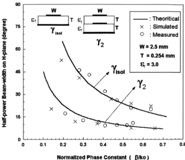
Fig. 9. Theoretical, simulated, and measured half-power beamwidth against normalized phase constants =k for the leaky-wave antenna applying two-layer broadside-coupled microstrips and the isolated leaky microstrip.
the other modes, such as the bound modes and surface-wave leaky modes, are relatively small in magnitude and are neg-ligible under the excitation. The power ratio of to is 1 : 0.11, showing that the designed antenna can radiate around 89% of the energy into space, of which the value is close to the required 90%, as stated in Section I. If the antenna is longer, the amount of falls, while the aperture efficiency gets a little worse [14]. The normalized phase constants of and are 1.04 and 0.67, agreeing closely with the results displayed in Fig. 2. The energy carried by is found to be only 0.98% of that carried by ; hence, the mode is shown to be dominant in the reported leaky-mode antenna.
Fig. 9 presents the theoretical (full-wave integral-equation method), simulated (HFSS, Ansoft) and measured radiation results. The half-power beamwidth on the -plane (elevation plane or – -plane) is plotted against the normalized phase constant to fairly elucidate the gain-enhancement effect. The solid line represents the theoretical result [referring to (1)] and reveals that decreases as increases. The ’s represent the simulated results and the circles represent the measured results. These three results agree closely with each other. Comparing the results for the mode with those for the mode reveals a significant reduction in . The half-power beamwidth of the mode is only approximately
40% of that of the mode over .
B. Control of the Attenuation Rate
As mentioned above, a reduction in the attenuation constant can support a high-gain narrow-beam leaky-mode antenna. It is pointed out in [14] that the decline in and beamwidth can be related to a thin substrate or one with a low dielectric constant. Finely tuning the thickness or dielectric constant of substrates, however, is difficult, as the microwave substrates are usually made according to commercial specifications. The sub-strates with quite a thin thickness or low dielectric constant are typically very fragile and expensive. This section shows that the
Fig. 10. Normalized attenuation constants =k against normalized phase constants =k of the mode due to the variation on W (width of the top microstrip).
attenuation constant can easily be reduced dramatically by controlling the width of the top microstrip.
Fig. 10 presents the normalized attenuation constant of the mode (the mode with approximately out-of-phase modal currents) for various (width of the top microstrip) versus the normalized phase constant . The solid line in Fig. 10 rep-resents the case of and shows that decreases as increases. When the width of the top microstrip is in-creased by 10%, is lower at a given , as illustrated by the dashed line in Fig. 10. Restated, the radiation beamwidth can be reduced by adjusting the width of the top microstrip according to (1).
A leaky-mode antenna that employs two-layer broad-side-coupled microstrips with a wider top microstrip are designed and measured to demonstrate a further reduction of the beamwidth. The feeding network should be carefully designed to excite the mode. The theoretical value (using a two-dimensional (2-D) full-wave integral-equation method) of the normalized attenuation constant at 34 GHz is found to be 0.0043, where is 0.44 and is 5.1 mm. The antenna length is 300 mm (58 at 34 GHz), exceeding 217 mm to radiate above 90% of its power. Fig. 11 depicts the measured radiation pattern along the entire elevation plane ( -plane, ) from 90 to 90 (from the broadside) at 34 GHz. Clearly, since the proposed antenna is long enough to radiate almost all the input energy, no observable back lobe is found in this figure. The measured (angle of the radiation main beam) is 25.2 , agreeing very closely with the theoretical
value 26.1 of obtained from . The
measured half-power beamwidth is 2.1 at , also agreeing closely with the theoretical value 1.5 from (1) and much narrower than that of the leaky-mode antenna with
equal microstrips ( at ). The result
follows the expectation from Fig. 10. An overall efficiency of 81% is measured for the leaky-mode antenna prototype.
Fig. 11. Measured far-field radiation pattern in the elevation plane (x–z-plane) cut of the reported leaky-mode antenna with a wider top microstrip (W =
2:75 mm, W = 2:5 mm).
The energy loss mainly comes from the mismatching loss and material losses (conductor loss plus dielectric loss). The return loss is measured to be lower than 15 dB from 32 to 36 GHz showing a bandwidth of 11.8%. However, the material losses are difficult to measure from experiment; hence, only simula-tion results are mensimula-tioned as budget analyses. The conductor (dielectric) loss of the reported electrically long antenna is established to be 8.4% (3.6%), which is the difference between the cases of ideal and actual conductivity (loss tangent). Several measurements show that this antenna can scan from 20 to 40 with below 5 , establishing that this leaky-mode antenna can scan a very wide range.
IV. CONCLUSION
The higher order leaky modes of broadside-coupled line structures are investigated. Two-layer broadside-coupled mi-crostrip structures are considered, and the dispersion curves, modal currents, and electromagnetic fields are comprehensively discussed. The leaky region of this structure is much broader than that of a conventional isolated microstrip. The coupled mode with approximately in-phase modal currents always falls into a lower frequency band and should be treated carefully in practical multilayered microwave integrated circuits (MICs) or monolithic microwave integrated circuits (MMICs).
This paper offers a practical design example of a leaky-mode antenna that invokes the coupled mode with approxi-mately out-of-phase modal currents. This weakly attenuated mode can be primarily excited to fabricate a high-gain narrow-beam leaky-mode antenna. However, the attenuation rate can also be increased or decreased over a very wide range by adjusting the ratio of the strips’ widths, showing a plain approach to a highly directed antenna, which is important to modern wireless communication systems.
REFERENCES
[1] J. E. Dalley, “A strip-line directional coupler utilizing a nonhomoge-neous dielectric medium,” IEEE Trans. Microwave Theory Tech., vol. MTT-17, pp. 706–712, Sept. 1969.
crostrip,” IEEE Trans. Microwave Theory Tech., vol. 40, pp. 58–66, Jan. 1992.
[8] F. J. Villegas, D. R. Jackson, J. T. Williams, and A. A. Oliner, “Leakage fields from planar semi-infinite transmission lines,” IEEE Trans.
Mi-crowave Theory Tech., vol. 47, pp. 443–454, Apr. 1999.
[9] K.-F. Huang and C.-K. C. Tzuang, “Leaky modes of vertically stacked microstrips at higher order,” in IEEE MTT-S Int. Microwave Symp. Dig., vol. 2, June 2000, Paper WEIF-5, pp. 1077–1080.
[10] C.-N. Hu and C.-K. C. Tzuang, “Analysis and design of large leaky-mode array employing the coupled-mode approach,” IEEE Trans.
Microwave Theory Tech., vol. 49, pp. 629–636, Apr. 2001.
[11] A. A. Oliner and K. S. Lee, “The nature of the leakage from higher modes on microstrip line,” in IEEE MTT-S Int. Microwave Symp. Dig., 1986, pp. 55–60.
[12] W. Menzel, “A new traveling-wave antenna in microstrip,” Arch. Elektr.
Ubertragung, vol. 33, pp. 137–140, Apr. 1979.
[13] Y. Qian, B. C. C. Chang, M. F. Chang, and T. Itoh, “Multi-mode mi-crostrip antennas for reconfigurable aperture,” in IEEE AP-S Symp. Dig., vol. 1, 2000, pp. 318–320.
[14] K. S. Lee, “Microstrip line leaky-wave antenna,” Ph.D. dissertation, Polytech. Inst., Brooklyn, NY, 1986.
[15] D. R. Jackson and A. A. Oliner, “A leaky-wave analysis of the high-gain printed antenna configuration,” IEEE Trans. Antennas Propagat., vol. 36, pp. 905–910, July 1988.
[16] D. R. Jackson, A. A. Oliner, and A. Ip, “Leaky-wave propagation and radiation for a narrow-beam multiple-layer dielectric structure,” IEEE
Trans. Antennas Propagat., vol. 41, pp. 344–348, Mar. 1993.
[17] C.-Y. Lee, A. Basu, J. Liao, J. S.-M. Wong, B. Houshmand, and T. Itoh, “Millimeter-wave dielectric leaky-wave antennas,” in Int. Signals,
Sys-tems and Electronics Symp., 1995, pp. 21–24.
[18] Y. Wagatsuma, Y. Daicho, and T. Yoneyama, “Millimeter-wave planar antenna for car warning radar,” in Millimeter Waves Topical Symp., July 1997, pp. 173–176.
from the National Chiao Tung University, Hsinchu, Taiwan, R.O.C., in 1997 and 1999, respectively, and is currently working toward the Ph.D. degree at the National Chiao Tung University.
His current research interests include electromag-netic-field theory analysis and its application on designing leaky-mode antennas.
Ching-Kuang C. Tzuang (S’80–M’80–SM’92–
F’99) received the B.S. degree in electronic engi-neering from the National Chiao Tung University, Hsinchu, Taiwan, R.O.C., in 1977, the M.S. degree from the University of California at Los Angeles, in 1980, and the Ph.D. degree in electrical engineering from the University of Texas at Austin, in 1986.
From 1981 to 1984, he was with TRW, Redondo Beach, CA, where he was involved with analog and digital MMICs. Since 1986, he has been with the Institute of Communication Engineering, National Chiao Tung University. His research activities involve the design and development of millimeter-wave and microwave active and passive circuits and the field theory analysis and design of various complex waveguiding structures and large-array antennas. He has supervised 58 M.S. students and 15 Ph.D. students.
Dr. Tzuang helped in the formation of the IEEE Microwave Theory and Techniques Society (IEEE MTT-S) Taipei chapter, and served as secretary, vice chairman, and chairman in 1988, 1989, and 1990, respectively. He has been on the Asia–Pacific Microwave Conference International Steering Committee, where, since 1994, he has represented the Taipei chapter as the international liaison officer.