突起缺陷及應力對新型矽氧氮SiOxNy薄膜用於有機發光二極體之水氣阻障探討
101
0
0
全文
(2) 突起缺陷及應力對新型矽氧氮SiO x N y 薄膜用於有機發光二極體之水氣阻障探討. The Effects of Hillock Defect and Stress on the Moisture Resistance of Novel SiOxNy Passivation Layer for OLED Applications. Student:Yi-Jen Chen Advisor:Dr. Jihperng (Jim) Leu. 研 究 生:陳怡臻 指導教授:呂志鵬. 國 立 交 通 大 學 材 料 科 學 與 工 程 學 系 碩 士 論 文. A Thesis Submitted to Department of Materials Science and Engineering College of Engineering National Chiao Tung University in partial Fulfillment of the Requirements for the Degree of Master in Materials Science and Engineering June 2008 Hsinchu, Taiwan, Republic of China. 中華民國九十七年六月.
(3) 突起缺陷及應力對新型矽氧氮SiOxNy薄膜用於有機發光二極體之水氣阻障探討 學生:陳怡臻. 指導教授:呂志鵬 博士. 國立交通大學材料與工程學系碩士班. 摘要. 有機發光二極體(OLED)顯示器因其擁有自體發光之能力而不需背向光源 之調節,以及快速的反應時間(<10 ms)、廣視角(170°以上)、色彩逼真、優 良的對比與亮度、低操作電壓(3-10 V)以及省電等優點,故在過去幾年快速成 長。然而,其有機物及電極對水氣及氧氣非常敏感,在無保護的情況下,水氣 及氧氣會迅速降低OLED元件的性能。在此現況下,本研究動機在尋找低成本、 製程簡單且高可靠性,用於OLED的氮氧化物或氮化物基底(oxynitride or nitride ) 之 薄 膜 阻 障 層 。 我 們 利 用 一 套 新 穎 的 蒸 鍍 系 統 (Ar ion beam evaporation technique)進行薄膜沉積,首先探討氮氧化矽阻障層之成分組 成、微觀結構及表面形貌,並且改變其基材溫度及氣體流速來探討其SiOxNy/Al 薄膜的表面形貌及薄膜應力之影響。此外,並調查水氣阻障與薄膜缺陷(突起缺 陷及Al晶界)之關係。最後,探討突起密度以及其高度對於水氣阻障能力之影響。 從實驗的結果發現氮氧化矽薄膜呈現非晶結構,其 Si: O: N 成分比例為 1: 2: 0.67。鋁薄膜呈現柱狀結構,其晶粒分布介於 50 到 100 奈米。吾人發現, Al 突起缺陷是造成阻障層高水氣穿透的主要原因,同時並提出一套突起密度及 其高度的可能機制。突起密度和鋁晶粒大小有關,而凸起高度和薄膜應力有正向 關係。在高基材溫度、高氣體流速的情況下,其突起缺陷密度會較少但是其高度 會較高;在低基材溫度、低氣體流速的情況下,其突起缺陷密度會較多但是其高 I.
(4) 度會較低。因此,如果使用一層阻障層的情況下,高溫高流速的阻氣能力會較低 溫低流速的來的佳。但是,如果以層數為考量的話,低溫低流速因其缺限高度較 低,所以只需要較少之阻障層數即可把缺陷完全癒合而高溫高流速則需較多的層 數。總結來說,藉由改變鍍膜參數(氣體流量及基材溫度)來控制突起缺陷的形 成,對於阻障層的阻氣能力有絕對的關係。. II.
(5) The Effects of Hillock Defect and Stress on the Moisture Resistance of Novel SiOxNy Passivation Layer for OLED Applications. Student: Yi-Jen Chen. Advisor: Dr. Jihperng (Jim) Leu. Department of Materials Science and Engineering National Chiao Tung University. Abstract. Organic light-emitting-diode displays (OLED) have gained momentum in the past few years because it was an emissive system creating its own light rather than relying on modulating a backlight. In addition, OLED possessed fast response time (<10ms, 100 times faster than TFT-LCD), wide view angle (>170°), true colors, excellent contrast ratio, brightness, low operating voltage and potentially less power consumption.. However, its broad adoption has been hindered by the sensitivity of. organic and electrode to the moisture and oxygen, which can quickly degrade the device performance if not properly protected. This motivated us to explore a simple, cheap, but reliable oxynitride-based thin film barrier for OLED in this study. The composition, microstructure and morphology of SiOxNy barrier layers deposited by a modified Ar ion beam evaporation system were first investigated. Then, the effects of substrate temperatures (60-90 oC) and gas flow rates (300-480 sccm) on the morphology and stress of SiOxNy/Al stack were examined. In addition, the roles of defects such as hillocks and grain sizes of Al films was studied and correlated with the moisture resistance of SiOxNy barrier films. Finally, the moisture barrier performance in terms of hillock density and hillock height was further discussed if multiple-layered. III.
(6) passivation was warranted. In this study, SiOxNy layers were amorphous and the composition of Si: O: N was in the ratio of 1: 2: 0.67. Al films exhibited columnar structure with grain size distribution 50 to 100 nm after the deposition of SiOxNy. Al hillock was found to be the culprit of high moisture permeation in the passivation layer. A model of hillock formation in SiOxNy/Al was proposed in this thesis to illustrate the causes for their difference in hillock density and height. The hillock density was related to the initial Al grain size, while the hillock height was primarily derived by SiOxNy stress. The tallest height of hillock affected greatly on the numbers of barrier layers for complete sealing of defects. Therefore, high substrate temperature and high N2 gas flow rate deposition process yielded barrier films with less hillocks and improved moisture resistance if single layer of passivation was employed, while lower deposition temperature and low N2 gas flow rate were preferred for least number of layers if multiple-layer structure was adopted. In summary, defect control of Al hillocks was essential for controlling the moisture barrier performance in the practical OLED stack.. IV.
(7) Acknowledgements 得以完成本論文,首先感謝呂志鵬老師兩年來細心且認真的指導,除了研究 上的幫助外,老師亦不吝於與學生分享休閒興趣,帶領我們參與馬拉松 ing、一 探司馬庫斯之美等,在此向老師致上最誠摯的謝意。感謝交通大學張立教授、潘 扶民教授及許鉦宗教授於口試期間,細心且親切的指正本論文疏失缺漏之處,並 提供許多寶貴意見,使本論文更加完整。 在兩年的研究生活中,由衷的感謝徐國原學長不厭其煩的與我討論研究內容 與問題,由於學長的幫助,使本論文能順利完成。感謝 NIP 實驗室的夥伴們,牧 龍學長、昱涵學長、明義學長、幸玲學姊、泰印學長、弘恩學長、欣源學長、鈞 元學長、季高學長、冠宇學長、王智同學與少農同學的照顧與指點,尉霖學長的 TEM 相助,以及尹瀅學妹、茹瑛學妹、詩雅學妹及晉誠學弟的協助與陪伴,使這 兩年的研究生活不再枯燥。感謝我的朋友明慧、靜雯、全雯、文馨等人的陪伴與 包容,在我心情不好的時候,給我鼓勵及安慰。感謝華映的計畫贊助,得以讓論 文能順利完成。 最後,由衷的感謝我的家人及男朋友博傑,在我背後無條件的支持與關心, 使我能完成這篇論文,在此向他們獻上我最深的感激。. V.
(8) Contents 摘要................................................................................................................................ I Abstract ........................................................................................................................III Acknowledgements....................................................................................................... V Contents .......................................................................................................................VI List of Tables............................................................................................................. VIII List of Figures ..............................................................................................................IX Chapter 1 Introduction ...................................................................................................1 1.1 Background ......................................................................................................1 1.2 Overview..........................................................................................................3 Chapter 2 Literature Review..........................................................................................4 2.1 Introduction of OLED......................................................................................4 2.1.1 Mechanisms of Degradation .................................................................5 2.1.2 Requirements of WVTR and OTR........................................................7 2.1.3 Methods for Measuring WVTR ............................................................8 2.2 Passivation and Packaging Technologies in OLED Devices .........................10 2.2.1 Glass Packaging ..................................................................................10 2.2.2 Thin Film Packaging........................................................................... 11 2.3 Microstructure of Thin Films.........................................................................14 2.4 Thin Film Stress .............................................................................................17 Chapter 3 Experimental ...............................................................................................19 3.1 Deposition System .........................................................................................19 3.2 Sample Preparation ........................................................................................21 3.3 Experimental Procedure.................................................................................23 3.4 Characterization Methodologies ....................................................................25 3.4.1 Decoration of Al Hillock Defect by a Selective Etching Process.......25 3.4.2 Ca Button Test for Moisture Permeation ............................................27 3.5 Instrumentation and Data Analysis ................................................................28 3.5.1 FE-SEM ..............................................................................................28 3.5.2 HR-TEM .............................................................................................28 3.5.3 X-ray Diffraction (XRD) ....................................................................28 3.5.4 Atomic Force Microscope (AFM) ......................................................29 3.5.5 Nanoindentation..................................................................................29 3.5.6 Specular Reflectance Fourier-Transform Infrared Spectroscopy (Specular Reflectance FT-IR) ......................................................................31 3.5.7 X-ray Photoelectron Spectroscopy (XPS) ..........................................32 VI.
(9) 3.5.8 Bending beam system .........................................................................33 3.5.8.1 Evolution of Stoney’s Equation ...............................................33 3.5.8.2 Bending Beam System.............................................................34 3.6 Grain Size Analysis of Al by IMAGE J .........................................................38 Chapter 4 Results and Discussion................................................................................42 4.1 Chemical Structure and Composition Analysis of SiOxNy Layers.................42 4.1.1 Analysis by Specular Reflectance FTIR Spectroscopy.......................42 4.1.2 Composition Analysis by XPS............................................................43 4.2 Morphology and Microstructure of Barrier Layers/Al Samples....................45 4.3 Hillock Formation..........................................................................................48 4.3.1 Hillock Density ...................................................................................48 4.3.2 Hillock Height.....................................................................................50 4.4 Correlation between Moisture Resistance and Hillock Formation ................53 4.5 Al Grain Size..................................................................................................54 4.6 Stress Analysis ...............................................................................................63 4.6.1 Young’s Modulus of Substrates...........................................................63 4.6.2 As-deposited stress in thin film Al, SiOxNy/Al and SiOxNy................64 4.6.3 Stress during Thermal Cycle...............................................................67 4.7 Discussion ......................................................................................................70 4.7.1 Microstructure and Moisture of Barrier Layer....................................70 4.7.2 Hillock Formation...............................................................................71 4.7.2.1 Mechanisms of Hillock Formation ..........................................71 4.7.2.2 Defects Caused by Stress .........................................................75 4.7.2.3 Suppression of Hillocking........................................................76 4.7.3 Hillock Density vs. Grain Boundary...................................................77 4.7.4 Hillock Height vs. Stress.....................................................................77 4.7.5 Model of Hillock Formation in SiOxNy/Al/glass for OLED Applications .................................................................................................78 Chapter 5 Conclusions .................................................................................................82 References....................................................................................................................84. VII.
(10) List of Tables Table 2.1 Summary of WVTR measuring methods, their detection principles and advantages and disadvantages..............................................................................9 Table 2.2 Some reported water vapor resistance properties of passivation layers.......12 Table 3.1 Deposition parameters of SiOxNy barrier layer. ...........................................22 Table 3.2 Description of wet etching SiO2 layer. [47] .................................................26 Table 3.3 Description of wet etching Si3N4 layer. [47]................................................27 Table 3.4 Description of wet etching Al layer. [47] .....................................................27 Table 4.1 Si-O absorption peak position of three types of passivation layer. ..............42 Table 4.2 Binding energies and composition quantification of oxynitride film deposited under 80 ℃ and low flow rate condition. ..........................................45 Table 4.3 Binding energies and composition quantification of oxynitride film deposited under 80 ℃ and high flow rate condition..........................................45 Table 4.4 EDS analysis of the defect shown in Fig. 4.5 (a). ........................................47 Table 4.5 Al hillock density of the SiOxNy/Al films deposited under different flow rate condition at various substrate temperatures.........................................................48 Table 4.6 The maximum height of hillock of the SiOxNy/Al films deposited under different flow rate condition at various substrate temperatures...........................50 Table 4.7 The crystallite sizes of Al in SiOxNy/Al/Alq3/glass sample stack, where SiOxNy was deposited under different flow rate condition at various substrate temperatures.........................................................................................................59 Table 4.8 As-deposited stress of 50 nm SiOxNy/200 nm Al for SiOxNy films deposited under different flow rate conditions at various substrate temperatures. ..............67 Table 4.9 The as-deposited stress of SiOxNy films deposited under different flow rate conditions and various substrate temperatures. ...................................................67 Table 4.10 Hillock density of the sample and the corresponding Al grain size...........77 Table 4.11 As-deposited stress of the multilayer and the corresponding hillock height. ..............................................................................................................................78. VIII.
(11) List of Figures Figure 2.1 The film stack and structure of OLED device..............................................4 Figure 2.2 Scheme of (1) Trans-Complexation of 8-Hq with Water in the Alq3 Complex and (2) Oxidative Polymerization of 8-Hq. [15] ..................................5 Figure 2.3(a) Mechanism of dark spots formation during operation under water vapor environment. (b) Mechanism of dark spots formation for an unbiased device under a pure oxygen atmosphere. [17].................................................................7 Figure 2.4 Requirements of WVTR and OTR for different applications. [19]..............8 Figure 2.5(a) Illustration of the structure for Ca test before testing, (b) the structure changed after H2O permeating...........................................................................10 Figure 2.6 Schematic diagram of glass package in OLED technology........................ 11 Figure 2.7 Schematic diagram of thin-film barrier package in OLED technology......13 Figure 2.8 Organic/inorganic multi-layer structure from Vitex Systems. (Reproduced courtesy of Vitex Systems.)[7, 8].......................................................................14 Figure 2.9 The deposition process of BarrixTM layers. [7, 8].......................................14 Figure 2.10 Schematic diagram illustrating fundamental growth processes. The growth of thin films progresses through consecutive stages: stage1 is nucleation, stage 2 is island growth, stage 3 is coalescence of islands, stage 4 is formation of polycrystalline islands and channels, and stage 5 is development of continuous structure and thickness growth. [39] ...............................................15 Figure 2.11 Structural zones in PVD films as a function of substrate temperature and chamber pressure. [9].........................................................................................17 Figure 3.1 The schematic diagram of an argon ion-beam evaporation system. (Courtesy of China Picture Tube, Inc.) ..............................................................20 Figure 3.2 Energy distributions of the particle arriving to the substrate surface for conventional sputtering system and Ar ion beam evaporation system. (Courtesy of China Picture Tube, Inc.)...............................................................................21 Figure 3.3 The film thickness and stack structure of samples. ....................................22 Figure 3.4 Flow-chart of experimental procedures......................................................24 Figure 3.5 Schematic diagrams of etching process for decoration of Al hillocks. ......26 Figure 3.6 XRD patterns of crystalline film with finite crystallite size. [48] ..............29 Figure 3.7 Load-Displacement of Nanoindentation. [49] ............................................31 Figure 3.8 Schematic diagram of a specular reflectance infrared spectroscopy. .........32 Figure 3.9 Schematic setup of a bending beam system for stress measurement. ........36 Figure 3.10 Schematic diagram of the laser routes in the bending beam system. .......37 Figure 3.11 SEM image which has been demarcated the grain area. ..........................38 Figure 3.12 Illustration of altering interactively the brightness and contrast of the IX.
(12) image to be relative block and white. ................................................................39 Figure 3.13 Location of the command “Analyze Particles”. .......................................40 Figure 3.14 Analysis result of grain size distribution. .................................................41 Figure 4.1 Specular reflectance FTIR spectrum of three types of passivation layer: (1) pure SiO2, (2) SiOxNy under high nitrogen flow rate, and (3) SiOxNy under low nitrogen flow rate...............................................................................................43 Figure 4.2 The XPS Si 2p, N 1s, and O1s spectra of oxynitride films deposited under 80 ℃ (a) low flow rate and (b) high flow rate conditions. The references of Si 2p signals: Si-Si (99.4 eV), Si-N (101.9 eV), and Si-O (103.4 eV). [58]..........44 Figure 4.3 SEM top-view graphs of the SiOxNy films deposited at substrate temperatures 90℃: (a) under high flow rate, (b) under low flow rate...............46 Figure 4.4 SEM top-viewgraphs tilted 52º of the SiOxNy films: (a) unknown bump, (b) crack...................................................................................................................47 Figure 4.5 SEM photographs: (a) defects of Al hillock and (b) topography after wet etch of Al hillocks. .............................................................................................47 Figure 4.6 OM photographs magnified 1000x: under low flow rate at various substrate temperatures: (a) 60 ℃, (b) 80℃, and (c) 90℃ and under high flow rate at various substrate temperatures: (d) 60 ℃, (e) 80℃, and (f) 90℃....................49 Figure 4.7 AFM 2D images (2μm×2μm): (a) substrate temperature is 90℃ under high flow rate, (b) substrate temperature is 90℃ under low flow rate, (c) substrate temperature is 80℃ under high flow rate, (d) substrate temperature is 80℃ under low flow rate, (e) substrate temperature is 60℃ under high flow rate, and (f) substrate temperature is 60℃ under low flow rate. .....................................52 Figure 4.8 Calcium button test of SiNxOy barrier films deposited under (a) high flow rate and (b) low flow rate...................................................................................53 Figure 4.9 X-ray diffraction pattern of SiOxNy/Al/Alq3/glass sample, where SiOxNy was deposited under high flow rate at various substrate temperatures..............57 Figure 4.10 X-ray diffraction pattern of SiOxNy/Al/Alq3/glass, where SiOxNy was deposited under low flow rate at various substrate temperatures. .....................58 Figure 4.11 SEM top-view graphs of the SiOxNy films deposited under high flow rate at various substrate temperatures: (a) 90 ℃, (b) 80℃, and (c) 60℃ and under low flow rate at various substrate temperatures: (d) 90 ℃, (e) 80℃, and (f) 60 ℃........................................................................................................................60 Figure 4.12 Cross-sectional TEM photograph of SiOxNy/Al/Alq3/glass stack for SiOxNy films prepared at high flow rate and substrate temperature 60℃ condition. ...........................................................................................................61 Figure 4.13 Al grain size distributions obtained fromSEM image: (a) SiOxNy films deposited under 60℃ and two different gas flow rate conditions. (b) films X.
(13) deposited under 80℃ and two gas flow rate conditions. (c) films deposited under 90℃ and two gas flow rate conditions. (d) films deposited under different substrate temperature and high flow rate conditions...........................63 Figure 4.14 Modulus vs. displacement of the glass substrate......................................64 Figure 4.15 Stress vs. annealing temperature of 200 nm Al films. ..............................66 Figure 4.16 Stress vs. annealing temperature of 50nm SiOxNy/200 nm Al films with different SiOxNy deposition conditions: (a) △ stood for the SiOxNy film which was deposited under low gas flow rate and 60℃. ◇ stood for the SiOxNy film which was deposited under high gas flow rate and 60℃. (b) △ stood for the SiOxNy film which was deposited under low gas flow rate and 80℃. ◇ stood for the SiOxNy film which was deposited under high gas flow rate and 80℃...70 Figure 4.17 SEM top-view graphs of the SiOxNy films after 200℃ thermal cycle: (a) films deposited under 60℃ (b) films deposited under 80℃.............................70 Figure 4.18 Schematic diagrams of two models correlating to the hillock formation behavior on Al thin films. [69] ..........................................................................73 Figure 4.19 Schematic diagrams of hillock formation comparing a film with small grains to a film with large grains. [69]...............................................................74 Figure 4.20 Illustration of thin film failure by the thin film stress. [10]......................76 Figure 4.21 The model of hillock formation: (a) sample prepared under the same deposition conditions of Al films (b) barrier films deposited under low temperature caused less Al grain growth with lowest stress, shortest hillock height and highest hillock density (c) barrier films deposited under high temperature caused more Al grain growth with largest stress, tallest hillock height and lowest hillock density.......................................................................81. XI.
(14) Chapter 1 Introduction 1.1 Background Organic light emitting devices (OLED) have gained momentum in flat-panel display in the past few years for its fast response time (<10ms), wide view angle (>170°), low operating voltage (3-10 V), excellent contrast and brightness compared to those of LCD-TFT or LED. [1] However, their device performance degraded drastically by permeated moisture and O2 through the oxidation of the cathode and/or active OLED polymers. [2, 3] The conventional encapsulation package of the OLEDs by metal or glass lid to prevent gas permeation has been widely used with excellent result with built-in desecrator. [4] However, the weight issue and high cost associated with difficult manufacturing processes, such as the permeation of oxygen and moisture through the glue, the impossible application to flexible display using polymer substrate, and the difficulty of large area application restricted the use of metal or glass lid in the flexible OLED displays. [4] Therefore, thin film package for FOLED’s application was necessitated to prevent the permeation of water vapor and oxygen practically for long service time. Although inorganic thin films like oxide- or nitride- based have been studied as barrier layers for oxygen and water vapor, these researches still showed too high water vapor transmission rate (WVTR) and oxygen transmission rate (OTR) to apply to display industries. [5, 6] Moreover, the permeation mechanism of water vapor has not been well known yet. In general, WVTR should be lower than 10-6 g/m2-day and OTR should be lower than 10-5 g/m2-day in OLED’s applications. Recently, BarrixTM, comprised of alternating layers of polymer and ceramic film deposited in vacuum to about 3 μm, was announced by Vitex System (USA) that BarrixTM layers can achieve the requirements of WVTR for OLED’s applications. [7, 8] However, the cost and 1.
(15) thermo-mechanical integrity of such ceramic/polymer multiple-layer structure (BarrixTM layer) remained a lingering problem. For OLED passivation and packaging, the deposition temperature cannot exceed 100 ℃ in order not to degrade OLED’s small molecules or polymers. However, low substrate-temperature was expected to greatly affect the microstructure, morphology (pinhole) and even the stress of barrier films because of its low atomic surface mobility and diffusion. [9] Besides, plasma damage during the passivation layer deposition shall be avoided if films deposited by sputtering or plasma-enhanced chemical vapor deposition (PECVD). Hence, evaporation techniques were often employed. But, conventional thermal evaporation often produced films with loose microstructure due to the low atom mobility. As a result, a modified Ar ion beam evaporation technique [46] was employed in this study for the deposition of light-emitting organic, Alq3, aluminum film as cathode and moisture barrier layer for its high deposition rate and reasonable particle energy (~25 eV) reaching the surface of substrate. More importantly, the objective of this study was to develop reliable inorganic oxynitride- barrier films with low moisture permeability for the hermetic sealing of OLED packaging using a silicon oxynitride/Al/Alq3/glass multiple-layered structure. Specifically, the composition, microstructure and morphology of barrier were investigated. Then, the effects of substrate temperature and gas flow rates on the morphology and residual stress of SiOxNy onto Al electrode were first studied. Then, the roles of defects such as hillocks and grain sizes of Al films associated with the water permeation in inorganic barrier films were investigated and discussed. Finally, the moisture barrier performance in terms of hillock density and hillock height was further discussed if multiple-layered passivation is warranted.. 2.
(16) 1.2 Overview This thesis was organized into five chapters. Following a concise introduction in Chapter 1, Chapter 2 reviewed the OLED package, the mechanisms of OLED device degradation, methodologies for measuring water vapor transmission rate (WVTR), and microstructure of thin films deposited at various temperature and pressures. Chapter 3 described the modified Ar ion beam evaporation system, sample preparation, experimental procedures, instrumentation and methodologies for characterizing the composition of SiOxNy passivation layer, Al hillock, its density, and height, and the thermal stress of SiOxNy/Al. Chapter 4 described key results and discussion. Specifically, the relationship between moisture permeation and defects such as hillock was investigated. The mechanism for the formation of hillocks and the root-causes for different hillock density or hillock height were examined and proposed. Then key results and conclusion of this thesis were summarized in Chapter 5.. 3.
(17) Chapter 2 Literature Review 2.1 Introduction of OLED The next great emerging technology in the display industry was expected to come from organic light-emitting-diode (OLED). [12] A typical OLED device structure was shown in Fig. 2.1, in which organic material such as Alq3 was presented in the form of thin film with a thickness not exceeding the depth of the ink on the paper. OLED have gained momentum in the past few years because it was an emissive system creating its own light rather than relying on modulating a backlight. In addition, OLED possessed fast response time (<10 ms), wide view angle (>170°), true colors, excellent contrast ratio, brightness, low operating voltage (3-10 V) and potentially less power consumption compared to those of LCD or LED. [1] As a result, OLED had the opportunity to replace LED or LCD in display industry. [1] However, its broad adoption has been hindered by several issues; namely (1) poor production yields which makes the product not cost attractive and deter investments and (2) device lifetime and reliability due to its sensitive to moisture and oxygen, which can quickly degrade the device performance and produce the black spots if unprotected. [2, 3]. Figure 2.1 The film stack and structure of OLED device. 4.
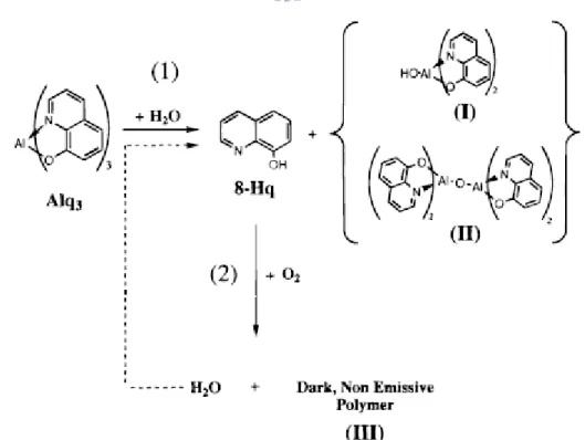
(18) 2.1.1 Mechanisms of Degradation Although organic light-emitting diodes (OLEDs) had many above-mentioned advantages, the short lifetime was still a critical issue to be addressed. Many mechanisms have been proposed and reported for the decay in luminance, ranging from crystallization of the organic molecules,[13, 14] decomposition of Alq3 molecules, [15] delamination at the cathode/Alq3 interface, [13, 16, 17] and electrochemical reactions at the organic/electrode interfaces. [17, 18] H. Aziz et al. [13] proposed the Alq3 molecules became crystalline clusters by exposing to humidity and delamination occurred between cathode/Alq3 interface because the crystalline Alq3 clusters was thicker than the surrounding amorphous regions and lead the cathode/Alq3 contact isolated.. F. Papadimitrakopoulos et al. [15]. suggested a series of probable reaction for the failure of Alq3-based OLEDs as shown in Fig.2.2. Reaction (1) showed water acts as a catalyst to hydrolyze Alq3 to become freed 8-hydroxyquinoline (8-Hq) and then (2) an oxidative condensation reacted with yielding a nonemissive polymeric byproduct.. Figure 2.2 Scheme of (1) Trans-Complexation of 8-Hq with Water in the Alq3 5.
(19) Complex and (2) Oxidative Polymerization of 8-Hq. [15]. M. Schaer et al. [17] presented two different degradation mechanisms under moisture and oxygen environments as shown in Figs.2.3 (a) and (b), respectively. Fig.2.3 (a) showed water vapor entered from the defects, such as cracks, pinholes etc. and diffused to the cathode/organic interface. When the device was working, water was then reduced at the cathode and yielded hydrogen gas. The electrochemical reduction was: 2H 2 O+2e- → H 2 +2OH -. (2.1). Then, the bubbles were formed by the evolving hydrogen gas and the organic/electrode interfaces were separated. In contrast, Fig. 2.3 (b) showed oxygen enters from the defects and diffuses to the cathode/organic interface. As the metal layer was oxidized at the cathode/organic interface, the molecular volume which increased of the oxide led to interface delamination. In summary, organic layers and metal cathodes of OLEDs were sensitive to moisture and oxygen, no matter what mechanism was involved. Therefore, preventing moisture and oxygen permeation in OLED was an immediate solution to extend the life time of devices.. 6.
(20) Figure 2.3(a) Mechanism of dark spots formation during operation under water vapor environment. (b) Mechanism of dark spots formation for an unbiased device under a pure oxygen atmosphere. [17]. 2.1.2 Requirements of WVTR and OTR Fig. 2.4 showed the water vapor transmission rate (WVTR) and oxygen transmission rate (OTR) required for various organic electronic devices. [19] Among these devices ranging from LCD, solar cell to OLED, the requirements for OLED application was most stringent. In general, water vapor transmission rate (WVTR) should be lower than 10-6 g/m2-day and oxygen transmission rate (OTR) should be lower than 10-5 g/m2-day for OLED’s applications. The WVTR requirements for TFTs 7.
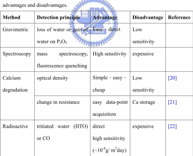
(21) or LCD were not as critical as those for OLEDs. The sensitivity to moisture and oxygen in OLED was much more than 10000 times in LCD. Apparently, oxygen and moisture permeation was a serious issue for developing OLED applications.. Figure 2.4 Requirements of WVTR and OTR for different applications. [19]. 2.1.3 Methods for Measuring WVTR There were many methods for measuring WVTR, which have been developed in the past few years. These methods and their detection principles were listed in Table 2.1, along with their merits and disadvantage. Among these methods, optical calcium degradation test was the most commonly used for flexible OLED’s applications, which was often named as the “Ca test” or “Ca button test”.. This. method was based on the corrosion of calcium films and subjected at a fixed temperature and humility. At the start, the calcium film was a reflecting metallic layer as shown in Fig. 2.5(a). As water and oxygen permeated into metallic calcium, calcium would convert to a transparent oxide or hydroxide salt as shown in Fig. 2.5(b). 8.
(22) The related chemical reactions of calcium with H2O and O2 were assumed to be the following: 2Ca+O2→2CaO,. (2.2). Ca+H2O→CaO+H2,. (2.3). CaO+H2O→Ca(OH)2 .. (2.4). Then, the reacted sites can be observed as spots on the Ca film. Although it did not distinguish between oxygen and water permeation and it was more qualitative comparison, it was still a simple and direct method to compare the permeability of different materials.. Table 2.1 Summary of WVTR measuring methods, their detection principles and advantages and disadvantages. Method. Detection principle. Gravimetric. loss of water or gain of Easy、direct. Low. water on P2O5. sensitivity. mass. expensive. Spectroscopy. Advantage. spectroscopy, High sensitivity. Disadvantage Reference. fluorescence quenching Calcium. optical density. degradation. Simple、easy、 Low cheap. change in resistance. [20]. sensitivity. easy data-point Ca storage. [21]. acquisition Radioactive. tritiated water (HTO) direct or CO. high sensitivity (~10-8g/ m2day). 9. expensive. [22].
(23) barrier Ca glass (a). H2O. H2O. H2O. barrier Ca glass (b) Figure 2.5(a) Illustration of the structure for Ca test before testing, (b) the structure changed after H2O permeating.. 2.2 Passivation and Packaging Technologies in OLED Devices 2.2.1 Glass Packaging To protect the OLED’s organic thin film materials and cathode metal from the oxidation or reaction, display manufacturers first employed glass as substrate and then glue a metal can or glass lid on the back of OLED display to keep out moisture and oxygen as illustrated by Fig. 2.6, first reported by Burrow et al, [4] which was the 10.
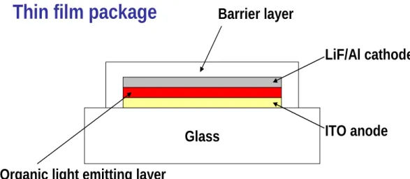
(24) same packaging method as in LED. However, minute quantity of moisture still permeated through the gluing epoxy and the sensitivity to moisture and oxygen in OLED.. As a result, a desiccative was implemented inside the display between the. glass substrate and glass lid to getter moisture. Still, glass packaging has several critical disadvantages such as cracks and impact resistance, in addition to weight and high cost concern. For example, as to cell-phone display, a glass lid, glue and a desiccative that add up cost about 1.2 dollars. It marked about three dollars of cost not including the cost of electronic device. If it still used glass packaging in OLED which were the same as LED, it was hard to compete with LED. Hence, it was necessary to develop the thin film packaging in OLED. [23]. Glass package. Getter Glass LiF/Al cathode Gluing epoxy Glass. ITO anode. Organic light emitting layer. Figure 2.6 Schematic diagram of glass package in OLED technology.. 2.2.2 Thin Film Packaging In order to reduce the weight and cost while maintaining equal or better moisture/oxygen resistance, recent thrusts in OLED packaging focused on the development of a thin-film barrier such as polymers, ceramics or their composites as 11.
(25) illustrated in Fig. 2.7. The selection of polymers included parylenes, cyclotene, etc. [24, 25] and the selection of ceramics included oxide- or nitride- base barrier films such as SiOx, AlOx, SiNx, SiOxNy, etc. [25-34] Thin film barriers have usually been formed on Al or other metal layers. Traditionally, bulk oxides and Al were effectively impermeable to oxygen and moisture, as perfect barrier films. [26, 35, 36] But traditional single thin film barrier layers did not provide the moisture/oxygen resistance we wished, whether deposited by plasma-enhanced chemical vapor deposition (PECVD), sputtering, or e-beam evaporation and Table 2.2 showed some reported water vapor resistance properties of passivation layers. [30-34] However, these reported barrier films still showed too high WVTR and OTR for OLED’s applications. This limit was attributed to defects or pinholes contained in the thin films during deposition compared to the bulk of the barrier film. [26]. Table 2.2 Some reported water vapor resistance properties of passivation layers. Material. Deposition method. Thickness. WVTR. (nm). (g/m2-day). Reference. SiOx. Reactive evaporation. 70. 0.3. [30]. SiOx. PECVD. 12. 0.15. [31]. SiNx. PECVD. 30. 0.15. [32]. AlOxNy. Sputter. 55. 0.1. [33]. AlOx. Ebeam. 30. 0.17. [34]. 12.
(26) Thin film package. Barrier layer LiF/Al cathode. Glass. ITO anode. Organic light emitting layer Figure 2.7 Schematic diagram of thin-film barrier package in OLED technology.. To overcome the deficiency of thin film inorganic barrier, Vitex System Inc. announced a novel barrier, [7, 8] BarrixTM comprised of alternating layers of polymer and ceramic film deposited in vacuum to achieve very low moisture and oxygen permeation through the filling of pinhole and defects in inorganic layers by polymer and the tortuous path in the stacking as shown in Fig. 2.8. By stacking multi-layer of organic and inorganic thin films to about 3 μm, BarrixTM layers can meet the requirements of WVTR for OLED applications. However, the deposition process as shown in Fig.2.9 seemed very complicated and needed many procedures. Hence, the cost and thermo-mechanical integrity of such ceramic/polymer multiple-layer structure (BarrixTM layer) remained a lingering issue.. 13.
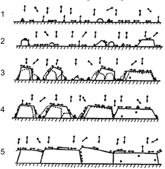
(27) Figure 2.8 Organic/inorganic multi-layer structure from Vitex Systems. (Reproduced courtesy of Vitex Systems.)[7, 8]. Figure 2.9 The deposition process of BarrixTM layers. [7, 8]. 2.3 Microstructure of Thin Films The quality of thin films in the OLED stack was closely related to its effectiveness as moisture and oxygen barriers. [26, 37] Hence, the growth process of thin film needed to be understood and reviewed below. Thin films were usually formed by deposition which was a process through continuous stages as shown in Fig.. 14.
(28) 2.10. [38, 39] First, deposited particles arrived to the substrate surface. Then nucleation was generated on the substrate surface and islands grow. Next, islands were coalesced by surface diffusion and eventually a continuous layer was formed. Either layer-by-layer (epitaxial) or island (nonepitaxial) growth of thin layers would be chose by the interfacial energy of deposited atom-deposited atom and deposited atom-substrate atom. If the interfacial energy between deposited atom and deposited atom was higher, island growth would be favored. If the interfacial energy between deposited atom and substrate surface was higher, epitaxial growth would be favored. In conclusion, the evolution of the structure in thin films was very complicated and presented different features in different stages of thin film growth.. 1 2. 3. 4. 5 Figure 2.10 Schematic diagram illustrating fundamental growth processes. The growth of thin films progresses through consecutive stages: stage1 is nucleation, stage 15.
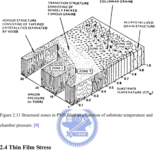
(29) 2 is island growth, stage 3 is coalescence of islands, stage 4 is formation of polycrystalline islands and channels, and stage 5 is development of continuous structure and thickness growth. [39]. The microstructure of the developing film would be characterized by the shape of its grain structure. The grain structure was affected by the growing environment such as substrate temperature, surface roughness, chamber pressure, the cleanliness levels, etc. [9, 40-42] For example, low substrate temperature led the grain growth to amorphous or polycrystalline. Thornton [9] presented a diagram which considered the effect of chamber pressure and substrate temperature on the structures of PVD films as shown in Fig. 2.11. There were four types of grain structure shapes as a function of substrate temperature and chamber pressure. In Zone I, the layer was either amorphous or fiber shape, the texture was random, and crystallite size was about 5–20 nm diameter. In Zone T, the grains had quite different sizes with increasing temperature. The structure was inhomogeneous along the film thickness. Near the substrate, the microstructure consists of randomly small grains and out of which was V-shaped columns with the favored orientations. Voids existed both in Zone I and T. In Zone II, the homogeneous grain structure was columnar shape and the diameter increases with film thickness. Zone III represented the globular structure which was developed by lateral grain growth and this structure was usually grew in the high substrate temperature range. [9, 38, 39] According to the above discussion, it was well known that the morphology of thin film and its grain structure can be controlled by the deposition parameters. On the moisture and oxygen resistance issue, the dense films with amorphous structure and low defects were desired to serve as the passivation layer in the OLED packaging.. 16.
(30) Figure 2.11 Structural zones in PVD films as a function of substrate temperature and chamber pressure. [9]. 2.4 Thin Film Stress The source of thin film stress included intrinsic stress and thermal stress which depends on their cause mechanisms. [10, 11] Intrinsic stress was caused during thin film deposition and lattice parameters mismatch of the film and substrate. Therefore, the value of intrinsic stress can be controlled by changing the deposition parameters. It may be affected by the defects in thin film, ion bombardment to the surface of films, and different atomic arrangement, etc. However, the definition of intrinsic stress was still under discussion. Thermal stress was contributed by CTE mismatch and temperature difference. When the temperature was changed of a thin film on a substrate, a strain was introduced because of the different thermal expansion coefficients and the expression 17.
(31) is. ε film = (α film − α substrate )ΔT. (2.5). where αfilm and αsubstrate are the thermal expansion coefficients of the film and substrate, respectively. Then, stress in the thin film can be determined by the expression (2.6). σ = Eε. (2.6). Finally, the calculation of the strain in (2.5) can be used in (2.6) to derive the thermal stress in thin films.. 18.
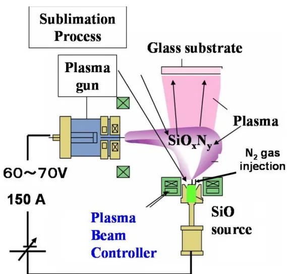
(32) Chapter 3 Experimental 3.1 Deposition System For the deposition of Al cathode or passivation film onto OLED, conventional sputtering could cause serious radiation damage to the underlying organic layer in OLEDs due to the energetic ions, electrons and x-rays produced during deposition, while plasma-enhanced chemical vapor deposition (PECVD) method can readily damage OLED device because of the toxic, reacting gases and high deposition temperature involved in the deposition process. Therefore, evaporation technique has been widely adopted in the deposition of the passivation layer for the OLEDs to avoid thermal decomposition or plasma damage. [43-45] However, in order to reduce the coast in production, the deposition rate should be high and the required number of barrier layers shall be the minimum. Therefore, an Ar ion beam evaporation system designed for continuous process was chosen for almost all layers and organic layer such as Alq3 in the preparation of OLED. [46] The schematic diagram of the Ar ion beam evaporation system for depositing moisture barrier layers and Al films devices in this study was illustrated in Fig. 3.1. The vacuum chamber was vacated until the pressure was lower than 1.0×10⁻⁴ Pa before deposition was initiated. Argon and nitrogen gases were injected into the chamber, and the pressure was about 0.1 Pa. Argon gas was injected into arc plasma generator and the argon gas became arc discharge plasma by applying appropriate power. SiO2 or Al ingots were evaporated by arc discharge plasma onto crucibles, and the SiOxNy films and Al films were then deposited on glass substrates. The deposition temperature was controlled by the distance between source and glass plate, and the horizontally moving speed of glass plate. Furthermore, the particle energy arriving to the surface of OLED structure was about 25 eV. This was lower than the energy from 19.
(33) the sputter system which was more than 100 eV as shown in Fig. 3.2. Thereby, this system would not damage the underlying Alq3 layer and could be practically used for OLED manufacturing.. Figure 3.1 The schematic diagram of an argon ion-beam evaporation system. (Courtesy of China Picture Tube, Inc.). 20.
(34) Relative Intensity. Particle energy arriving the surface of this deposition system (~25 eV). Particle energy for sputter system. Energy (eV). Figure 3.2 Energy distributions of the particle arriving to the substrate surface for conventional sputtering system and Ar ion beam evaporation system. (Courtesy of China Picture Tube, Inc.). 3.2 Sample Preparation Silicon oxynitride (SiOxNy) passivation layers and electrode Al films were deposited by using a modified Ar ion beam evaporation technique. In our deposition system, thermally energetic silicate-containing molecules were evaporated from SiO2 or Al crucible, which was heated by Ar ion beam bombarding the exterior of crucible, and deposited onto substrates.. The deposition system was also equipped with gas. lines next to SiO2 source. For example, silicon oxynitride was formed by blowing N2 during the evaporation of SiO2. The deposition temperature was controlled by the distance between source and glass plate, and the moving speed of glass plate. In this study, 600 Å thick silicon oxynitrides films were deposited onto Al (2000 Å)/Alq3 (10 Å)/glass at different substrate temperatures (60, 80 and 90 oC) with different N2 flow rates from 300 sccm to 480 sccm. Specifically, 480 sccm is designated as the high flow rate condition, while 300 sccm is designated as the low flow rate condition in 21.
(35) this study unless stated otherwise. The film thicknesses of SiOxNy barrier/Al/Alq3 /glass and the stack structure of samples used in this study were shown in Fig. 3.3. In addition, their deposition conditions were listed in Table 3.1. The effects of substrate temperature and flow rates on the microstructures (crystallinity and grain size), morphology, defects in barrier layers and its correlation with water permeation were investigated in this thesis.. SiOxNy. 600Å. Al. 2000Å 10Å. Alq3. 600μm. glass. Figure 3.3 The film thickness and stack structure of samples.. Table 3.1 Deposition parameters of SiOxNy barrier layer. SiOxNy barrier. Flow rate. Substrate temperature. Best Case. High N2. 60 ℃、80 ℃ 、90 ℃. (480sccm) Worst Case. 60 ℃、80 ℃ 、90 ℃. Low N2 (300sccm). 22.
(36) 3.3 Experimental Procedure As illustrated by the flow chart shown in Fig. 3.4, the chemical structure and composition of the oxynitride films were investigated using x-ray photoelectron spectroscopy (XPS) (VG Scientific, Microlab 350F). The frequency of Si-O-Si bond stretching vibration was obtained by specular reflectance FTIR spectroscopy (Perkir Elmer Spectrum 100). The moisture barrier effectiveness was first measured by a calcium button test (Courtesy of China Picture Tube, Inc.). Then, the relationship between moisture resistance and the microstructure of barrier layers was investigated. The morphology and microstructures of silicon oxynitride and aluminum films were examined by a scanning electronic microscopy/EDX (SEM/EDX) (JEOL JSM-6700F) and a transmission electron microscopy (TEM) (Philips TECNAI 20), respectively. In addition, grain sizes of aluminum films were obtained from an x-ray diffraction (XRD) (Siemens D5000). Defects such as Al hillock and its densities were further quantified using an Al wet etch decoration method in conjunction with optical microscope. The surface roughness of passivation layers and the maximum height of hillocks were characterized by an atomic force microscope (AFM) (Veeco D5000). Moreover, the effect of as-deposited stress on the formation of hillock defects was examined. The stress of the multi-layer was obtained from bending beam system to measure the curvature radius of the SiOxNy/Al/Alq3/glass sample. In the following section, characterization methodologies for moisture barrier, hillock defects, residual stress, and chemical structure, and analytic instrumentation such as SEM, TEM, XRD, AFM, nanoindenter, specular reflectance FTIR, XPS and bending beam would be briefly described in the following sections.. 23.
(37) Figure 3.4 Flow-chart of experimental procedures.. 24.
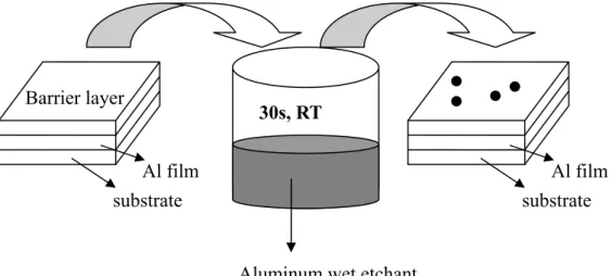
(38) 3.4 Characterization Methodologies 3.4.1 Decoration of Al Hillock Defect by a Selective Etching Process Although SEM and EDX were employed to identify the existence of Al hillock breaking through passivation layer, these techniques were not suitable to quantify the density of hillocks due to the field size, time and cost. Therefore, it was highly desirable to develop a selective, wet etching process to remove the extruded Al over the surface of passivation layer, for example, silicon oxynitride, such that hillock defects were decorated as holes, which can be detected easily using an optical microscope. The typical wet etching chemicals for SiO2, Si3N4 and Al, the chemical reactions involved, and application were summarized in Table 3.2, Table 3.3 and Table 3.4, respectively. Although phosphoric acid solution could etch silicon nitride, it still required relatively high operating temperature, at 150 to 200 ℃ . Therefore, aluminum wet etchant (composition: 80% phosphoric acid, 5% acetic acid, 5% nitric acid, and 10% water) was used to etch the SiOxNy/Al/Alq3/glass samples at 42 to 45 o. C to provide excellent selectivity (Al to SiOxNy). The typical etching time used in. this study was 30 seconds and the wet etching process was schematically shown in Fig. 3.5.. 25.
(39) Barrier layer. 30s, RT. Al film substrate. Al film substrate. Aluminum wet etchant (Phosphoric acid, acetic acid, nitric acid and water). Figure 3.5 Schematic diagrams of etching process for decoration of Al hillocks.. Table 3.2 Description of wet etching SiO2 layer. [47] Etching material. SiO2. Etchant. •. Hydrofluoric Acid (HF) Solution. •. Normally diluted in buffer solution or DI water to reduce etch rate.. Reaction Applications. SiO2. + 6HF Î. H2SiF6 + 2H2O. •. Widely used for CVD film quality control. •. BOE: Buffered oxide etch. 26.
(40) Table 3.3 Description of wet etching Si3N4 layer. [47] Etching material. Si3N4. Etchant. •. Reaction Applications. Hot (150 to 200 °C) phosphoric acid H3PO4 Solution Si3N4. +. 4 H3PO4. Î Si3(PO4)4 + 4NH3. •. High selectivity to silicon oxide. •. Used for LOCOS and STI nitride strip. Table 3.4 Description of wet etching Al layer. [47] Etching material. Al. Etchant. •. Heated (42 to 45 °C) solution. •. One example: 80% phosphoric acid, 5% acetic acid, 5% nitric acid, and 10 % water. Reaction. •. Nitric acid oxidizes aluminum and phosphoric acid removes aluminum oxide at the same time.. Applications. •. Acetic acid slows down the oxidation of the nitric acid.. •. High selectivity to silicon oxide. •. Used for ULSI process. 3.4.2 Ca Button Test for Moisture Permeation The moisture resistance of barrier layers was qualitatively examined by a Ca button test through the observation of the corrosion of calcium. Typically, the barrier layers such as SiOxNy films were deposited onto a 300Å thick calcium on a glass plate. This test was carried out in an oven at 60 oC and 90% relative humidity for 15 minutes or at room temperature and humility for 66 hours. Then, the reacted sites could be observed as spots on the Ca film and the permeability of different materials could be. 27.
(41) compared. The detail of this method is mentioned in Chapter 2.1.3.. 3.5 Instrumentation and Data Analysis 3.5.1 FE-SEM Field-emission scanning electron spectroscopy (FE-SEM) (JEOL 6700F) was employed to investigate the morphologies of barrier layers. FESEM is a powerful analysis tool to characterize microstructure down to several ten nanometers.. 3.5.2 HR-TEM High resolution transmission electron microcopy (HRTEM) (Philips Tecnai 20) was used to obtain high magnification and high resolution image of cross-sectional image of SiOxNy/Al bi-layer. Information obtained from TEM is not only the high resolution image but also the crystal structure, orientations and chemical compositions.. 3.5.3 X-ray Diffraction (XRD) XRD (Siemens D5000) was employed to characterize the crystallite sizes of aluminum films. The operation voltage of the XRD used in this measurement was 40 kV and the operation current was 30 mA. The X-ray was used the characteristic peak Kα of Cu (λ=1.5406Å) which was filtered by Ni-filter. The detector scanned the samples between 2θ= 10-90 degrees. The crystallite sizes of aluminum films can be calculated by the full width at half maximum of the dominant Al (111) peak in XRD patterns schematically illustrated by Fig. 3.6, according to Scherrer’s equation (3.1) [48]. t=0.9λ /Bcosθ. (3.1). where t is the crystallite size, λ is the wavelength for Cu Kα, B is the full width at half 28.
(42) maximum and θ is the diffraction angle.. Figure 3.6 XRD patterns of crystalline film with finite crystallite size. [48]. 3.5.4 Atomic Force Microscope (AFM) AFM (Veeco D5000) was employed to quantify the surface roughness of passivation layers and the maximum height of hillocks in a tapping mode. In operation, the cantilever was biased with AC and DC voltage and sensed the distance between the tip and the sample surface by Van der Waal’s force. As the interaction force changed between the cantilever tip and the surface, the deflections of the cantilever were varied. Then, the deflections were measured and derived a topographic image of the surface.. 3.5.5 Nanoindentation Young’s modulus of glass substrate was measured by nanoindentation. A MTS Nano Indenter XP system in Nano-Device Lab with a three-side pyramid (Berkovich) tip was employed in a continuous stiffness mode (CSM) and at a constant strain rate 0.05 s- 1. The load–displacement relation was used to evaluate the mechanical properties of samples as shown by Fig. 3.7. For a single film structure, Oliver and Pharr analysis method was employed for nanoindentation measurement to derive Ef. 29.
(43) [49]The reduced Young’s modulus, Er can be obtained by Equation 3.2:. π S π 1 dP Er = = 2 β A 2 β A dh. (3.2). where Er: reduced modulus ß: constant depending on the geometry of the indenter A: projected area of elastic contact S=. dP : the slope of the load–displacement curve at the beginning of the unloading dh. stage as illustrated in Fig. 3.8.. Then, Er can be further expressed in terms of film and indenter by Equation (3.3):. (1 − ν 1 = Er Ef. 2 f. ). (1 − ν i2 ) + Ei. (3.3). where Ei, vi: Modulus and Poisson's ratio of the indenter Ef, vf: Modulus and Poisson's ratio of the specimen Finally, the modulus of thin film (Ef) was rearranged as a function of penetration depth in our measurement and derived by combining Equation (3.3) and (3.4).. Ef =. (1 − ν 2f ) 1 (1 − ν i2 ) − Er Ei. 30. (3.4).
(44) Figure 3.7 Load-Displacement of Nanoindentation. [49]. 3.5.6 Specular Reflectance Fourier-Transform Infrared Spectroscopy (Specular Reflectance FT-IR) Since Al film is a good reflective mirror in SiOxNy/Al/glass sample stack, specular reflectance FTIR spectroscopy (Perkir Elmer Spectrum 100) was employed to examine the chemical make and structural information of SiOxNy. In particular, Si-O-Si bond stretching frequency in SiOxNy thin film samples was measured by a specular reflectance apparatus VeeMAX [50] at 40o incident angle as schematically shown in Fig. 3.8. The specular reflectance infrared spectra were collected in 500-4000 cm-1 range with a resolution of 4 cm-1.. 31.
(45) Glass Al SiOxNy. Incident IR light Figure 3.8 Schematic diagram of a specular reflectance infrared spectroscopy.. 3.5.7 X-ray Photoelectron Spectroscopy (XPS) The composition and chemical bonding of the oxynitride films were investigated using XPS (VG Scientific, Microlab 350F). The photoelectron emission spectra were obtained using an Mg Kα X-ray source (E=1253.6 eV) striking the surface of the sample. The analyzer resolution was fixed at 0.01 eV. Ar+ ion was used to remove adsorbed surface contaminants for 5 seconds before analysis. The insulating properties of these deposits caused surface charging effects, resulting in electron lines being shifted to lower kinetic energies. [51] The peak positions were calibrated with respect to the position of C 1s carbon contamination peak usually located at about 285 eV.. 32.
(46) 3.5.8 Bending beam system 3.5.8.1 Evolution of Stoney’s Equation If the film deposited on the substrate is under stress, it will result in a bending to maintain mechanical equilibrium. And if the film is very thinner than the substrate and the stress in the film is linear related to the curvature of the substrate that the relationship was deduced by G. G. Stoney in as early as1909. [52] Stoney’s equation is. σ =. E s t s2 1 6(1 − ν s )t f R. (3.5). Since the substrate is not absolutely flat in many cases, it may have its initial curvature. Thus, Equation (3.5) should be deduced by subtracting the initial curvature ( 1 / R0 ) from the measured curvature ( 1 / R ). Stoney's equation becomes:. σ =. E s t s2 6(1 − ν s )t f. ⎛1 1 ⎞ ⎟⎟ ⎜⎜ − ⎝ R R0 ⎠. (3.6). where Es and υs are the Young’s modulus and Poisson’s ratio of the substrate, and tf and ts are the thicknesses of the film and substrate. R0 is the radius of curvature of the uncovered substrate and R is the radius of curvature with the film on the substrate. Therefore, the stress can be determined by measuring the curvature of the sample in conjunction with the only parameter, thickness of thin film and Young’s modulus and Poisson’s ratio of the substrate, which can be obtained from literatures. Consequently, Stoney's equation has been extensively used for thin film stress studies through curvature measurement.. 33.
(47) 3.5.8.2 Bending Beam System The schematic diagram of the bending beam system was illustrated in Fig.3.9. The sample (thin film/substrate) in free standing form was put inside the copper heater block, which can be heated up to 450 oC, in the vacuum chamber. Two parallel laser beams were directed onto the sample at two different positions and then were reflected to two position-sensitive detectors as shown in Fig.3.10, in which D is the spacing of two incident laser beam. L is the distance between the sample and position-sensitive detector. S is the spacing of two reflected laser spots on detector. S0 is the spacing of the bare substrate from two reflected laser spots on detector. 1/R is the curvature of the substrate with film, and 1/R0 is the curvature of the bare substrate. Then, the change of the curvature could be derived by the following expression (Stoney's equation):. E s t s2 σ = 6(1 − ν s )t f. ⎛1 1 ⎞ ⎟⎟ ⎜⎜ − R R 0 ⎠ ⎝. (3.6). From the geometry relationship in Fig.3.10, tan θ ≈. D/2 D = ≈ θ , since θ → 0 R 2R. tan 2θ ≈. D a = R L. (3.7) (3.8). Hence, 1 a = R DL. (3.9). With the same principle, b 1 = R0 DL. (3.10). Equation (3.3) in substitution for (3.6) and (3.7) becomes:. 34.
(48) E s t s2 ⎛ a − b ⎞ σ= ⎜ ⎟ 6(1 − ν s )t f ⎝ DL ⎠. (3.11). In addition, ΔS = S 0 − S = 2(a − b). (3.12). Equation (3.11) in substitution for (3.12) becomes:. E s t s2 ⎛ ΔS ⎞ σ= ⎜ ⎟ 6(1 −ν s )t f ⎝ 2 DL ⎠. (3.13). Finally, thin film stress using bending beam system and Stoney’s equation was derived. In order to increase the sensitivity and accuracy of the measurement, film thickness/substrate thickness needed to be less than 1/1000 and the sample size was close to 5 cm long and 1 cm wide. In our experiment, the sample was cut to 5 cm long and 1 cm wide. The total film thickness/substrate thickness is about 0.25 μm/600 μm which is less than 1/1000. In order to reduce the noise caused by sample vibration at temperature higher than 300 oC, the chamber was first evacuated to 6 mTorr, then introduced with N2 to 50 Torr. Typically, the heating rate was 2℃/min in the heating cycle, then nature cooling as employed in the cooling cycle. Since the S0 cannot be obtained by etching the film off the transparent glass substrate, the selected S0 can be estimated by (positive S+ backside S)/2 in this study.. 35.
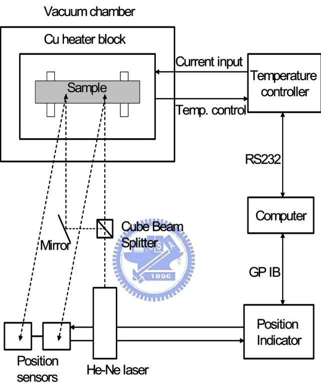
(49) Vacuum chamber Cu heater block Current input. Temperature controller. Sample Temp. control. RS232. Mirror. Cube Beam Splitter. Computer. GP IB. Position Indicator Position sensors. He-Ne laser. Figure 3.9 Schematic setup of a bending beam system for stress measurement.. 36.
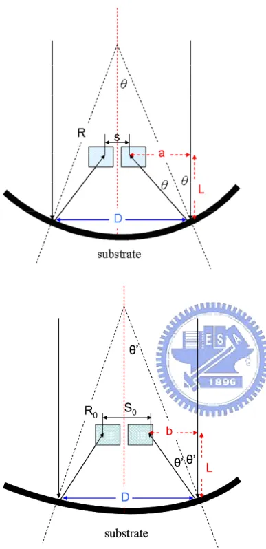
(50) s. θ’. R0. S0. b θ’ θ’ L D substrate. Figure 3.10 Schematic diagram of the laser routes in the bending beam system. D is the spacing of two incident laser beam. L is the distance between the sample and position-sensitive detector. S is the spacing of two reflected laser spots on detector. S0 is the spacing of the bare substrate from two reflected laser spots on detector. 1/R is curvature of the substrate with film. 1/R0 is curvature of the bare substrate.. 37.
(51) 3.6 Grain Size Analysis of Al by IMAGE J The distribution of grain size in SEM viewgraph was analyzed and compiled using Image J software, which is a public domain Java image processing program available from US National Institutes of Health (NIH). [57]The procedure of grain size analysis by Image J can be detailed as follow. First, we demarcated the grain area of SEM top-view graph as shown in Fig. 3.11. Then, the contrast of image was adjusted to black and white using Image J as shown in Fig. 3.12. After enhancing the contrast, the distribution of grain size was analyzed by using AnalyzeÎ Analyze particles command as shown in Fig. 3.13 with result shown in Fig.3.14.. Figure 3.11 SEM image which has been demarcated the grain area.. 38.
(52) Figure 3.12 Illustration of altering interactively the brightness and contrast of the image to be relative block and white.. 39.
(53) Figure 3.13 Location of the command “Analyze Particles”.. 40.
(54) Figure 3.14 Analysis result of grain size distribution.. 41.
(55) Chapter 4 Results and Discussion 4.1 Chemical Structure and Composition Analysis of SiOxNy Layers 4.1.1 Analysis by Specular Reflectance FTIR Spectroscopy The Si-O structural information of SiOxNy films was first obtained from the Si-O-Si stretching vibration using specular reflectance FTIR spectroscopy. Fig. 4.1 showed Si-O-Si infrared absorption peaks of three types of passivation layer deposited at fixed substrate temperature (80 ℃): (1) pure SiO2 (2) SiOxNy under low nitrogen flow rate, and (3) SiOxNy under high nitrogen flow rate, whose FTIR absorption peak positions were summarized in Table 4.1. The Si-O-Si absorption peak was 1208 cm-1 for pure SiO2 layer, 1176 cm-1 for passivation films deposited under high flow rate condition, and 1171 cm-1 for passivation films deposited under low flow rate condition. The Si-O stretching band of SiOxNy films shifted to lower wavenumber with decreasing N2 flow rate. This indicated that a change of chemical environment by the increased incorporation of Si-N bonding, whose stretching frequency was typically at 980 cm-1, contributed the down-shifting of Si-O stretching bands. Moreover, it implied that the lower nitrogen flow rate generated higher nitrogen content of the oxynitride based on the Si-O infrared peak position. [56]. Table 4.1 Si-O absorption peak position of three types of passivation layer. Passivation layer. Absorption Peak Position (cm-1). SiO2. 1208. SiOxNy under high flow rate. 1176. SiOxNy under low flow rate. 1171. 42.
(56) 0.020. SiOxNy_high flow rate SiOxNy_low flow rate SiO2. Absorbance. 0.015. 0.010. 0.005. 0.000. -0.005 1400. 1200. 1000. 800. 600. -1. wavenumber(cm ) Figure 4.1 Specular reflectance FTIR spectrum of three types of passivation layer: (1) pure SiO2, (2) SiOxNy under high nitrogen flow rate, and (3) SiOxNy under low nitrogen flow rate.. 4.1.2 Composition Analysis by XPS The XPS Si 2p, N 1s, and O 1s spectra of oxynitride films deposited under 80 ℃ and different flow rate conditions were shown in Figs. 4.2 (a) and (b).. The. integrated areas of these peaks, summarized in Table 4.2 and 4.3, were used to quantify the surface composition. It showed the surface composition of oxynitride films deposited under 80 ℃ and low flow rate condition was SiO0.7N1.9. In contrast, the surface composition of oxynitride films deposited under 80 ℃ and high flow rate condition was SiO0.67N2.0. Nitrogen content in films deposited under high flow rate was found to be slightly less than under low flow rate condition, which was consistent with the finding from infrared spectroscopy. It can be inferred that less N atoms could. 43.
(57) be dissociated because the plasma energy was dispersive under high N2 flow rate condition. Also, high flow rate yielded high chamber pressure and shorter mean free path. Hence, less N atoms could be incorporated into the passivation film. Overall, the difference in composition under various flow rate conditions was not significant.. 50000. 40000. Si 2p. Si 2p. 35000. 40000. Counts/s. Counts/s. 30000 30000. 20000. 25000 20000 15000 10000. 10000. 5000 0 110. 108. 106. 104. 102. 100. 98. 0 110. 96. 108. 106. 104. 102. 100. 98. 96. Binding energy (eV). Binding energy (eV) 55000. N 1s. 60000. N 1s. 50000 45000. Counts/s. Counts/s. 50000. 40000. 30000. 40000 35000 30000 25000. 20000. 20000 15000. 10000. 404. 402. 400. 398. 396. 394. 392. 404. 390. 180000. 398. 396. 394. 392. 390. O 1s. 140000. 140000. 120000. Counts/s. 120000. Counts/s. 400. 160000. O 1s. 160000. 100000 80000. 100000 80000 60000. 60000. 40000. 40000. 20000. 20000 540. 402. Binding energy (eV). Binding energy (eV). 538. 536. 534. 532. 530. 528. 540. 526. 538. 536. 534. 532. 530. 528. 526. Binding energy (eV). Binding energy (eV). (a). (b). Figure 4.2 The XPS Si 2p, N 1s, and O1s spectra of oxynitride films deposited under 80 ℃ (a) low flow rate and (b) high flow rate conditions. The references of Si 2p signals: Si-Si (99.4 eV), Si-N (101.9 eV), and Si-O (103.4 eV). [58]. 44.
(58) Table 4.2 Binding energies and composition quantification of oxynitride film deposited under 80 ℃ and low flow rate condition. Name. Peak BE. Area. Atomic fraction (%) Si : N : O. Si 2p. 102.31. 166.07. 27.6. 1. N 1s. 397.86. 114.3. 19.1. 0.7. O 1s. 532.65. 319.88. 53.3. 1.9. Table 4.3 Binding energies and composition quantification of oxynitride film deposited under 80 ℃ and high flow rate condition. Name. Peak BE. Area. Atomic fraction (%) Si : N : O. Si 2p. 102.27. 140.84. 27.1. 1. N 1s. 397.80. 94.98. 18.2. 0.67. O 1s. 532.65. 284.96. 54.7. 2.0. 4.2 Morphology and Microstructure of Barrier Layers/Al Samples The morphology and microstructures of silicon oxynitride/aluminum/Alq3/glass samples were examined first by SEM. Figs.4.3 (a) and (b) showed the morphology of SiOxNy passivation films deposited at substrate temperature of 90℃, under high and low flow rates, respectively. Both showed not only no significant difference in the grain sizes between high and low N2 flow rate conditions, but also no pinhole formation. However, unknown bump was observed widespread over the surface of samples by top-view SEM as shown in Fig. 4.4 (a). These widespread defects. 45.
(59) represented by SEM in Fig. 4.5(a) were identified to be Al hillocks by electron diffraction spectrometry (EDS), whose composition was listed in Table 4.4. This indicated that large topographic changes occurred in the underlying Al film, and some of the Al hillocks broke through SiOxNy passivation film. These Al extrusions would cause damage in passivation layer and lead to moisture permeation. In addition, Fig. 4.4 (b) showed crack defect, which was very minor and negligible as the root-cause of moisture permeation. Thus, based on the quantity, hillock defects were the most probable root-cause for moisture permeation. In order to statistically quantify the hillock density of various SiOxNy films and find any correlation with moisture permeation, an Al wet etch method was employed to decorate hillock defects using aluminum wet etchant (composition: 80% phosphoric acid, 5% acetic acid, 5% nitric acid, and 10% water). Extruded Al was removed readily by Al wet etchant leaving holes as validated by SEM illustrated in Fig. 4.5 (b). Therefore, optical microscope could readily used to quantify Al hillock density together with Image J as described in Chapter 4.3.. Figure 4.3 SEM top-view graphs of the SiOxNy films deposited at substrate temperatures 90℃: (a) under high flow rate, (b) under low flow rate.. 46.
(60) (a). (b). Figure 4.4 SEM top-viewgraphs tilted 52º of the SiOxNy films: (a) unknown bump, (b) crack.. Figure 4.5 SEM photographs: (a) defects of Al hillock and (b) topography after wet etch of Al hillocks. Table 4.4 EDS analysis of the defect shown in Fig. 4.5 (a). Element. Atomic %. OK. 56.03. Al K. 26.09. Si K. 14.34. Cl K. 3.55. Total. 100.00 47.
(61) 4.3 Hillock Formation 4.3.1 Hillock Density Hillock densities of the SiOxNy/Al films deposited under different flow rates and various substrate temperatures were further quantified using an Al wet etch method for defect decoration and optical microscope for inspection as shown in Figs.4.6 (a)-(f) and summarized in Table 4.5. SiOxNy/Al samples possessed lower Al hillock density as substrate temperature increased or flow rate increased. The correlation between hillock density and moisture permeation through SiOxNy/Al samples was further discussed in Chapter 4.4.. Table 4.5 Al hillock density of the SiOxNy/Al films deposited under different flow rate condition at various substrate temperatures. Hillock density (10-5/µm2) Substrate Temperature (℃). 60. 80. 90. High. 41.4. 34.6. 7.9. Low. 74.8. 40.8. 14.7. N2 flow rate. 48.
(62) (a). (d). (b). (e). (c). (f). Figure 4.6 OM photographs magnified 1000x: under low flow rate at various substrate temperatures: (a) 60 ℃, (b) 80℃, and (c) 90℃ and under high flow rate at various substrate temperatures: (d) 60 ℃, (e) 80℃, and (f) 90℃.. 49.
(63) 4.3.2 Hillock Height The maximum height of hillocks of silicon oxynitrides deposited under various deposition conditions (flow rates and deposition temperatures) were characterized by AFM as shown in Figs. 4.7 (a)-(f) and summarized in Table 4.6. As substrate temperature increased, the hillock height increased. In contrast, the maximum hillock heights in the films deposited under high flow rate conditions were slightly higher than those deposited under low flow rate conditions.. Table 4.6 The maximum height of hillock of the SiOxNy/Al films deposited under different flow rate condition at various substrate temperatures. Max. height (nm) Substrate Temperature (℃). 60. 80. 90. High. 34.8. 54.2. 70.6. Low. 24.8. 38.1. 68.6. N2 flow rate. (a). 50.
(64) (b). (c). (d). 51.
(65) (e). (f) Figure 4.7 AFM 2D images (2μm×2μm): (a) substrate temperature is 90℃ under high flow rate, (b) substrate temperature is 90℃ under low flow rate, (c) substrate temperature is 80℃ under high flow rate, (d) substrate temperature is 80℃ under low flow rate, (e) substrate temperature is 60℃ under high flow rate, and (f) substrate temperature is 60℃ under low flow rate.. 52.
數據
+7
![Figure 3.6 XRD patterns of crystalline film with finite crystallite size. [48]](https://thumb-ap.123doks.com/thumbv2/9libinfo/8630253.192297/42.892.136.475.143.413/figure-xrd-patterns-crystalline-film-finite-crystallite-size.webp)
相關文件
在1980年代,非晶矽是唯一商業化的薄膜型太 陽能電池材料。非晶矽的優點在於對於可見光
• Many statistical procedures are based on sta- tistical models which specify under which conditions the data are generated.... – Consider a new model of automobile which is
In part II (“Invariance of quan- tum rings under ordinary flops II”, Algebraic Geometry, 2016), we develop a quantum Leray–Hirsch theorem and use it to show that the big
The results contain the conditions of a perfect conversion, the best strategy for converting 2D into prisms or pyramids under the best or worth circumstance, and a strategy
For pedagogical purposes, let us start consideration from a simple one-dimensional (1D) system, where electrons are confined to a chain parallel to the x axis. As it is well known
Without using ruler, tearing/cutting of paper or drawing any line, use the square paper provided (Appendix A) to fold the figure with the same conditions as figure 8b, but the area
Experiment a little with the Hello program. It will say that it has no clue what you mean by ouch. The exact wording of the error message is dependent on the compiler, but it might
Therefore, this study will be conducted under different humidity conditions, aluminum honeycomb plate under four point bending static and fatigue strength of the experiments
