國 立 交 通 大 學
電子物理研究所
博 士 論 文
自聚性二六族半導體量子點之成熟機制
與特性研究
Ripening Dynamics and Characterization on
Self-Assembled II-VI Semiconductor Quantum Dots
研究生:賴怡仁
指導教授:周武清 博士
自聚性二六族半導體量子點之成熟機制與特性研究
Ripening Dynamics and Characterization on Self-Assembled
II-VI Semiconductor Quantum Dots
研 究 生:賴怡仁 Student:Yi-Jen Lai
指導教授:周武清 Advisor:Wu-Ching Chou
國立交通大學
電子物理研究所
博士論文
A DissertationSubmitted to Institute of Electrophysics College of Science
National Chiao Tung University in Partial Fulfillment of the Requirements
for the Degree of Doctor of Philosophy
in Electrophysics
November 2008
Hsinchu, Taiwan, Republic of China
自聚性二六族半導體量子點之成熟機制
自聚性二六族半導體量子點之成熟機制
自聚性二六族半導體量子點之成熟機制
自聚性二六族半導體量子點之成熟機制
與特性研究
與特性研究
與特性研究
與特性研究
博士生 博士生博士生 博士生::::賴怡仁賴怡仁賴怡仁賴怡仁 指導教授指導教授:指導教授指導教授:::周武清周武清周武清 周武清 博士博士博士博士 國立交通大學 國立交通大學 國立交通大學 國立交通大學 電子物理研究所電子物理研究所電子物理研究所 電子物理研究所 論 論 論 論 文 文文 文 摘摘 摘摘 要要要 要 本論文旨於探討自聚性二六族半導體量子點之成熟機制與特性分析。利用分 子束磊晶法在砷化鎵基板上成長自聚性硒化鎘/硒化鋅與碲化鋅/硒化鋅兩種量子 點結構,藉此研究各種效應(包括部份覆蓋層、活性氧原子以及快速熱退火處理) 對於成熟機制的影響。我們發現對於硒化鎘/硒化鋅異質結構而言,260 o C是成長 量子點最理想的基板溫度。藉由原子力顯微鏡的觀察,證實硒化鎘量子點結構的 形成是從二維轉變為三維的成長模式,此轉變的臨界厚度(沾溼層;wetting layer) 約2.5個原子層。隨著硒化鎘沈積量增加,我們觀察到量子點的成長模式發生一 連串的轉變,從起先的二維磊晶模式(Frank van der Merve mode)轉變為穩定的 三維成長模式(Stranski–Krastanow growth mode),最後進入成熟模式(ripened mode)。利用一個圖示的模型,我們描述了整個量子點成長模式的轉變。 針對成熟機制,我們進一步做了一系列的研究:利用硒化鎘/硒化鋅量子點 探討硒化鋅部份覆蓋層以及活性氧原子對於成熟機制的影響。從表面形貌的觀 察,發現部份覆蓋層會加快成熟機制的速度,這是由於部份覆蓋層增加了應變能 量所造成的結果;當硒化鋅部份覆蓋層厚度低於3個原子層,隨著部份覆蓋層厚 度增加,其光激螢光的能量呈現明顯的紅位移,這個結果與原子力顯微鏡觀察到 的結果是一致的。另一方面,在硒化鋅緩衝層表面鋪上活性氧原子也可以加快成 熟機制的速度,活性氧原子在硒化鋅緩衝層表面可能會改變其局部的化學性質,
並且在表面上扮演凝核中心的角色,因此,在硒化鎘沈積厚度相同的條件下,成 長在有加活性氧原子處理的硒化鋅緩衝層表面上的量子點密度會較高,且尺寸較 小。此外,我們也利用碲化鋅/硒化鋅第二型能帶結構的量子點探討快速熱退火 對於成熟機制與能帶彎曲效應的影響。自聚性碲化鋅/硒化鋅量子點也是以從二 維轉變為三維的成長模式形成量子點結構。當量子點經過400 o C以上的熱退火處 理,其光激螢光的能量會發生很大的紅位移,這是由於當熱退火溫度超過400 oC,熱能啟動了成熟機制,使得某些量子點因為聚集了鄰近小量子點的材料而尺 寸變大。在時間解析的光激螢光實驗中,較快的再結合通道被抑制了,暗示快速 熱退火處理減小了碲化鋅/硒化鋅量子點的能帶彎曲效應。最後,我們利用改變 激發光強度的光激螢光實驗證實了碲化鋅/硒化鋅量子點的能帶彎曲效應被減小 是由於熱退火啟動成熟機制造成量子點尺寸變大的關係。
Ripening dynamics and characterization on
self-assembled II-VI semiconductor quantum dots
Student: Yi-Jen Lai Advisor: Dr. Wu-Ching Chou
Department of Electrophysics, National Chiao Tung University, Hsin-Chu, Taiwan, Republic of China
Abstract
This dissertation is devoted to study the ripening dynamics of the self-assembled II-VI semiconductor quantum dots (QDs). The self-assembled CdSe/ZnSe and ZnTe/ZnSe QDs, which were grown on GaAs (001) substrate by molecular beam epitaxy (MBE), were employed to study various effects on the ripening dynamics. In the CdSe/ZnSe QDs system, the optimum growth temperature was found to be 260 oC. The Stranski–Krastanow (SK) growth mode was confirmed clearly by atomic force microscopy (AFM) images. The thickness of the wetting layer of the CdSe QDs is about 2.5 mono-layers (MLs). As the coverage increases, a complete transfer of the QD growth mode from the Frank van der Merve (FM) mode to the SK mode, followed by the ripened mode, was observed. A schematic diagram of the growth mechanism of self-assembled CdSe QDs was presented.
The effects of ZnSe partial capping and atomic oxygen on the ripening dynamics were investigated in the CdSe QDs system. AFM images show that the ripening of QDs is dramatically accelerated by the deposit of a ZnSe partial capping layer. The driving force of ripening enhancement is attributed to the increasing strain energy
with capping thickness. For a ZnSe partial capping layer of below 3 MLs, photoluminescence (PL) exhibits a clear red-shift with increasing ZnSe MLs. It is attributed to the increasing size of the CdSe QDs with the ZnSe partial capping, in a manner that is consistent with the results of the AFM study. On the other hand, the ripening of CdSe QDs can be significantly enhanced by introducing atomic oxygen and was confirmed by a PL study. The atomic oxygens on the surface of ZnSe buffer layer probably change the local chemistry of the ZnSe surface and play the role of the nucleation sites. Therefore, the incorporations of atomic oxygen cause the increasing density of QDs and the decreasing size of CdSe QDs when the CdSe coverage thickness is kept the same.
Moreover, we investigated the effect of rapid thermal annealing (RTA) on ripening and band-bending effect for the type-II ZnTe/ZnSe QDs with 3.0 MLs. The self-assembled ZnTe/ZnSe type-II QDs were grown with the SK mode. The PL spectra of samples that were annealed at temperatures of over 400 oC reveal a strong red-shift in the peak energy. This significant red-shift is understood by the QD ripening, the increasing of the dot size is caused by the migration of atoms from the neighboring smaller QDs, activated by RTA process. In a time-resolved PL study, the fast recombination channel in annealed QDs is suppressed, implying that RTA reduces band-bending effect of ZnTe/ZnSe QDs. Finally, studies of the dependences of excitation power demonstrate that the observed reduction in the band-bending effect is attributed to the increase in the dot size upon the RTA process.
致
致
致
致
謝
謝
謝
謝
俗話說:不聰明的人,就要靠努力;不努力的人,只能靠運氣。我的運氣真 的很好,回顧博士生涯的這五年,每當遇到困難與挫折的時候,總會有貴人適時 出現鼓勵我、幫助我,現在能夠感受到這份收成的喜悅,這一切都要感謝許多人 對我的提攜與幫助。 這一篇論文能夠順利完成,首先要感謝我的指導教授-周武清博士,老師悉 心的教導使我對半導體量子點有更深層的認知,在meeting上不時的討論並指點 我正確的方向,使我在這些年中獲益匪淺。老師對學問的嚴謹更是我應該學習的 典範,從老師身上我學到了不只是做研究需要要求嚴謹,做每一件事都該用嚴謹 的態度去面對。 其次,我要感謝楊祝壽學長,在我人生最低潮的時候,還好有您拉我一把, 在我孤立無援的時候,是您替我找到容身之處。雖然我總是很不受教,一再讓您 失望,但是一直到最後您都沒有放棄我,我真的好感動。因為有你的體諒及幫忙, 我才有辦法走到這一步,謝謝您。另外,我也要感謝王智祥老師,願意讓我去中 原做實驗,又放心把學弟讓我帶,不時和我討論新的想法,總讓我在遇到瓶頸的 時候能夠迎刃而解。 接著我要感謝和我一起並肩作戰過的學弟威祥、睦駕、偉傑,我的論文裡面 有你們的指紋,有你們的足跡,每一個實驗結果都是我們共同努力的結晶。你們 總是不厭其煩的聽著我用荒謬的想法解釋詭異的實驗結果,看到你們專注的眼 神,即使自己講的心虛,也會感覺有信心了,和你們一起做實驗一起討論數據的 感覺真的很開心。另外還有中原的其他學弟妹德盺、bibo、宣宣、柏盛、柏亦、 志典、黑人、胖胖、秉倫、伶臻,因為有你們貼心的服務,讓我在中原可以認真 當個足不出戶的宅男。當然,也不會忘記交大的繼祖學長、京玉學長、瑞雯學姐、
狗哥、彥丞、瑞泰、崑峰,無論是學術上的討論、還是言不及義的瞎扯,因為有 你們的陪伴讓我的研究生活變得絢麗多彩。 女友鈺旋在背後的默默支持更是我前進的動力,沒有鈺旋的體諒、包容,相 信這五年的生活將是很不一樣的光景。 最後,謹以此文獻給我摯愛的父母以及外公外婆,謝謝你們讓我能夠無後顧 之憂的完成這段求學歷程。
Contents
Abstract in Chinese I Abstract in English III Acknowledgments V Contents VII List of Tables IX List of Figures X
Chapter 1. Introduction 1
1.1 Ripening Dynamics of Quantum Dot 1
1.2 CdSe/ZnSe Quantum Dot 4
1.3 ZnTe/ZnSe Quantum Dot 5
1.4 Outline of this Dissertation 7
Chapter 2. Experimental Techniques 16
2.1 Molecular Beam Epitaxy (MBE) 16
2.2 Atomic Force Microscopy (AFM) 18
2.3 Photoluminescence (PL) 19
2.4 Time-resolved Photoluminescence (TR-PL) 20
2.5 Rapid Thermal Annealing (RTA) 21
Chapter 3. Growth Dynamics of CdSe Self-Assembled Quantum Dots 27
3.1 Growth of CdSe/ZnSe Quantum Dots 27
3.2 Optimum Growth Temperatures 30
3.4 Summary 35
Chapter 4. Effect of ZnSe Partial Capping on the Ripening of CdSe QDs 46
4.1 Sample Growth 46
4.2 Enhancement of Ripening by Partial Capping 47
4.3 Effect of the Partial Capping Thickness 50
4.4 Summary 51
Chapter 5. Effect of Atomic Oxygen on the Ripening of CdSe QDs 58
5.1 Sample Growth 58
5.2 Role of the Atomic Oxygen in CdSe QD Formation 60
5.3 Enhancement of Ripening by Atomic Oxygen 62
5.4 Summary 63
Chapter 6. Effect of Rapid Thermal Annealing on the Ripening and Band-Bending of Type-II ZnTe/ZnSe QDs 70
6.1 Sample Growth 70
6.2 Characteristic of As-Grown ZnTe/ZnSe QDs 72
6.3 Activation of the Ripening 73
6.4 Reduction of the Band-Bending effect 74
6.5 Summary 78
Chapter 7. Conclusions 86
List of Tables
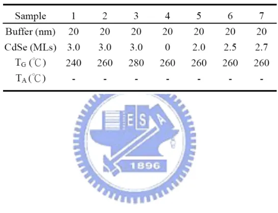
Tab. 3.1: Growth parameters of samples for studying the growth
dynamics of CdSe self-assembled quantum dots………37 Tab. 4.1: Size and density of the uncapped and partially capped CdSe
QDs obtained from AFM images……….…53 Tab. 5.1: Growth parameters of samples for studying the effect of atomic
List of Figures
Fig. 1.1: Schematic illustration of the free energy of an island as a function of island volume V. The dotted line indicates the total
free energy of strain-free island nucleation………..14
Fig. 1.2: Schematic type-II band alignment for ZnTe QDs...15
Fig. 2.1: Veeco Applied EPI 620 MBE system………...….23
Fig. 2.2: Riber 32P MBE system……….24
Fig. 2.3: NT-MDT SOLVER P47 AFM system……...…..25
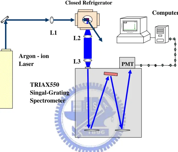
Fig. 2.4: Experimental setup for the PL measurement……….26
Fig. 3.1: AFM plane view and three-dimensional view for 3.0 MLs CdSe QD samples 1 (TG = 240 oC), 2 (TG = 260 oC) and 3 (TG= 280 o C)………..………...………38
Fig. 3.2: AFM plane view for CdSe QDs with the coverage from 0 to 3.0 MLs………..…39
Fig. 3.3: Dot size distributions of sample 2 (3.0 MLs). The dot volume was calculated by assuming the dots are conical. The two group size distributions were observed……….40 Fig. 3.4: Equilibrium phase diagram of the self-assembled QDs,
obtained by minimizing the sum of the energy of the strained overlayer, the free energy of the QDs and the total energy density of the ripened islands. The x-axis is the misfit between
the buffer layer and the material grown above. The y-axis
represents the average coverage of QD...41 Fig. 3.5: Schematic diagram of the growth dynamics for the self-
assembled CdSe QDs: (a) to (c) SK growth mode, (d) R2 growth mode, showing coexisting larger ripened QDs and
smaller coherent QDs…...………...…..42 Fig. 3.6: (a) PL spectra from capped CdSe QDs for various coverages.
The CdSe coverage increases from 1.0 to 3.3 MLs. (b) PL peak position depends on the CdSe coverage, and two slopes are
observed………...………...…..43 Fig. 3.7: Activation energy (Ea) versus CdSe coverage.………..…44 Fig. 3.8: Lines A and B represent the PL intensity of CdSe QDs with
coverages of 2 MLs and 2.8 MLs, respectively. Line A indicates the behavior of quantum well, and line B is typical of
QDs………...…45 Fig. 4.1: Typical AFM images of CdSe QDs samples capped with ZnSe
layers of (a) 0, (b) 1, (c) 2, and (d) 3 MLs. The temperature for
ZnSe capping was 260 °C……….54 Fig. 4.2: Dependence of dot height on time. Curve A, dashed dots,
expresses Equation (1). Curve B, dashed line, represents the ripening of a QD which has a faster ripening rate. Curve C,
solid line, describes Equation (4.3)………....……...55 Fig. 4.3: PL spectra from the CdSe QDs with ZnSe partial capping (n)
of sample (A) 0, (B) 1, (C) 2, (D) 3, (E) 4, (F) 7 to (G) 20 MLs…………56 Fig. 4.4: Dependence of the enhancement factor on the coverage of
partial capping. The solid line simulates Equation (4.5). The
error bars represent the accuracy in the AFM measurements…………...…57 Fig. 5.1: Typical AFM images of the sample with the CdSe coverage of
(a) sample A (2.7 MLs) and (b) sample B (4.4 MLs),
respectively. The scanned size is 2 µm x 2 µm……….66 Fig. 5.2: PL spectra of samples C (2.7 MLs) and sample D (4.4 MLs) at
10 K……….67 Fig. 5.3: PL spectra of 4.4 MLs QDs (samples D, E, F and G) which
corresponds to the atomic oxygen exposure time of 0, 1, 2 and
3 sec, respectively………68 Fig. 5.4: 10 K PL spectra of (a) samples D (4.4 MLs, without atomic
oxygen, 2 min GI) and K (4.4 MLs, without atomic oxygen, 15 min GI); (b) samples H (2.7 MLs, atomic oxygen 3 sec, without GI), I (2.7 MLs, atomic oxygen 3 sec, 2 min GI) and J
(2.7 MLs, atomic oxygen 3 sec, 15 min GI)……….69 Fig. 6.1: AFM plain view image of ZnTe QDs with 3.0 MLs……….80 Fig. 6.2: Normalized PL spectra measured at 10 K of the as-grown and
the annealed ZnTe/ZnSe samples with 3.0 MLs………81 Fig. 6.3: Schematic type-II band alignment for ZnTe QDs……….82 Fig. 6.4: Time-resolved PL spectra of as-grown (open circle) and
lines are calculated results………83 Fig. 6.5: The PL energy of as-grown and annealed 480 oC QDs plotted
against the cube root of the PL excitation power. The decrease of blue-shift indicates the decreasing band-bending effect after
annealing………...84 Fig. 6.6 The PL spectra of annealed 480 oC QDs recorded at 10 K with
excitation powers from 0.1 to 53.4 mW. The peak near 2.0 eV is associated with the emission of the ZnTe QDs, while the peak near 2.3 eV is attributed to the emission from ZnTe
Chapter 1. Introduction
1.1 Ripening Dynamic of Quantum Dot
The growth of quantum dot (QD) structures for opto-electronic devices has gained considerable attention in recent years. The QD based opto-electronic devices, like light emitting diode and laser diode [1,2], have better quantum efficiency and higher temperature stability. A laser diode made of QD can achieve very low threshold current density, higher gain, and higher quantum efficiency [3-5]. The fabrication of single photon detector [6] and memory cell [7] using a QD field effect transistor has also been realized. The major growth of II-VI and III-V semiconductor QDs for opto-electronic applications are achieved by the molecular beam epitaxy (MBE) [8-16] and the metal-organic chemical vapor deposition (MOCVD) [17-21]
growth methods. Conventionally, QDs are self-assembled during the epitaxial growth of highly mismatched heterostructure systems.
The applications of QDs in opto-electronic devices inevitably encounter the problems of the emission/absorption intensity related dot density, designed wavelength and size fluctuation. Thus good artificial control during the growth of QDs is an important issue to improve the fabrication of opto-electronic devices with QDs. However, ripening of QDs has been observed in samples stored at room temperature for several hours after the growth has been ended [8-10]. This issue has to be resolved before the practical application. On the other hand, the ripening dynamics of QDs could provide an additional method for artificial control of the dot density and size. For example, devices based on single QDs could be fabricated by using samples of ultra-low QDs density under the manipulation of ripening effect.
Therefore, it is important and interesting to study the ripening dynamics. In this thesis, ripening of QDs was controlled by ZnSe partial capping, atomic oxygen incorporation, and rapid thermal annealing (RTA).
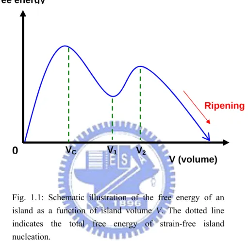
In 1996, S.H. Xin et al. studied the morphology of the CdSe QDs using Atomic Force Microscopy (AFM). Changes in the dot size and the density with time at room temperature were observed. The dot density was observed to drop by an order of magnitude in 10 days, with clear evidence of dot size increased for some dots [8]. After two years, S. Lee et al. further proposed that this behavior of the change in dot size and density with time can be regarded as ripening [9,10]. A systematic investigation of ripening of CdSe self-assembled QDs on ZnSe was reported. They summarized the size and density of the QDs as functions of time after the termination of the deposition of CdSe. As the time increases, the largest QDs continue to grow, the smallest ones quickly disappear, and intermediate dots keep growing as long as there are smaller dots around. When those smaller dots disappear, the intermediate dots become the smallest remaining size, and they are “consumed” eventually by the larger dots. Qualitatively, this behavior is consistent with the predictions of Ostwald ripening: large islands grow by accumulation of material from smaller islands, diffused along the substrate [22,23]. Base on the prediction of Ostwald ripening, if the limiting factor for mass-transfer involves a kinetic surface barrier to the detachment of the atom from the edge of the island, then the dot height is proportional to the cube root of time. Moreover, they also propose that the QDs stability depends on the amount of deposited material, as shown in Fig. 1.1. A surface coverage window exists in which stable (non-ripening) QDs may survive [9]. For surface coverage beyond the window, the QDs undergo morphological changes with time.
On the other hand, I. Daruka and A.L. Barabasi theoretically defined an equilibrium phase diagram for the QD growth mode [24,25]. They investigate the
equilibrium properties of strained heteroepitaxial systems, incorporating the formation and the growth of a wetting layer, dislocation-free island formation, and ripening. The derived phase diagram provides a detailed characterization of the possible growth modes in terms of the island density, equilibrium island size, and wetting layer thickness. The transformation of the growth mode of QD was described as a function of the coverage and the lattice mismatch between QD and buffer. They also concluded that the free energy of the ripened dot decreases monotonically with the increases in dot size; accordingly, a tendency exists to accumulate all available material in an island as large as possible. As a result, some dots grow with time at the cost of other dots. This phenomenon is consistent with the observation of S. Lee et al [9,10]. Similar ripening phenomenon was also investigated in other QD systems, ex. InAs/GaAs, InAs/InP, and GaAs/AlGaAs [26-28]. In this thesis, this ripening effect will be studied in CdSe/ZnSe and ZnTe/ZnSe QD systems.
1.2 CdSe/ZnSe Quantum Dot
CdSe QDs grown on the ZnSe buffer layer constitute one of the most well studied systems among the II-VI compound semiconductors. The lattice constant of ZnSe is almost matched to that of the GaAs substrate and the lattice constant of CdSe is mismatched by about 7% to that of ZnSe buffer layer [29]. Therefore, the CdSe/ZnSe QD system is similar to the InAs/GaAs system, which also exhibits a lattice mismatch of approximately 7% between the InAs QD and the GaAs buffer [30]. The lattice mismatch between InAs and GaAs generates for just enough strain energy to form the QD structures with a wetting layer of about 2.0 MLs under the SK growth mode [31]. The SK growth mode of CdSe/ZnSe QD was also confirmed clearly by AFM images. The thickness of the wetting layer of the CdSe QDs is about 2.5 MLs
[13]. A great deal of effort has been devoted to study the fundamental properties
[32-35] of the CdSe/ZnSe QD structures as well as the potential applications of
incorporating QD structures in laser diodes for emission in the green and blue wavelength range [36].
1.3 ZnTe/ZnSe Quantum Dot
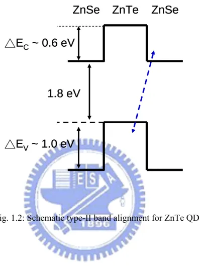
A schematic type-II band alignment for ZnTe/ZnSe QD is shown in Fig. 1.2 using the conduction-band and valence-band offsets of △EC=0.6 eV and △EV =1.0
eV, respectively [37]. The energy from the valence-band edge to the conduction-band edge of the type-II emission is around 1.8 eV. The type-II structure has staggered band structure and spatially separates the electrons and holes. In type-II QD structure, only one species of carriers is confined in the dot, while the other kind of carrier is spread around it by Coulombic attraction between the two different carriers. The spatially separated carriers lead to the appearance of an electric field, which in turn gives rise to the bending of the valence and conduction band (so-called band-bending), and then changes the overlap of the electron and the hole wave-function [38]. Therefore, it has induced much interest cause by the fascinating optical properties and technological applications in photo-detection and photo-voltaic [39-43].
In addition, the existence of non-zero electric dipole moment in type-II QD structures results in the measurable optical Aharonov-Bohm (AB) effect [44-46]. The AB effect in QRs/QDs is predicted to have significant effects upon the luminescence properties, due to the cylindrical symmetry of the confinement, the exciton ground state has zero orbital angular momentum projection (L = 0) at zero magnetic field, but changes to states of higher orbital angular momentum (L = -1, -2, -3) with increasing magnetic field. As a result, the ground state energy oscillates as the L states cross, and the intensity changes from strong (bright excitonic transition with L = 0) to weak (dark excitonic transitions for states with L ≠ 0) with increasing magnetic field
[47,48]. Until now, the AB effects predicted to be observable in the emission have
been seen in both the energy and intensity in a single QD/QR structure. The recent demonstrations of the optical AB effect suggest an interesting possibility to modulate
the emission of QDs, which may have potential applications in quantum information systems [49,50].
1.4 Outline of this Dissertation
The contents of this dissertation surround the ripening dynamics of the self-assembled II-VI semiconductor QDs grown by MBE. Before discussing the experimental results, in Chapter 2, the experimental systems and techniques are introduced. The samples were grown using the Veeco-Applied-EPI 620 and Riber 32P MBE systems. The AFM was employed to measure the sample’s topography. In addition, the optical measurements, including photoluminescence (PL), and time-resolve PL (TR-PL) are presented. At the end of Chapter 2, the RTA technique is also presented.
The main focus of Chapter 3 is the growth dynamics of CdSe/ZnSe QDs. To have an ideal growth condition of QD, in Sec. 3.2, we study the effect of substrate temperatures on the formation of QD. The AFM images reveal that TG is an important
parameter for controlling the dot size. TG must not be too low to ensure that sufficient
kinetic energy is provided for the migration of the CdSe molecules. However, if TG is
too high, the nucleation of the properly sized CdSe QDs becomes difficult. In summary, a TG of 260 oC is the most suitable for further morphology study. In Sec. 3.3,
a complete transfer of the QD growth mode was discussed. As the coverage increases, the growth mode from the FM mode to the SK mode, followed by the ripened mode, was observed in an AFM study. The observations herein are consistent with the theoretical prediction in Ref. 9. The full understanding of growth dynamics is helpful in studying the size control of QD.
The applications of QDs in opto-electronic devices inevitably encounter the problems of the dot density, designed wavelength and size fluctuation. Thus good artificial control during the growth of QDs is an important issue to improve the fabrication of opto-electronic devices with QDs. The ripening dynamics of QDs
provides an additional method for artificial control on the dot density and size. For example, to achieve ultra-low QDs density for the device fabrication which involve with a single QD. In Chapter 4, we investigate the effect of ZnSe partial capping on ripening of CdSe QDs. The final morphology and optical properties of QDs depend on the coverage of the ZnSe partial capping. The mechanism of ripening depending on the thickness of the partial capping layer is discussed in Sec. 4.2. In Sec. 4.3, we presented a model to describe the enhancement factor of ripening, which is an exponential function of the partial capping thickness.
In Chapter 5, we investigate the effect of atomic oxygen on ripening of CdSe QDs. In Sec. 5.2, the results show that atomic oxygen on the surface of ZnSe buffer layer probably change the surface energy and play the role of the nucleation sites. Therefore, the dot density increases and the dot size decreases when the CdSe coverage thickness is kept the same. Moreover, the surface migration of CdSe QDs can be significantly enhanced by introducing the atomic oxygen, and cause the size and the uniformity of QDs to increase during the growth interruption. The results are discussed in Sec. 5.3.
In Chapter 6, the main issue is to study how RTA affects the ripening and band bending of the type-II ZnTe/ZnSe QD structures. The characteristics of as-grown ZnTe/ZnSe QDs with 3.0 MLs are discussed in Sec. 6.2. The average dot diameter and height are 40.5 and 7.86 nm, respectively. The estimated dot density is 1.5 x 109 cm−2. The Stranski-Krastanow growth mode of the ZnTe/ZnSe QDs was verified and
investigated by reflection high-energy electron diffraction (RHEED) and AFM studies. In Sec 6.3, the PL spectra show a significant strong red-shift in the peak energy, when QDs are annealed at an annealing temperature (TA) that exceeds a critical temperature.
It can be well interpreted in terms of the formation of larger QDs by the migration of atoms from the neighboring small QDs, activated by RTA. However, the PL peak
does not exhibit any red-shift as TA is increased further. Moreover, the reduction of
the band-bending effect by RTA was discussed in Sec. 6.4. Based on studies of the time-resolved and excitation power-dependent PL, the observed decreasing of the band-bending effect in the annealed QD could be related to the increase in the dot size.
Reference:
1. M. Shima, Y. Sakuma, Y. Awano, N. Yokoyama, Appl. Phys. Lett. 77, 441 (2000).
2. A.J. Shields, M. P. O’Sullivan, I. Farrer, D. A. Ritchie, R. A. Hogg, M. L. Leadbeater, C. E. Norman, M. Pepper, Appl. Phys. Lett. 76, 3673 (2000).
3. J.C. Kim, H. Rho, L.M. Smith, H. E. Jackson, Appl. Phys. Lett. 73, 3399 (1998). 4. L. Landin, M.S. Miller, M.E. Pistol, C.E. Pryor, L. Samuelson, Science 280, 262
(1998).
5. M. Bayer, O. Stern, P. Hawrylak, S. Fafard, A. Forchel, Nature (London) 405, 923 (2000).
6. R.B. Bylsma, W.M. Becker, J. Kissut, U. Debska, Phys. Rev. B 33, 8207 (1986). 7. J.K. Furdyna, J. Appl. Phys. 64, R29 (1988).
8. S.H. Xin, P.D. Wang, A. Yin, C. Kim, M. Dobrowolska, J.L. Merz, and J.K. Furdyna, Appl. Phys. Lett. 69, 3884 (1996).
9. S. Lee, I. Daruka, C.S. Kim, A.L. Barabási, J.L. Merz, and J.K. Furdyna, Phys. Rev. Lett. 81, 3479 (1998).
10. J.L. Merz, S. Lee, and J.K. Furdyna, J. Crystal Growth 184/185, 228 (1998). 11. P.R. Kratzert, M. Rabe, and F. Henneberger, J. Crystal Growth 166, 332 (2000). 12. D. Litvinov, A. Rosenauer, and D. Gerthsen, Appl. Phys. Lett. 81, 640 (2002). 13. Y.J. Lai, Y.C. Lin, C.P. Fu, C.S. Yang, C.H. Chia, W.K. Chen, D.S. Chuu, W.K.
Chen, M.C. Lee, W.C. Chou, M.C. Chou, and J.S. Wang, J. Crystal Growth 286, 338 (2006).
14. C.S. Yang, J.S. Wang, Y.J. Lai, C.W. Luo, D.S. Chen, Y.T. Shih, S.R. Jian, and W.C. Chou, Nanotechnology 18, 385602 (2007).
15. F. Patella, M. Fanfoni, F. Arciprete, S. Nufris, E. Placidi, and A. Balzarotti, Appl. Phys. Lett. 78, 320 (2001).
16. J.S. Wang, S.H. Yu, Y.R. Lin, H.H. Lin, C.S. Yang, T.T. Chen, Y.F. Chen, G.W. Shu, J.L. Shen, R.S. Hsiao, J.F. Chen, and J.Y. Chi, Nanotechnology 18, 015401 (2007).
17. T. Tawara, S. Tanaka, H. Kumano, and I. Suemune, Appl. Phys. Lett. 75, 235 (1999).
18. Y.G. Kim, Y.S. Joh, J.H. Song, E.D. Sim, K.S. Baek, S.K. Chang, and J.I. Lee, Appl. Phys. Lett. 85, 2056 (2004).
19. D. Guimard,M. Nishioka, S. Tsukamoto, and Y. Arakawa, Appl. Phys. Lett. 89, 183124 (2006).
20. D. Guimard,H. Lee, M. Nishioka, and Y. Arakawa, Appl. Phys. Lett. 92, 163101 (2008).
21. Y.K. Su, S.J. Chang, L.W. Ji, C.S. Chang, L.W. Wu, W.C. Lai, T.H. Fang, and K.T. Lam, Semicond. Sci. Technol. 19, 389 (2004).
22. W. Ostwald, Z. Phys. Chem. (Leipzig) 34, 495 (1990). 23. J. Drucker, Phys. Rev. B 48, 18203 (1993).
24. Daruka, A.L. Barabasi, Phys. Rev. Lett. 79, 3708 (1997). 25. Daruka, A.L. Barabasi, Appl. Phys. Lett. 72, 2102 (1998).
26. E. Dupuy, P. Regreny, Y. Robach, M. Gendry, N. Chauvin, E. Tranvouez, G. Bremond, C. Bru-Chevallier, and G. Patriarche, Appl. Phys. Lett. 89, 123112 (2006).
27. P. Frigeri,L. Nasi, M. Prezioso, L. Seravalli, G. Trevisi, E. Gombia, R. Mosca, F. Germini, C. Bocchi, and S. Franchi, J. Appl. Phys. 102, 083506 (2007).
28. Ch. Heyn, A. Stemmann, A. Schramm, H. Welsch, W. Hansen, and Á. Nemcsics, Phys. Rev. B 76, 075317 (2007).
29. Y. Yang, D.Z. Shen, J.Y. Zhang, X.W. Fan, Z.H. Zhen, X.W. Zhao, D.X. Zhao, Y.N. Liu, J. Cryst. Growth 225, 431 (2001).
30. J.G. Belk, J.L. Sudijono, X.M. Zhang, J.H. Neave, T.S. Jones, B.A. Joyce, Phys. Rev. Lett. 78, 475 (1997).
31. L. Goldstein, F. Glas, J.Y. Marzin, M.N. Charasse, G.L. Roux, Appl. Phys. Lett.
47, 1099 (1985).
32. H. Kirmse, R. Schneider, M. Rabe, W. Neumann, F. Henneberger, Appl. Phys. Lett. 72, 1329 (1998).
33. M. Rabe, M. Lowisch, F. Henneberger, J. Cryst. Growth 184/185, 248 (1998). 34. S.V. Ivanov, A.A. Toropov, S.V. Sorokin, T.V. Shubina, I.V. Sedova, A.A.
Sitnikova, P.S. Kop’ev, Zh.I. Alferov, Appl. Phys. Lett. 74, 498 (1999). 35. N. Matsumura, T. Saito, J. Saraie, J. Cryst. Growth 227/228, 1121 (2001).
36. N.N. Ledentsov, I.L. Krestnikov, M.V. Maximov, S.V. Ivanov, S.L. Sorokin, P.S. Kop’ev, Zh.I. Alferov, D. Bimberg, C.M. Sotomayor Torres, Appl. Phys. Lett.
69, 1343 (1996).
37. Y. Rajakarunanayake et al., J. Vac. Sci. Technol. B 6, 1354 (1988). 38. F. Hatami et al., Phys. Rev. B 57, 4635 (1998).
39. M. Geller, C. Kapteyn, L. Müller-Kirsch, R. Heitz, and D. Bimberg, Appl. Phys. Lett. 82, 2706 (2003).
40. J.R. Madureira, M.P.F. de Godoy, M.J.S.P. Brasil, and F. Iikawa, Appl. Phys. Lett. 90, 212105 (2007).
41. D.A. Alvarez, B. Alen, J.M. Garcia, and J.M. Ripalda, Appl. Phys. Lett. 91, 263103 (2007).
42. J. Tatebayashi, A. Khoshakhlagh, S.H. Huang, L.R. Dawson, G. Balakrishnan, and D.L. Huffaker, Appl. Phys. Lett. 89, 203116 (2006).
and D. Huffaker, Appl. Phys. Lett. 90, 173125 (2007).
44. I.R. Sellers, V.R. Whiteside, I.L. Kuskovsky, A.O. Govorov, and B.D. McCombe, Phys. Rev. Lett. 100, 136405 (2008).
45. I.R. Sellers, V.R. Whiteside, A.O. Govorov, W.C. Fan, W.C. Chou, I. Khan, A. Petrou, and B.D. McCombe, Phys. Rev. B 77, 241302 (2008).
46. E. Ribeiro, A.O. Govorov, W. Carvalho, and G.M. Ribeiro, Phys. Rev. Lett. 92, 126402 (2004).
47. A.V. Kalameitsev, A.O. Govorov, and V.M. Kovalev, JETP Lett. 68, 669 (1998). 48. A.O. Govorov, S.E. Ulloa, K. Karrai, and R.J. Warburton, Phys. Rev. B 66,
081309 (2002).
49. E. Knill, R. LaFlamme, and G. Milburn, Nature (London) 409, 46 (2001).
50. N. Gisin, G. Ribordy, W. Tittel, and H. Zbinden, Rev. Mod. Phys. 74, 145 (2002).
Free energy
0
V (volume)
Ripening
VC V1 V2
Fig. 1.1: Schematic illustration of the free energy of an island as a function of island volume V. The dotted line indicates the total free energy of strain-free island nucleation.
ZnSe
ZnTe
ZnSe
△E
C~ 0.6 eV
1.8 eV
△E
V~ 1.0 eV
ZnSe
ZnTe
ZnSe
△E
C~ 0.6 eV
1.8 eV
△E
V~ 1.0 eV
Chapter 2. Experiments and Techniques
In this chapter, we will introduce the experimental systems and techniques, including the molecular beam epitaxy (MBE), atomic force microscopy (AFM), photoluminescence (PL), time-resolved photoluminescence (TR-PL), and rapid thermal annealing (RTA) treatment.
2.1 Molecular Beam Epitaxy (MBE)
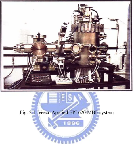
MBE is a technique for epitaxial growth via the interaction of one or several molecular or atomic beams that occurs on a surface of a heated crystalline substrate. The samples, which were studied in this dissertation, were grown using the Veeco-Applied-EPI 620 or Riber 32P MBE systems. The Veeco Applied EPI 620 MBE system is shown in Fig. 2.1, which is a six-source vertical growth chamber. It includes the vacuum systems, analytical equipments, one introduction chamber, and one growth chamber.
The growth chamber contains all of the components and analytical equipment. Currently, we have five cells, which contain materials Zinc (Zn), Selemium (Se), Cadmium (Cd), Manganese (Mn), and Tellurium (Te). An Addon RF-plasma source with independently separated pumping design which could provide very abrupt oxygen incorporation for supplying reactive atomic oxygen (O) radicals. The flux of oxygen gas is controlled by a mass flow controller system. The EPI 40 cc low temperature cells are used for the evaporation of the elemental solid source Zn, Te, Cd, and Se. For Mn Solid source, the EPI 40 cc standard temperature cell is used. Each of the cells has its own shutters to control the growth time. There is a main-shutter
between sources and substrate to protect substrate from evaporation before growth. The common focus of the cells is at the sample plane on a substrate heating stage, which can be continuously rotated for highly uniform growth. Substrate motion is imparted to the manipulator’s magnetically coupled drive train from a servomotor. The reflection high-energy electron diffraction (RHEED) system is also set up in the growth chamber. It is an invaluable tool to determine different aspects of the depositing layer. Morphological information of the surface may be interpreted from the spot and line patterns typical on the displayed phosphor screen during growth.
To maintain the low growth chamber pressure required for molecular beam epitaxy, the Veeco Applied EPI620 MBE system uses several kinds of pumps. Both the growth and introduction chambers are roughly pumped (the range between atmosphere and approximately 100 mtorr) using an oil-free mechanical diaphragm pump. The introduction chamber uses the Varian V-250 turbo-molecular pump to reduce the pressure to the high vacuum region (<5×10⁻⁸ torr ) in all volumes. The growth chamber uses a single cryogenic pump, which is a closed loop liquid He cryogenic pumping system, to reach high vacuum, and ultrahigh vacuum (<1×10⁻¹⁰ torr).
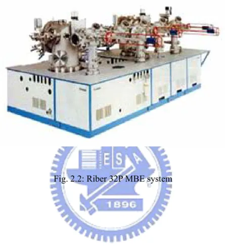
The another MBE systems: Riber 32P is shown in Fig. 2.2, which has eight materials sources, include Mg, Zn, Se, Te, Cd, ZnS, ZnCl2, and RF generated nitrogen. The samples of ZnTe/ZnSe type-II QDs for studying the effect of RTA on the ripening and the band-bending effect were grown using this MBE system.
The detailed growth procedures of the sample structures were described in the first section of each corresponding chapters.
2.2 Atomic Force Microscopy (AFM)
Binnig, Quate, and Gerber invented the AFM in 1985. Their original AFM consisted of a diamond shard attached to a strip of gold foil. The diamond tip contacted the surface directly, with the interatomic van der Waals forces providing the interaction mechanism. The AFM was developed to overcome a basic drawback with STM, that it can only image the surfaces of conductor or semiconductor. The AFM, however, has the advantage of imaging almost any type of surface, including polymers, ceramics, composites, glass, and biological samples.
In this dissertation, the NT-MDT SOLVER P47 AFM was used for the morphology study. The schematic diagram of the AFM system is shown in Fig. 2.3. The measurement was carried out using the semi-contact mode. The scan step in x, y direction are both 4.8 nm. The resolution is 0.01 nm in the z direction. The shape of silicon tip is conic. Its diameter and height are 30 and 70 nm (i.e. the aspect ratio, α= H/D= 7/3), respectively. The aspect ratio of silicon tip is much lager than that of the CdSe QD (typical aspect ratio of CdSe QD is about 4.3×10⁻²) grown in current study. Therefore, no further treatment on the AFM data is needed.
2.3 Photoluminescence (PL)
PL is a process in which a substance absorbs photons and then re-radiates photons. It can be described as an excitation to a higher energy state and then a return to a lower energy state accompanied by the emission of a photon. This is one of many forms of luminescence and is distinguished by photoexcitation. The period between absorption and emission is typically shorter than 1 ns or maybe as long as several hundred ns. PL is an important technique for measuring the purity and crystalline quality of semiconductor.
The experimental setup for PL measurements is shown in Fig. 2.4. The samples were loaded on the cold finger of a closed-cycle refrigerator. The 325 nm line of a He-Cd laser was employed to excite the PL spectra. A Spex-1403 double-grating spectrometer, equipped with a thermal electric cooled photomultiplier tube, was used to analyze the PL spectra. The slit widths were set to 100 m to yield a spectral resolution of better than 0.1 meV. High spectrum resolution which is better than 0.1 meV can be obtained.
2.4 Time-resolved Photoluminescence (TR-PL)
The recombination dynamics of the samples were studied by TR-PL. A pulsed diode laser (375 nm) with a repetition rate of 2.5 MHz is employed as the excited source for TR-PL measurements. The decay traces are recorded using the time-correlated single photon counting technique with an overall time resolution of ~120 ps.
2.5 Rapid Thermal Annealing (RTA)
RTA is an alternative to conventional furnace annealing. Its advantages include short annealing time and precise control of the annealing profile. Thermally induced intermixing in such QD systems has attracted considerable attention as a way of tuning or controlling the emission properties of the QD assemblies [1-6].Typically, a blue-shift of the peak energy is observed concurrently with a narrowing of the peak linewidth after RTA [1-3].
In this dissertation, the ZnTe/ZnSe type-II QDs were treated with RTA in pure N2
environment. RTA process was performed using tungsten-halogen lamps at temperatures from 300 to 480 °C. The rising and cooling rate of temperature is about 30 °C/sec, and the annealing time is fixed at 30 sec.
Reference:
1 R. Leon, Y. Kim, C. Jagadish, M. Gal, J. Zou, and D. J. H. Cockayne, Appl. Phys. Lett. 69, 1888 (1996).
2 S. Malik, C. Roberts, R. Murray, and M. Pate, Appl. Phys. Lett. 71, 1987(1997). 3 S. J. Xu, X. C. Wang, S. J. Chua, C. H. Wang, W. J. Fan, J. Jiang, and X. G. Xie,
Appl. Phys. Lett. 72, 3335 (1998).
4 D. Bhattacharyya, A. Saher Helmy, A. C. Bryce, E. A. Avrutin, and J. H. Marsh, J. Appl. Phys. 88, 4619 (2000).
5 R. Leon, S. Fafard, P. G. Piva, S. Ruvimov, and Z. L.-Weber, Phys. Rev. B 58, R4262 (1998).
6 A. Babiński, J. Jasiński, R. Boźek, A. Szepieiow, and J. M. Baranowski, Appl. Phys. Lett. 79, 2576 (2001).
Fig. 2.4: Experimental setup for the PL measurement
Argon - ion
Laser
L1
L2
L3
TRIAX550
Singal-Grating
Spectrometer
Computer
PMT Closed Refrigerator 1.71.81.92.02.12.22.32.42.5 15K PL In te ns ity (a .u .)Photon Energy (eV) ZnTe
Chapter 3. Growth Dynamics of CdSe
Self-Assembled Quantum Dots
In this chapter, the growth dynamics and optical properties of CdSe/ZnSe quantum dots (QDs) will be discussed. The self-assembled CdSe/ZnSe QDs were grown at various growth temperatures on GaAs (001) by molecular beam epitaxy. Experimental results indicated an optimum growth temperature was found to be 260
oC. The Stranski–Krastanow (SK) growth mode was confirmed clearly by atomic
force microscopy images. The thickness of the wetting layer of the CdSe QDs is about 2.5 mono-layers (MLs). Two types of QDs were found with the CdSe coverage of 3.0 MLs. As the coverage increases, a complete transfer of the QD growth mode from the Frank van der Merve (FM) mode to the SK mode, followed by the ripened mode, was observed in an AFM study. A schematic diagram of the growth mechanism of self-assembled CdSe QDs is presented. Moreover, the photoluminescence spectra of samples with various thicknesses were investigated. A dramatic change of optical properties confirmed that the QD structure formed with thickness above 2.5 MLs [1].
3.1 Growth of CdSe/ZnSe Quantum Dots
Self-assembled CdSe QDs were grown on a ZnSe buffer layer using Veeco Applied EPI 620 MBE system. The ZnSe buffer layer was grown on the epi-ready GaAs substrate. Before growth, the GaAs surface was cleaned by chemical etching with H2O : NH4OH : H2O2 in the ratio 50 : 5 : 5 for 2 minutes, followed by rinsing
with D.I. water and final drying with nitrogen gas. The time between chemical etching and the transfer of the substrate into the vacuum chamber is less than 5 minutes. The
substrate temperature (TG) was then raised to 650 oC to desorb the residual oxide on
the GaAs surface. Desorption process was monitored by a reflection high energy electron diffraction (RHEED) pattern. After desorption, TG was decreased to 350 oC
to grow the ZnSe buffer layer. The ZnSe buffer layer includes several MLs grown by migration enhance epitaxy (MEE) [2], and a thickness of 20 nm grown by the conventional MBE growth mode. The average roughness of the ZnSe buffer layer is about 0.28 nm. After the flat ZnSe buffer layer was deposited, the growth of the self-assembled CdSe QDs began. Table 3.1 presents the uncapping sample parameters in the AFM study. Samples 1, 2 and 3 have the same average coverage of CdSe (3.0 MLs), but the values of TG were 240, 260 and 280 oC, respectively. The TG values of
samples 4 to 7 are fixed at 260 oC. The average coverage of CdSe for samples 5 to 7 are between 2.0 and 3.0 MLs. Sample 4 was grown without CdSe coverage to investigate the roughness of ZnSe buffer. The average coverage of CdSe was determined by the growth duration and the growth rate, which was calibrated by a thick CdSe epilayer whose growth conditions were the same as those of QDs. The growth rate was determined by measuring the growth duration and the thickness of the thick CdSe epilayer. The thickness was estimated from the energy spacing of the interference peaks of the reflectivity spectrum. The thickness of the CdSe layer was further verified by optical microscopy with a resolution of 0.1μm. For a CdSe epilayer with a thickness of 1μm and accuracy of 0.1μm, the uncertainty of the growth rate is about 10%. It implies the accuracy of the CdSe coverage is about 10%, i.e. the uncertainty is less than several tenths MLs for the CdSe coverage of 2 to 4 MLs. Determining the thickness of the wetting layer is crucial. The thickness of the ZnSe buffer layers is 20 nm. Above the ZnSe buffer layer, CdSe was grown with an average coverage fixed at 3.0 MLs. Buried dots were also prepared for optical studies. The growth condition of the samples for the optical study was the same as that of
3.2 Optimum Growth Temperatures
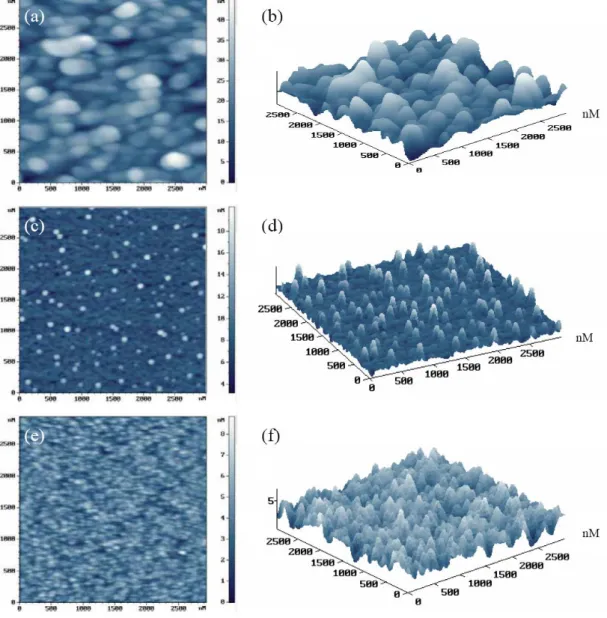
Figures 3.1(a)/3.1(b), Figs. 3.1(c)/3.1(d) and Figs. 3.1(e)/3.1(f) show the plane view/3D view of AFM for sample 1 (TG = 240 oC), sample 2 (TG = 260 oC) and
sample 3 (TG = 280 oC), respectively. The vertical axis labeled with black and white
contrast is drawn at the right-hand side of the plane views to represent the height of a QD. In Figs. 3.1(a) and 3.1(b), large islands are observed. The average diameter and height of the large islands are about 291 and 29.81 nm, respectively. The dots are large and their sizes are not uniform. As TG is increased slightly for sample 2,
self-assembled CdSe QDs form, as depicted in Figs. 3.1(c) and 3.1(d). The QDs are divided into a group of large dots (H > 4 nm) and one of small dots (H < 4 nm). The average diameter of the larger (smaller) dots is approximately 86 (66) nm and the mean height is 5.35 (2.21) nm. The dot density of both groups is approximately 20.0×108 cm-2. The dot density increased abruptly as TG is increased further for
sample 3, as shown in Figs. 3.1(e) and 3.1(f). The dots are very close to each other. As a result, some dots were connected. Random dot shapes are observed. Also, the size distribution is very broad. This sample is less useful for further study. The above result reveals that TG is an important parameter for controling the dot size. TG must
not be too low to ensure that sufficient kinetic energy is provided for the migration of the CdSe molecules. However, if TG is too high, the nucleation of the properly sized
CdSe QDs becomes difficult. In summary, a TG of 260 oC of sample 2 is the most
3.3 Growth Mode Transfer
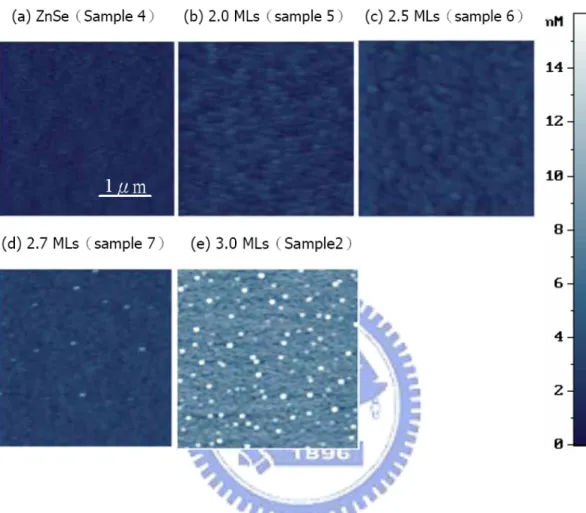
Figure 3.2 shows the plane view of AFM for samples 2, 4, 5, 6, and 7. At both ends of the axis, the black and white represent the lowest point at 0 nm and the highest point at 16 nm. In Fig. 3.2(a), the weak black and white contrast indicates the smooth surface of the ZnSe buffer layer. The average roughness of the ZnSe surface is less than 0.28 nm. When the average CdSe coverage was 2.0 MLs (sample 5), the average surface roughness changed from 0.28 to 0.42 nm. No clear 3D island formation is observed in Fig. 3.2(b). When the average coverage was further increased to 2.5 MLs (sample 6), the QD structures still could not be observed but the surface roughness increased slightly to 0.45 nm. The only change associated with the increase in the CdSe coverage from 2.0 to 2.5 MLs is the roughing of the sample surface. As the average coverage increased further to 2.7 MLs (sample 7), as shown in Fig. 3.2(d), the 3D dots began to appear. The dot density of sample 7 is 2.0×108 cm-2. The average dot height and diameter are 2.95 and 68.3 nm, respectively. And the average aspect ratio, α= H/D, is 4.3×10⁻². This aspect ratio is much smaller than that (α= 0.25) measured using the amplitude scan of the taping mode by K. Kitamura et al. [3] The dot density is ten times lower too. However, the above observation indicates that the critical thickness is between 2.5 to 2.7 MLs for the transition of 2D to 3D growth, i.e. the thickness of the wetting layer is about 2.5 to 2.7 MLs. Reference 15 reported the similar result.
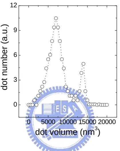
In Fig. 3.2(e), the average coverage is 3.0 MLs (sample 2) and two groups of QD were observed. The average diameter and height of the larger (smaller) dots are 86 (66) and 5.35 (2.21) nm, respectively. The dot density of the larger (smaller) dots is 15.2×10⁸ (4.8×10⁸) cm-2. The dot size distribution (the number of dots versus the dot volume) of sample 2 was summaried in Fig. 3.3. The dot volume was calculated based
on the assumption that the dots are conical. The two group size distributions were observed. The coexistence of small and large dots is similar to that in the second ripen (R2) growth mode, which is theoretically defined by I. Daruka and A.L. Barabasi [4, 5], as shown in the equilibrium phase diagram of Fig. 3.4. Figure 3.4 refers to phase diagram II in Ref. 5. It was obtained by minimizing the sum of the energy of the strained overlayer, the free energy of the QDs and the total energy density of the ripened islands. The x-axis represents the misfit between the buffer layer and the material grown above. While the y-axis represents the average coverage of QD. For a very small misfit and low coverage, only the 2D layer-by-layer growth mode, i.e. the FM mode, is allowed. For a misfit that is less than but close to 0.065, the growth mode starts with the FM mode. If the average coverage is above 3.0 MLs, a ripened (R1) growth mode begins. For misfit between 0.069 and 0.075, the growth starts with
the FM mode and proceeds to the SK1 mode and then to the R2 mode as the coverage
increases. In the SK1 growth mode, the 3D QDs were grown on the wetting layer. In
the R2 growth mode, the larger ripened QDs and the smaller coherent SK QDs coexist.
In current study, the misfit between the ZnSe buffer layer and the CdSe QD is about 0.07, as indicated by the dotted line in Fig. 3.4. The equilibrium phases of the Volmer-Weber (VW), SK2 and R3 growth modes are not discussed herein, since in this
work, the misfit is less than 0.1.
To summarize the above investigation, a schematic growth dynamics is shown in Fig. 3.5. Figures 3.5(a) to (c), which correspond to CdSe coverages of 0, 2.5 and 2.7 MLs, respectively, indicate the SK growth mode of CdSe QDs. In Fig. 3.5(d), the CdSe coverage was 3.0 MLs; the original smaller QDs grow into larger ripened QDs, while some smaller SK dots appeared in the flat spaces to relax the remaining stress. As a result, the growth mode changed form the SK mode to the R2 growth mode, as
observed at TG = 260 oC with the average CdSe coverage from 2.5 to 3.0 MLs. Figure
3.2(e) clearly shows the ripen growth state for a CdSe coverage from 3.0 to 3.5 MLs, which is also schematically demonstrated in Fig. 3.5(d).
In addition to the above characterization by AFM, PL studies were also performed. The PL spectra for several samples with the CdSe coverage of 1.0 MLs to 3.3 MLs were obtained at 10 K, as shown in Fig. 3.6(a). The peak position clearly shifts toward lower energy as the CdSe coverage increases. Figure 3.6(b) presents the dependence of the PL peak position on the CdSe coverage. Two linear dependences were found. The abrupt change in the slope is about 2.5 MLs, which value is consistent with the thickness of the CdSe QD’s wetting layer, observed by the AFM studies. Restated, when the CdSe coverage was less than the thickness of the wetting layer, no 3D dots were formed. The dependence of PL peak position on CdSe coverage follows a linear behavior contributed by the 2D quantum well. The high PL peak energy, which is very close to the 2.812 eV value of the bulk ZnSe energy gap, can be attributed to the effect of inter-diffusion, energy shift due to strain and the confinement energy of the 2D quantum well. When the CdSe coverage exceeded the thickness of the wetting layer (2.5 MLs), the QD structure formed. The dependence of PL peak position on CdSe coverage obeys another linear relation. The PL transition energy of QDs decreases as the dot size increases. This statement was verified by temperature-dependent PL spectra. Figure 3.7 plots the activation energy (Ea) versus
the CdSe coverage. Ea was obtained form the following equation
)] / exp( 1 /[ ) 0 ( ) ( 0 0 T I D E kT I a , (3.1),
where )I0(T and I0(0) are the integrated PL intensities at temperatures T and 10 K, respectively. D is a fitting parameter, and k is the Boltzmann constant. In Fig. 3.8, curves A and B are fitting using equation (3.1) for 2.0 and 2.7 MLs samples, respectively. Ea increased steeply when the CdSe coverage was near 2.5 MLs. This
finding supports the QD morphology obtained by AFM and the study of the dependence of the PL peak position on the CdSe coverage mentioned above. Below 2.5 MLs, the exciton transition energy is close to the band gap of the ZnSe barrier. As a result, the activation energy which to dissociate the exciton from the CdSe 2D quantum well into the ZnSe barrier is small. As the CdSe coverage increases, the increased thickness of 2D quantum well will reduce the confinement of carriers. Therefore, the activation energy decreases with the CdSe coverage increases as the coverage less than 2.5 MLs. In addition, 2.5 MLs, 3D QDs were formed. Ea increases
abruptly because the exciton binding energy in QDs is much strong. A further increase in CdSe coverage reduces Ea because the exciton binding energy decreases as the dot
size increases. The fitting curve B initially increases and then decrease as the temperature rises. This behavior is typical of QDs [6-8]. Fitting curve A decreases rapidly as the temperature ruses, indicating 2D quantum well behavior.
3.4 Summary
Self-assembled CdSe QDs were grown on the ZnSe buffer layer. The optimum growth temperature was found to be 260 oC. The thickness of the wetting layer of the CdSe QDs is between 2.5 and 2.7 MLs. Two types of QDs were observed when the average CdSe coverage was 3.0 MLs. The change in the growth mode from the SK mode to the R2 growth mode was confirmed. A schematic diagram of growth
dynamics of self-assembled CdSe QDs was presented. A dramatic change in the optical property verifies that the thickness of the wetting layer of the CdSe QDs is about 2.5 MLs, which result is consistent with the result of AFM studies.
Reference:
1. Y.J. Lai, Y.C. Lin, C.B. Fu, C.S. Yang, C.H. Chia, D.S. Chuu, W.K. Chen, M.C. Lee, W.C. Chou, M.C. Kuo and J.S. Wang, J. Cryst. Growth 286, 338 (2006). 2. K. Leonardi, H. Heinke, K. Ohkawa, D. Hommel, H. Selke, F. Gindele, U.
Woggon, Appl. Phys. Lett. 71, (2000) 1510.
3. K. Kitamura, H. Umeya, A. Jia, M. Shimotomai, Y. Kato, M. Kobayashi, A. Yoshikawa, K. Takahashi, J. Cryst. Growth 214/215, (2000) 680.
4. I. Daruka, A.L. Barabasi, Phys. Rev. Lett. 79 (1997) 3708. 5. I. Daruka, A.L. Barabasi, Appl. Phys. Lett. 72, (1998) 2102.
6. N. Matsumura, T. Saito, J. Saraie, J. Cryst. Growth 227/228, (2001) 1121.
7. G. Karczewski, S. Mackowski, M. Kutrowski, T. Wojtowicz, J. Kossut, Appl. Phys. Lett. 74, (1999) 3011.
8. M. Funato, A. Balocchi, C. Bradford, K.A. Prior, and B.C. Cavenett, Appl. Phys. Lett. 80, (2002) 443.
Table 3.1: Growth parameters of samples for studying the growth dynamics of CdSe self-assembled quantum dots.
Fig. 3.1: AFM plane view and three-dimensional view for 3.0 MLs CdSe QD samples 1 (TG = 240 oC), 2 (TG = 260 oC) and 3
Fig. 3.2: AFM plane view for CdSe QDs with the coverage from 0 to 3.0 MLs.
0
5000 10000 15000 20000
0
3
6
9
12
dot
number
(
a.
u.
)
dot volume (nm
3)
Fig. 3.3: Dot size distributions of sample 2 (3.0 MLs). The dot volume was calculated by assuming the dots are conical. The two group size distributions were observed.
Fig. 3.4: Equilibrium phase diagram of the self-assembled QDs, obtained by minimizing the sum of the energy of the strained overlayer, the free energy of the QDs and the total energy density of the ripened islands. The x-axis is the misfit between the buffer layer and the material grown above. The y-axis represents the average coverage of QD.
Fig. 3.5: Schematic diagram of the growth dynamics for the self-assembled CdSe QDs: (a) to (c) SK growth mode, (d) R2 growth
mode, showing coexisting larger ripened QDs and smaller coherent QDs.
2.5 2.6 2.7 2.8 2.3 MLs (a) 1.0 ML 2.0 MLs 2.7 MLs 3.3 MLs In te n s it y ( a .u .)
Photon Energy (eV)
Fig. 3.6: (a) PL spectra from capped CdSe QDs for various coverages. The CdSe coverage increases from 1.0 to 3.3 MLs. (b) PL peak position depends on the CdSe coverage, and two slopes are observed.
1 2 3 4 0 20 40 60 80 100 120 140
Ac
tiv
a
tio
n
e
n
e
rg
y
(
m
e
V
)
CdSe coverage (ML)
Fig. 3.8: Lines A and B represent the PL intensity of CdSe QDs with coverages of 2.0 MLs and 2.7 MLs, respectively. Line A indicates the behavior of quantum well, and line B is typical of QDs.
0
50
100
150
200
250
In
te
nsity
(a
.u
.)
Temperature (K)
A B
Chapter 4. Effect of ZnSe Partial Capping on
the Ripening of CdSe QDs
In this chapter, we investigate the ripening dynamics of CdSe quantum dots (QDs) covered with several MLs of the ZnSe capping layers. The final morphology and optical properties depend on the coverage of the ZnSe partial capping. The mechanism of ripening depending on the thickness of the partial capping layer is discussed. Our model indicates that the enhancement factor of ripening is an exponential function of the partial capping thickness [1].
4.1 Sample Growth
The CdSe/ZnSe QDs were grown on GaAs (001) substrates at 260 oC by molecular beam epitaxy (MBE). After the growth of QDs, a subsequent interruption of 2 minutes at 260 oC allowed the ripening of QDs to proceed. Following the 2 minutes interruption, a thin ZnSe capping layer, which is thinner than the dot height (so-called partial capping), was deposited. Finally, a 2 minutes annealing process was carried out at the same temperature to proceed the enhanced ripening. Then, the sample was immediately cooled and removed from the MBE chamber. For photoluminescence (PL) measurements, a 50 nm-thick ZnSe layer was deposited on top of the ZnSe partial capping layer.
4.2 Enhancement of Ripening by Partial Capping
Figure 4.1(a) shows the morphology of a representative CdSe QD from the uncapped sample. The diameter, D=79.5 nm, and height, H=6.81 nm, of the QDs were the average of several scans from different areas. In chapter 2, we confirmed this QD formation in ripening (R2) mode. The size and density of the three-dimensional dots
change with time. Figures 4.1(b) to 4.1(d) show AFM images of the representative CdSe QDs capped with ZnSe layers of various thicknesses from 1 to 3 MLs. Notably, the dot size increased from Figs. 4.1(a) to 4.1(d), and the aspect ratios for the QDs partially capped with different ZnSe coverages are similar. Table 4.1 summarizes the average size and density of the partially capped and uncapped dots. The dot height/density increases/declines as the thickness of the ZnSe partial capping layer increases, revealing that a large amount of mass transportation occurs after the ZnSe partial capping was deposited. The dot transformation is very sensitive to the thickness of the partial capping from 1 to 3 MLs, indicating that the ripening rate of partially capped dots exceeds that of uncapped dots. Namely, the ripening rate of CdSe QDs is significantly enhanced by the ZnSe partial capping at 260 oC.
In Fig. 4.2, the dot height (H) was analyzed as a function of the in-chamber annealing time (t) using the theory of Ostwald ripening to elucidate further the dynamics of the observed ripening effect. At t = 0, the deposition of CdSe QDs was just completed. From t = 0 to 2 minutes, the QDs undergo the ripening process. ZnSe partial capping layers of various thicknesses were deposited at t = 2 minutes to accelerate ripening. This process took only about 10 s, depending on the thickness of ZnSe partial capping. The sample was maintained at 260 oC for 2 minutes (from t = 2 to 4 minutes) to undergo enhanced ripening before it was cooled to perform AFM measurements. The Ostwald ripening predicts that if the limiting factor for
mass-transfer involves a kinetic surface barrier to the detachment of the atom from the edge of the island, then H(t) ~ t1/3[2,3]. For CdSe QDs without in-chamber annealing, the average dot height at t = 0 is about H0 = 5.4 nm. Curve A describes the ripening
process of CdSe QD without ZnSe capping for t = 0 to 2 minutes. Curve A connects H(t=0) =H0=5.4 nm to H(t=2) = 6.8 nm. The equation for curve A is
3 / 1 0 0 ) (t H V t H (4.1), where V0 corresponds to the ripening rate of the uncapped QDs.
Consider the enhancement in the ripening rate due to the presence of the partially capped ZnSe layer. Curve B in Fig. 4.2 represents the enhanced ripening of CdSe QDs with a 2 MLs-thick ZnSe partial capping, given that the ZnSe partial capping was completed at t = 0. The equation for curve B is
H(t)H0 Vt1/3 (4.2),
where V corresponds to the ripening rate of partially capped QDs. However, in this work, the ZnSe partial capping layer was deposited 2 minutes after QD formation. Therefore, the equation describes the increase in the dot height after the deposition of ZnSe partial capping (t = 2~4) should be modified as
3 / 1 3 0 )] 2 2 ( [ ) ( H V t t H (4.3),
where is an enhancement factor, defined by =V/V0. The term
) 2 2 ( 3 denotes the difference between the times required on curves A and B for the dot height from H0 increases to 6.8 nm. Curve C plots Eq. (4.3) for t = 2 to 4, which was obtained by
shifting curve B by ) 2 2 ( 3
. Consequently, the variation of dot height could be completely described by the solid line in Fig. 4.2. The ripening rates for the samples that were partially capped with ZnSe layer of 1 and 3 MLs were 1.5V0 and 3.8V0,
Figure 4.3 displays the PL spectra of samples with ZnSe partial capping coverage of various thicknesses at 10K. The samples with partial capping with a thickness of below 3 MLs exhibit a strong red-shift, revealing that the dot size increases with the coverage of partial capping. However, when the coverage of partial capping exceeds 4 MLs, only a small red-shift occurs in the PL peak energy. If the QDs are covered with a thick capping layer, then atomic migration will be significantly suppressed, and the ripening rate is substantially reduced [4]. Therefore, the red-shifts in samples e (4 MLs) and f (7 MLs) are less than that of sample d (3 MLs). As the coverage of partial capping further increases to 20 MLs (sample g), the ripening process is fully suppressed by the existence of thick capping layer. Hence, the peak energy of sample g is very close to that of the uncapped sample a, as shown in Fig. 4.3.
4.3 Effect of the Partial Capping Thickness
The rates of atomic detachment and attachment are governed by the energy barrier at the edge of the ripened quantum dots. Strain lowers the energy barrier for atomic diffusion [5]. As a result, the increasing thickness of partial capping raises the strain energy and accelerates the ripening. Therefore, the ripening rate of QDs can be artificially controlled by tuning the strain energy through thickness manipulation of capping layer. The strain energy () can be related to the coverage of capping layer (n) by ) exp( ) ( ) ( n k n i f i (4.4), where k is a fitting parameter which corresponds to the degree of dependence of on n. Without ZnSe partial capping (n=0), the strain energy of QDs is i. The strain
energy increases with the coverage of the capping layer. However, it converges to a limiting value f at high coverage of partial capping. An exponential function that is
similar to Eq. (4.4) is applied to fit the dependence of the enhancement factor on the coverage of partial capping, as shown in Fig. 4.4. The results could be fitted very well by ) exp( 1 ) ( n n (4.5), whereand are the fitting parameters. Equation (4.5) describes a strong increase in the enhancement factor at low partial capping coverage, and agrees nicely with the presented results. However, for partial capping that exceeds a thickness of 4 MLs, atomic migration for the ripening process is significantly suppressed by cap layer, making ripening more complicated than is out of our assumption and discussion.
4.4 Summary
We performed AFM and PL studies of a series of CdSe QDs with partially capped ZnSe layers of various coverages. The AFM images offer clear evidence that the coverage of partial capping is important to ripening. The enhancement factor of ripening is an exponential function of the partial capping coverage. Furthermore, the PL measurement corroborates the AFM study. These results strongly support the fact that ZnSe partial capping enhances the ripening of CdSe quantum dots.
Reference:
1. Y.J. Lai, C.S. Yang, W.K. Chen, M.C. Lee, W.H. Chang, W. C. Chou, J. S. Wang, W. J. Huang, and Erik S. Jeng, Appl. Phys. Lett. 90, 83116 (2007).
2. S. Lee, I. Daruka, C.S. Kim, A.L. Barabási, J.L. Merz, J.K. Furdyna, Phys. Rev. Lett. 81, 3479 (1998).
3. W. Ostwald, Z. Phys. Chem. (Leipzig) 34, 495 (1990).
4. S.H. Xin, P.D. Wang, A. Yin, C. Kim, M. Dobrowolska, J.L. Merz, and J.K. Furdyna, Appl. Phys. Lett. 69, 3884 (1996).
Table 4.1: Size and density of the uncapped and partially capped CdSe QDs obtained from AFM images.