國立交通大學
電子工程學系 電子研究所
碩 士 論 文
馬西森定則在金氧半場效電晶體電子通用
遷移率造成的誤差並其修正
The Error of Matthiessen’s Rule in MOSFET electron
Universal Mobility and Its Correction
研究生: 黃怡惠 Yi-Hui Huang
指導教授: 陳明哲 博士 Prof. Ming-Jer Chen
馬西森定則在金氧半場效電晶體電子通用
遷移率造成的誤差並其修正
The Error of Matthiessen’s Rule in MOSFET electron
Universal Mobility and Its Correction
研究生: 黃怡惠 Yi-Hui Huang
指導教授: 陳明哲 博士 Prof. Ming-Jer Chen
國立交通大學
電子工程學系 電子研究所
碩士論文
A Thesis
Submitted to Department of Electronics Engineering & Institute of Electronics
College of Electrical and Computer Engineering National Chiao Tung University
in Partial Fulfillment of the Requirements for the Degree of
Master of Science in
Electronics Engineering October 2012
Hsinchu, Taiwan, Republic of China
I
馬西森定則在金氧半場效電晶體電子通用
遷移率造成的誤差並其修正
研究生: 黃怡惠 指導教授: 陳明哲 博士
國立交通大學
電子工程學系 電子研究所碩士班
摘要
本篇論文主旨係分析利用馬西森定則計算使用平面場效電晶體量子模擬器 模擬得到的電子通用遷移率與使用馬西森定則計算萃取的電子通用遷移率之間 的誤差。此研究方法主要專注於高電場區域,通用的遷移率含有兩種不同的散射 機制(1)聲子散射所造成的遷移率與(2)表面粗糙度散射所造成的遷移率。通過實 驗驗證組成的自洽求解薛丁格方程式與卜松方程式以及通用遷移率的模擬程式 的使用,我們嘗試修正使用馬西森定則來求得金氧半場效電晶體的遷移率所造成 的實驗誤差。而此修正過的定則的核心在於物理的半經驗模型,並且可以使用最 低能帶的佔有率與各個遷移率的組成來明確表示使用傳統馬西森定則所造成的 誤差。此新的模型可以在實際的條件下成立(溫度高達 400K)並且可應用在廣泛 的基底摻雜濃度(1014 to 1018 cm-3)。另外,也可以延伸應用到 500MPa 單軸拉應 力下。II
The Error of Matthiessen’s Rule in MOSFET electron
Universal Mobility and Its Correction
Student: Yi-Hui Huang Advisor: Dr. Ming-Jer Chen
Department of Electronics Engineering and Institute of Electronics
National Chiao Tung University
Abstract
An analysis of the errors caused by Matthiessen’s rule between the apparent universal mobility which is calculated by Matthiessen’s rule and the simulated universal mobility curves are presented in this thesis. To focus on the high surface field region, the universal mobility features two distinct scattering mechanisms: one of phonon alone and one of surface roughness alone. By means of the experimentally-validated simulation package consisting of a self-consistent solving of Schrődinger and Poisson’s equations and a universal mobility simulation program, we try to correct the experimental error of applying Matthiessen’s rule to MOSFET mobility universality. Thus, the aim of this work is to devise an error-free version of Matthiessen’s rule. The core of the new rule lies in a physically- based semi-empirical model, which explicitly expresses the errors due to the conventional use of Matthiessen’s rule as a function of both the lowest subband population and the relative strength of individual mobility components. The new model holds under practical conditions (with temperatures up to 400 K) and in a broad range of substrate doping concentrations (1014to 1018cm-3). Extension to the case of strain is also presented in terms of a uniaxial tensile stress of 500 MPa.
III
Acknowledgements
在碩士的求學中,我由另一間大學的研究所轉換到一個新環境,其實感到相 當的恐懼與不安。非常感謝陳明哲教授在這些日子以來教導並指引我,讓我漸漸 的熟識這個充滿溫暖的環境,並且在我遇到挫折時給予我方向,讓學生能夠得到 勇氣努力地前進。此外,也相當的感謝博士班的李韋漢學長總是有耐心教導我, 讓我得知自己的不足以及應該要努力的方向。感謝我們 309A 實驗室的學長、學 姊、同學以及學弟妹們,謝謝你們陪伴我一同走過這些日子。另外還要再次感謝 陳宛勵同學與葉婷銜同學,是你們讓我在這些奮鬥的日子裡多了一份歡樂,也學 習到了許多事情。最後我要感謝一路上陪伴著我,為我擔心受怕的父母以及兄長, 我有你們的支持才有勇氣走到這裡,並且努力認真地走下去,謝謝你們!IV
Contents
Chinese Abstract……….….………I English Abstract……….……….II Acknowledgements………...………... III Contents………... IV Figure Captions……….V Table Captions……….IX Chapter 1 Introduction………...…………. 1Chapter 2 Physical Theory for Quantum Simulator NEP………... 3
2.1 Schrődinger and Poisson Self-consistent “NEP” in n-MOSFETs……… 3
Chapter 3 Electron Mobility Model………... 7
3.1 Introduction………... 7
3.2 Phonon Scattering Mechanism………. 8
3.3 Surface Roughness Scattering Mechanism……….. 10
3.4 Derivation of Two-Dimensional Mobility in the Universal Mobility Region…12 3.5 Coulomb Scattering Mobility Model with Ionized Impurities in Substrate Region……… 13
3.6 The Effective Electron Mobility Calculated by Matthiessen’s Rule………… 15
Chapter 4 Result and Discussion……… 18
4.1 Introduction………. 18
4.2 The Model of the Error Produced by Matthiessen’s Rule………... 18
4.3 Correction Model of Matthiessen’s Rule………... 22
Chapter 5 Conclusion……….. 24
V
Figure Captions
Figure 2.1 The energy band diagram of a poly gate/SiO2/p-substrate system... 27
Figure 2.2 The flowchart of Poisson and Schrödinger self-consistent solving procedure.……….28
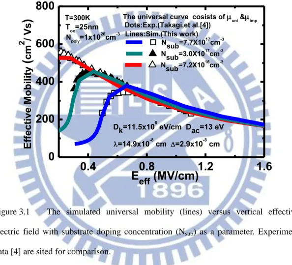
Figure 3.1 The simulated universal mobility (lines) versus vertical effective electric field with substrate doping concentration (Nsub) as a parameter. ……….29
Figure 3.2 The simulated universal mobility (lines) versus different definitions of vertical effective electric field with substrate doping concentration (Nsub) as a parameter in surface roughness’s model: (a). The experimentally empirical formula. (b). The vertical electric field defined in Eq.(3.1.1) [11]. ………30
Figure 3.3 The comparison of the data (symbol) [6] and ionized impurity limited mobility curves by simulated (blue line) and be extracted by Matthiessen’s rule (red line) versus different substrate doping concentrations for an inversion layer Ninv=1012 cm-2 at 300 K.………31
Figure 3.4 Calculated the error Er,imp (lines) which be defined in Eq. (3.6.4) versus inversion layer concentration for six different substrate doping
concentrations (1015 to 1018 cm-3) at 300 K.……….32
Figure 3.5 The error Er,imp defined in Eq. (3.6.4) versus substrate doping
concentration for an inversion density and to simulations with Fig. 3. in [6] ……….33
Figure 4.1 Comparison of simulated electron total mobility (lines) with the
experimental one (symbols) [10] versus vertical effective electric field with Δ = 2.9Å and λ =14.9 Å for (a) six substrate concentrations and
VI
(b) four temperatures of 397K, 342K, 242K, and 297K. ………34
Figure 4.2 Simulated universal mobility, phonon limited mobility, and surface roughness limited mobility (lines with symbols) versus Eeff for
Nsub = 1017 cm-3 at 300K. The apparent universal mobility (lines) obtained by Matthiessen’s rule and hence the errors are together plotted. The arrow indicates the critical Eeff where phonon and surface
roughness limited mobilities have the same value. The inset shows corresponding population of two lowest subbands. ……….……35
Figure 4.3 The apparent universal mobility (lines) obtained by Matthiessen’s rule, simulated universal mobility, phonon limited mobility, and surface roughness limited mobility (lines with symbols) versus Eeff for (a)
Nsub= 5×1017cm-3, (b) Nsub= 1017cm-3, (c) Nsub= 1016cm-3, (d) Nsub = 1015 cm-3, and (e) Nsub = 1014 cm-3 at 300K. The arrow indicates the critical Eeffwhere phonon and surface roughness limited mobilities have the same value. The inset shows corresponding population of two lowest subbands...………36
Figure 4.4 The universal mobility (lines) obtained by Matthiessen’s rule, simulated
universal mobility, phonon and surface roughness limited mobilities
(lines with symbols) versus Eeff for (a) Nsub =1018 cm-3,
(b) Nsub = 5×1017 cm-3, (c) Nsub = 1017 cm-3, (d) Nsub = 1016 cm-3,
(e) Nsub = 1015 cm-3, and (f) Nsub = 1014 cm-3 at 200K. The arrow
indicates the Eeff where phonon and surface roughness limited
mobilities have the same value. The inset shows corresponding population of two lowest subbands..………39
VII
Figure 4.5 The universal mobility (lines) obtained by Matthiessen’s rule, simulated universal mobility, phonon and surface roughness limited mobilities (lines with symbols) versus Eeff for (a) Nsub =1017cm-3, (b)
Nsub = 1016cm-3, (c) Nsub = 1015cm-3, and (d) Nsub = 1014cm-3 at 100K.
The arrow indicates the Eeff where phonon and surface roughness
limited mobilities have the same value. The inset shows corresponding population of two lowest subbands.………42
Figure 4.6 Electron effective mobility data (symbols) [10] for five substrate doping concentrations at 300K versus vertical effective electric field Eeff. Simulated universal mobility curves (lines) are shown. Dac is the acoustic deformation potential; Dk is the deformation potential of the k-th intervalley phonon; is the surface roughness correlation length;
and is the surface roughness rms height.………...……44
Figure 4.7 Scatter plot (symbols) of the simulated peak error and corresponding lowest subband population, created from different substrate doping concentrations (1014 cm-3 to 1018 cm-3), with temperature as a parameter. The calculated results (dashed lines) using Eq. (4.2.4) are shown.….45
Figure 4.8 Extracted (symbols) pre-factor
a
in Eq.(4.2.4) versus temperature. The best fitting (dashed line) is shown………46Figure 4.9 Fitted temperature (symbols) power-law exponent γ in Eq.(4.2.4) versus temperature. The best fitting (dashed line) is shown………….47
Figure 4.10 Comparison of simulated (symbols) and calculated (lines) errors for
five different substrate doping concentrations at 300 K, plotted as a function of the ratio of phonon limited mobility and surface roughness
VIII
limited mobility………48
Figure 4.11 The total mobility (lines) obtained by Matthiessen’s rule, simulated
total mobility, phonon and surface roughness limited mobilities (lines with symbols) versus Eeff for (a) Nsub =1018 cm-3, (b) Nsub = 5×1017 cm-3
, (c) Nsub = 1017 cm-3, (d) Nsub = 1016 cm-3, and (e) Nsub = 1015 cm-3 at 300K. The arrow indicates the Eeff where phonon and surface
roughness limited mobilities have the same value. The inset shows corresponding population of two lowest subbands………...49
Figure 4.12 Scatter plot (symbols) of the simulated peak error Er,max and the peak error Er,tot (hollow squares) versus corresponding lowest subband population, created from different substrate doping concentrations (1015
cm-3 to 1018 cm-3) at 300K………...….52
Figure 4.13 Scatter plot (symbols) corresponding to Figure 4.7 but under a uniaxial
tensile stress of 500 MPa. The calculation results (dashed lines) came from Eq. (4.2.4) with the pre-factor a =-0.018+ 2.6910-4T and the
power-law exponent = 1/(0.042 - 910-4
IX
Table Captions
Table I Electron scattering and physical parameters for Si used in this work and
1
Chapter 1
Introduction
As we know, the mobility in the inversion layers of nMOSFETs can be limited to three primary scattering mechanisms: ones is the surface roughness scattering at SiO2/Si substrate interface; second is the acoustic/optical phonon scattering in inversion channel region; and the final mechanism is the Coulomb impurity scattering due to the ionized impurity atoms in substrate depletion region.
Because of its additive property of reciprocal mobility components, Matthiessen’s rule in principle may be a useful tool to probe individual scattering mechanisms in the inversion layers of nMOSFETs. It has been pointed out earlier by Stern [1] that the errors due to the use of Matthiessen’s rule will be more than 15% for temperatures over 40K. Since then, there have been four fundamentally different methods concerning the validity and applicability of Matthiessen’s rule [2]-[7] as published in the literature. First, Matthiessen’s rule must be carried out under the extreme or impractical conditions such as very low temperatures (near absolute zero) [2]. Second, sophisticated numerical simulations on individual mobility components with no need to account for Matthiessen’s rule [3] were used instead. Third, while assessing mobility components individually [4], [5], the errors caused by Matthiessen’s rule were overlooked for the engineering purpose. Fourth, mobility simulations were performed to deliver the errors of mobility components extracted with the rule [3], [6], [7]. On the other hand, the current understanding of the error of Matthiessen’s rule has been significantly improved.
In this thesis, we propose a new method in terms of an error-free version of Matthiessen’s rule. This method is demonstrated in the universal mobility region and
2
takes the practical situations into account. The merit of the method is that it can correct the error of Matthiessen’s rule and thereby ensure the applicability of the rule. Importantly, Stern [1] suggested the relative strength of individual mobility components as one origin of the errors. The other origin in terms of the subband population was put forward by Fischetti, et al. [3]. The establishment of the method in this work is closely linked to these two origins.
3
Chapter 2
Physical Theory for Quantum Simulator NEP
2.1 Schrődinger and Poisson Self-consistent “NEP” in
n-MOSFETs
Self-consistent fully solving of Poisson and Schrődinger’s equations in n-channel MOSFETs (metal-oxide-semiconductor field-effect transistors) [10] is introduced in terms of our Nano Electronics Physics “NEP” simulator.
The time-independent Schrödinger equation in the quantum mechanics can be expressed in terms of a matrix equation:
2 2
2m V E
(2.1) Eq.(2.1) can be written as a general differential equation by the finite element method: 2 1 1 2 ( ) 2 ( ) ( ) [ ] ( ) ( ) ( ) 2 i i i i i i x x x V x x E x m x (2.2) n n n a
(2.3)where is the wave-function which be assumed that it is confined in a small region of Wq. Here Wq includes the entire inversion region. Generally, the wave-function
dividing this region into n intervals of the equal-distance x Wq/n can be expanded by an orthogonal basis set
n . Eventually, we solve the self-consistent Poisson and Schrődinger equations by Newton’s method. Thus, the simulating results would contain the n eigen-values (En) corresponding to the n wave-function (
n). The4
excited states.
We give the schematic energy band diagram and physical environmental setup in Figure 2.1. The band diagram of silicon substrate along the out-of-plane direction is separated into two parts: one is the surface quantum confinement region (𝑊𝑞𝑢𝑎𝑛𝑡𝑢𝑚) and the other is the bulk classical region (𝑊𝑐𝑙𝑎𝑠𝑠𝑖𝑐𝑎𝑙).
In the former region, the carriers are confined in this shallow region, where we meshed 300 intervals of width dz0 0.2 nm to make sure the simulation accuracy. In the later region, we adopt the conventional formula; that is, (𝑊𝑐𝑙𝑎𝑠𝑠𝑖𝑐𝑎𝑙) isdivided
into 100 intervals with a width of 𝑑𝑧1 =𝑊𝑐𝑙𝑎𝑠𝑠𝑖𝑐𝑎𝑙100 . It can significantly reduce the computational time but not lose the accuracy. Additionally, the conduction band edge at the interface is set to be zero of energy in n-MOSFETs.
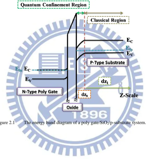
The common self-consistent step with the flowchart is illustrated in Figure 2.2. Firstly, we guessed the surface band bending Vs into the Poisson equation with the
boundary conditions V (z=0) =Vs and V (z=bulk) =0. Then, it would obtain the corresponding initial potential profile V(z), thus along with V(z) to calculate 1D Schrődinger equation, as revealed in Eq.(2.1).
We can obtain the eigen-values and the wave-function as been mentioned in the
previous paragraph. Moreover, we summarize the basic formulation and the iteration procedure we use to perform a self-consistent solution. In the surface quantum confinement region, the three-dimensional carriers in terms of electrons density 𝑛3𝐷(z) and holes density 𝑝3𝐷(𝑧) can be described by
, 2 3 , 2 , , ( ) ( ) ( ) ( ) i j D i j D i j i j E n z DOS E f E dE z
5 , ( ) 2 , 2 , ln 1+e ( ) f i j E E i DOS kT i B i j i j m g k T z
(2.4) , 2 3 , 2 , , ( ) ( ) (1 ( )) ( ) u j E D u j D u j u j p z DOS E f E dE z
, ( ) 2 , 2 , ln 1+e ( ) u j f E E u DOS kT u B u j u j m g k T z
(2.5)where i and u are the electron valley index and the hole valley index, respectively. j is the subband index, and gi and gu are the degeneracy of the ith valley and uth valley, respectively; miDOS and mDOSu are the density of states electron and hole effective mass, and Ei,j and Eu,j are the electron and hole energy levels. The corresponding
wave-functions i j, and u j, are all normalized. The carrier density in the bulk classical region is given by:
1/ 2 2 ( ) ( ) C V z n z N F kT (2.6) 1/ 2 2 ( ) ( ) V V z p z N F kT (2.7) where Nc and Nc are the conduction-band density of states and valence-band density
of states, and F1/2 is the Fermi-Dirac interal. Substituting these into the 1-D Poisson
equation, we obtain 2 [ ( ) ( ) ( )] ( ) d si e N z n z p z d V z dz (2.8) where Nd( )z
is the ionized donor density. Ultimately, we can get a new potential V(z) to satisfy Eq.(2.8) and use Newton’s method to iterate the step continuously until the final potential profile V(z) is obtained, within a tolerable error. The two-dimensional electron density can be described as
6 , , 2 ln 1+e f i j E E i DOS kT i j i B m n g k T (2.9)
and the total inversion layer charge density is given as
, ,
inv i j
i j
N
n (2.10).The average inversion layer thickness Zav is written as
2 , , , 0 ( ) bulk i j av i j i j s n Z z z dz N
(2.11)The potential calculation for the high doping poly-silicon gate situation is demonstrated as: 2 ln( ploy sub) fb B i N N V k T n (2.12) where Vfb is the flat band voltage, kB is the Boltzmann’s constant, Npoly is the poly gate
concentration, Nsub is the substrate doping concentration and ni is the intrinsic
concentration. The poly gate voltage and oxide voltage are shown below:
2 2 Si s poly poly F V eN (2.13) ox Si s ox ox t F V (2.14) where toxis the oxide thickness, si and
ox are the dielectric constant of the silicon and oxide, respectively, and the surface electric field is given by(z 1) (z 2) s V V F z
. Finally, the total gate voltage can be expressed as
g s ox poly fb
V V V V V
(2.15) where Vs indicates the surface band bending determined by the potential profile in the silicon substrate.
7
Chapter 3
Electron Mobility Model
3.1 Introduction
In this section, we use the sub-band energy and the wave function provided by our NEP simulator to calculate the universal electron mobility under the relaxation time approximation. Then, we obtain corresponding mobility by only considering lowest four subbands in twofold valleys and two subbands in fourfold valleys.
In addition, we discussed the momentum relaxation rates caused by scattering with phonons and surface roughness which can be considered the expression of the universal mobility curve.
We also quoted the detailed model in a textbook by Lundstrom [9] to deal with the Coulomb scattering with ionized impurities in substrate of n-type polysilicon gate (n-polygate) to compare with the calculated ionized impurity mobility extracted by using Matthiessen’s rule. Validity of Matthiessen’s rule will be addressed in Chapter 4 as well. Figure 3.1 illustrates that the calculated universal electron mobility is insensitive to the substrate concentrations or process parameters when plotted as a function of high effective field (E ). In addition, eff Eeff can be defined via the empirical formula: 0 ( inv dep) eff si e N N E (3.1.1) where is taken as 0.5. We determined the inversion carrier concentration (Ninv)
and the surface concentration of the depletion charge (Ndep) by NEP. Eventually, all of the scattering parameters used in this work are listed on Table I.
8
3.2 Phonon Scattering Mechanism
As we all know, lattice vibrations will deform the crystal deformation potential, perturbing the dipole moment between atoms, and causing the degradation of inversion layer mobility due to the pressure waves which result from the lattice vibrations.
The mechanisms of phonon scattering can be classified into the acoustic phonon scattering and optical phonon scattering; acoustic phonon scattering displaces nearby atoms in the same directions and optical phonon scattering displaces adjacent atoms in opposite directions. Acoustic phonon energy is smaller than carrier energy while the kth intervalley f-type phonon energy Ek(f) is 59 meV, and the kth intervalley g-type phonon energy Ek(g) is 63meV according to the phase of the vibration with the two different atoms in one primitive cell.
Intravalley phonon scattering only considers acoustic phonons, thus according to Takagi, et al. [10], the momentum-relaxation rateacm n, ( )E from the mh subband to the nth subband is written as:
2 1 (2 / 4) (2 / 4) 2 2 , 2 , 3 (2 / 4) , 1 1 , ( ) ( ) ac v d ac B m n m n m n ac l m n n m D k T W z z dz W s
(3.2.1)where the index of (2/4) in acm n,(2 / 4) represents twofold valleys and fourfold valleys,
respectively, 2 ac v n (=2)and 4 ac v
n (=1) are the degeneracy of the twofold valleys and fourfold valleys with regard to intravalley scattering, respectively. Dac (=13 eV)
means the deformation potential due to acoustic phonons, is the crystal density,
l
s is the longitudinal sound velocity, Wm n, is the form factor decided by the wave-functions of the 𝑚-th subband and the n-th subbands, which expresses the
9
interaction’s effective thickness in the z-direction. It is the main difference of the 2D and 3D cases. kB is the Boltzmann constant, and is the Planck constant divided by
2π. The total scattering rate in the mth subband is decided by summing up acm n, within
all the subbands where can be written as
, (2 / 4) (2 / 4) ( ) 1 ( ) ( ) m m m n n ac ac U E E E E
(3.2.2)where U x( )
1(x0) and 0(x0)
is a step function.For intervalley phonon scattering, the momentum-relaxation rate INTERm n, ( )E from mth subband in twofold valleys to the nth subband in fourfold subband, according
to Takagi, et al. [13], can be written as
2 { } 2 4 4 , ' 2 , 1 ( ) 1 1 1 1 ( ) ( ) 2 2 2 1 ( ) f f n d k k k k n m n k INTER k m n n m D f E E N U E E E E E W f E
(3.2.3)
, 1 ' 2 ' 2 ( ) ( ) m n m n W
z z dz (3.2.4)where nnf24(=4) indicates the degeneracy of the valleys for intervalley scattering,
4
d
m is density-of-states effective mass of the final state (fourfold valley), E and k D k are the deformation energy and potential for the kth intervalley phonon. In addition, “+”
means phonons emission and “ - ” means phonons absorption in the signs
1 1 2 2 k N
, andN signifying the occupation number of the kk th intervalley phonon is
defined as 1 [exp( ) 1] k k B N E k T (3.2.5)
In the same way, the relaxation time , 4'( )
m n
INTER E
from mth subband in fourfold valleys
into the nth subband in twofold subband, and , 4( )
m n
INTER E
10
fourfold valleys into the nth subband in fourfold subband are described as
2 { } 4 2 2 ' , 4 , 1 ( ) 1 1 1 1 ( ) '( ) 2 2 2 1 ( ) f f n d k k k k n m n k INTER k m n n m D f E E N U E E E E E W f E
(3.2.6)
2 { } 4 4 4 ' , ' 4 , 2 { } 4 4 4 ' ' , 1 ( ) 1 1 1 1 ( ) ( ) 2 2 2 1 ( ) 1 ( ) 1 1 1 ( ) 2 2 2 1 ( ) f f n d k k k k n m n k INTER k m n g g n d k k k k n k k m n n m D f E E N U E E E E E W f E n m D f E E N U E E E E W f E
(3.2.7)
1 ' 2 2 , ( ) ( ) m n m n W
z z dz (3.2.8) where 4 2 f n n (=2), 4 4 g n n (=1), and 4 4 f nn (=2) are the degeneracy of the intervalley phonon scattering, respectively.
3.3 Surface Roughness Scattering Mechanism
The roughness scattering at the interface of Si/SiO2 is very important for a MOSFET device at high fields, resulting in the degradation of mobility in the inversion layer. There are usually two kinds of assumptions involved in the analysis of mobility, one is the exponential autocovariance function and the other is Gaussian autocovariance function.
We prefer using the Gaussian autocovariance function in this work because the surface roughness scattering rate calculated by exponential model needs larger values of the root mean square amplitude Δ to fit the mobility data of experimental than the Gaussian model.
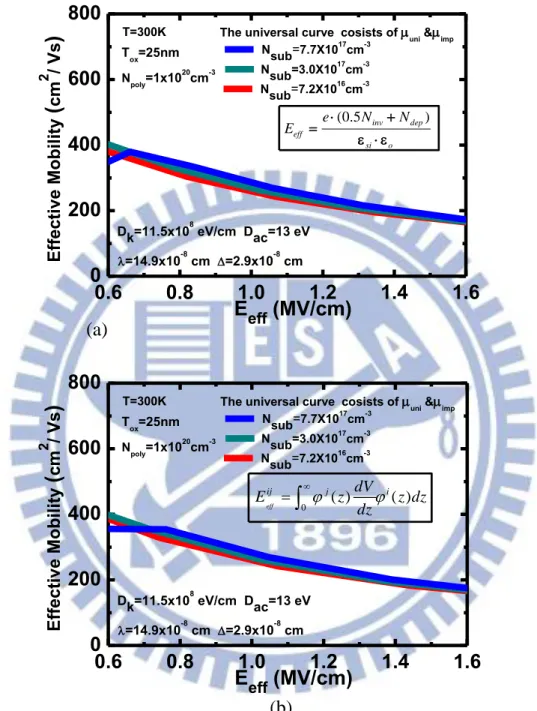
Moreover, we need to make an important assumption that the approximation of single subband is quite accurate. We only consider the intrasubband scattering although surface roughness is anisotropic scattering. Due to Yamakawa, et al.’s surface roughness model [11] , the scattering rate for a Gaussian function is described
11 as 2 2 ( ) 2 2 2 2 2 4 , 3 0 ( ) 1 ( ) (1 cos ) ( ) 2 DOS eff j ij q j i j SR m E e E U E E e d E
(3.3.1)Assuming the elastic collisions without energy transition, Eq. (3.3.1) can be rewrite as 2 2 2 2 ( ) 2 2 2 2 2 sin 2 2 , 3 0 ( ) 1 ( ) 2sin ( ) 2 2 j DOS eff m E E j ij j i j SR m E e E U E E e d E
(3.3.2) 2 2 2 2 =2 (1 cos ) =4 sin 2 q k k (3.3.3) ( ) 2 2 2 (E-E ) = DOS j j m k (3.3.4) where ( ) DOS jm and Ej are the density of states effective mass and the electron subband energy in the jth subband, and 𝜆 is the correlation length. In addition, in order to
obtain universal mobility curves more accurately,
eff
ij
E can be presented by a new definition [11] in place of the empirical formula via Eq.(3.1.1). The compared results are described in Figure 3.2. The new definition of
eff ij E is given as 0 ( ) ( ) eff ij j dV i E z z dz dz
(3.3.5) where eff ijE is the electron effective field from the ith subband to the jth subband,
( )
i
z
and j( )z are the wave-functions of the initial and final states of the electrons, respectively.
12
3.4 Derivation of Two-Dimensional Mobility in the
Universal Mobility Region
In this work, we can express the total scattering rates of the twofold and fourfold valley in terms of the phonon scattering and surface roughness scattering for ith
subband with the energy (E) as [10]:
2 2 2 1 1 1 ( ) ( ) ( ) i i i phonon SR E E E (3.4.1) 4 4 4 1 1 1 ( ) ( ) ( ) i i i phonon SR E E E
(3.4.2)for ith subband of twofold and fourfold valleys, respectively. Then, the electron
mobility
2i and
4i in ith subband of twofold and fourfold valleys by using theaverage energy within the 2DEG in the relaxation time approximation can be given as
0 2 2 2 ( ) ( )( ) ( )( ) i i i i E i c E i f q E E E dE E f m E E dE E
(3.4.3) ' ' 4 4 ' 4 ( ) ( )( ) ( )( ) i i i i E i c E i f e E E E dE E f m E E dE E
(3.4.4)where mc2 and mc4 are the conductivity effective masses in two- and fourfold valleys,
respectively. f is Fermi-Dirac distribution function. Eventually, we averaged over the subband occupation to obtain total universal mobility
uni, as described by' 2 4 ' ' ( i i i i ) i i uni s N N N
(3.4.5)13
3.5 Coulomb Scattering Mobility Model with Ionized
Impurities in Substrate Region
The Coulomb scattering due to ionized impurity atoms in the substrate region results in the degradation of mobility at lower field. In this section, we use an analytical model derived elsewhere [9] to calculate ionized impurity mobility. The perturbing potential is the screened Coulomb potential [9], [12], as
2 exp( / ) 4 s D o si e U r L r (3.5.1) 2 0 si o B D k T L e n (3.5.2)
where r is the distance from the scattering center, L is the Debye length. D o is the
permittivity of free space , and siis the permittivity of the semiconductor (Si). n0 is
the 3-D density of the mobile carrier.
Then the scattering rate of Coulomb scattering due to ionized impurity in 3-D case can be presented by
3 4 2 2 2 2 2 2 1 [ln(1 ) ] ( ) 16 2 1 I imp o si N e r r E E m r
(3.5.3) 2 2 2 2 2 8 4 ( ) D D mEL p r L (3.5.4)where N is the ionized impurity concentration, However, Eq.(3.5.3) is not the 2-D I
electron gas inside the MOSFET, and our simulator is used for the two-dimensional inversion layers, thus the scattering rate of Coulomb scattering due to ionized impurity should be given in 2-D case.
14
three-dimensional case at the scattering process of 2-D carriers should be replaced by the integral as 2 2 2 2D 3D ( z) z H
H I q dq (3.5.5) ( ) ( ) ( ) ( ) iq zz z mn z m n I q I q
z z e dz (3.5.6) where 𝐻2𝐷 and 𝐻3𝐷 are the matrix elements for two dimensions and threedimensions scattering, respectively. However, |𝐼𝑚𝑛|2 is the form factor given by the wave-functions of the 𝑚-th subband and the n-th subbands, and it can be written as
,
m n
W -1 which have be mentioned in section 3.2. Therefore, the scattering rate of ionized impurity scattering in 2-D case from mth subband to nth subband can be
expressed as 3 4 2 2 2 2 , 2 2 2 , 2 / 4 3 , ( ) 1 1 [ln(1 ) ] ( ) 16 2 1 ( ) I D m n imp o si D m n N e r g E r E E m r g E W
(3.5.7)where g2D( )E and g3D( )E are the density of states for two dimensions and three dimensions scattering, respectively. It should be noticed that only intrasubband scattering is considered.
According to [12], we letthe Debye length of Eq.(3.5.2) to be rewritten as
0 2 ox av B D inv Z k T L e N (3.5.8)
whereNinvand Z are the average 2-D inversion charge density and thickness of av inversion layer which have be mentioned in Section.2.1 and can be calculated by NEP simulator.
Besides, the calculated total electron mobility including the influence on ionized impurity scattering mechanisms can be treated as mentioned in section 3.4. The total
15
scattering rates of the twofold and fourfold valley in terms of the phonon scattering, surface roughness scattering and ionized impurity scattering for ith subband with the
energy (E) can be described as [10]:
2 2 2 2 1 1 1 1 ( ) ( ) ( ) ( ) i i i i phonon SR imp E E E E (3.5.9) 4 4 4 4 1 1 1 1 ( ) ( ) ( ) ( ) i i i i phonon SR imp E E E E
(3.5.10)for ith subband of twofold and fourfold valleys, respectively. And the electron mobility
2
i
and
4i in ith subband of twofold and fourfold valleys can be defined as2 2 2 ( ) ( )( ) ( )( ) i i i i E i c E i f e E E E dE E f m E E dE E
(3.5.11) ' ' 4 4 ' 4 ( ) ( )( ) ( )( ) i i i i E i c i E f e E E E dE E f m E E dE E
(3.5.12)Finally, we can acquire the total universal mobility
tot containing the influence on ionized impurity scattering mechanisms by the averaging over the subband occupation as ' 2 4 ' ' ( i i i i ) i i tot s N N N
(3.5.13)3.6 The Effective Electron Mobility Calculated by
Matthiessen’s Rule
16
our simulator, 𝜇𝑢𝑛𝑖,𝑀 is the apparent universal mobility in combination with phonon mobility and surface roughness mobility at high field. It can be defined based on Matthiessen’s rule as follows:
,
1
1
1
uni M ph sr
(3.6.1) Besides, 𝜇𝑡𝑜𝑡,𝑀 is the total mobility which is constructed by phonon mobility,surface roughness mobility, and ionized impurity mobility according to Matthiessen’s rule: , 1 1 1 1 tot M ph sr imp
(3.6.2) Besides, 𝜇𝑖𝑚𝑝,𝑀 is the mobility for ionized impurity mobility mechanism extracted with Matthiessen rule, as given by,
1
1
1
imp M tot uni
(3.6.3)
Refer to D.Esseni, et al.[5], we can compare 𝜇𝑖𝑚𝑝,𝑀 and 𝜇𝑖𝑚𝑝 by the
error 𝐸𝑟,𝑖𝑚𝑝 produced by Matthiessen’s rule as , , imp M imp r imp imp
E
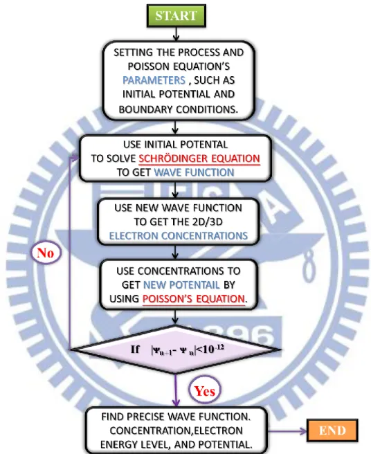
(3.6.4) Figure 3.3 shows 𝜇𝑖𝑚𝑝,𝑀 and 𝜇𝑖𝑚𝑝 for an inversion density Ninv 1012cm 2
versus different substrate doping concentrations at 300 K. As we can see, the values of corresponding mobility are close to the simulation results of D.Esseni, et al.[5].
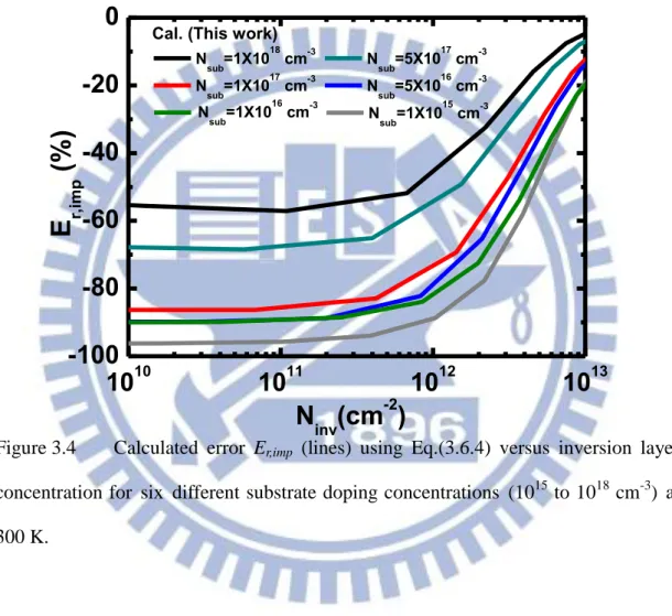
Besides, the error Er,imp which be defined in Eq. (3.6.4) calculated with six different
substrate concentrations (1015 to 1018 cm-3) versus inversion layer concentration are shown in Figure 3.4. Eventually, the resulting error 𝐸𝑟,𝑖𝑚𝑝 versus substrate doping concentration Nsub for an inversion density Ninv 1012cm2 is presented in
17
Figure 3.5, and the outcomes conform to Fig. 3 of [5] well. As shown, we can observe a discrepancy between 𝜇𝑖𝑚𝑝,𝑀 and 𝜇𝑖𝑚𝑝. This error is quite large. It is demonstrated that ionized impurity mobility extracted by Matthiessen’s rule should not be regarded as experimental data.
18
Chapter 4
Result and Discussion
4.1 Introduction
In this section, the resulting total mobility, consisting of phonon limited mobility, surface roughness limited mobility, and ionized impurity mobility, was found to reproduce experimental data [10] well for different substrate concentrations and different temperatures (T=397K, 342K, 242K, 297K). This was obtained for root mean square height of the surface roughness amplitude (Δ) of 2.9 Å and a correlation length of the surface roughness (λ) of 14.9 Å , which are mentioned in section 3.3. The result is also compared with Takagi et al.[10] as depicted in Figure 4.1.It can be seen that the larger the substrate doping concentration 𝑠𝑢 , the narrower the range of the vertical effective electric field Eeff dominated by phonon and surface roughness
scatterings.
The validity of Matthiessen’s rule has been known to be not exact for a long time. In this work, we show that the mobility extraction by using Matthiessen’s rule would overestimate the value of experimental data. What’s more, we analyze the accuracy of Matthiessen’s rule and propose a simplified model for errors, finding the relationship with the errors between different substrate doping concentrations.
4.2 Model of the Error Produced by Matthiessen’s Rule
Using the aforementioned parameters, the apparent universal mobility (𝜇𝑢𝑛𝑖,𝑀) calculated by Matthiessen’s rule, the simulated universal curves (𝜇𝑢𝑛𝑖), phonon
19
limited mobility, surface roughness limited mobility and the errors Er between 𝜇𝑢𝑛𝑖,𝑀 and 𝜇𝑢𝑛𝑖versus Eeff are plotted in Figure 4.2for 𝑠𝑢 =1018cm-3at 300K. The inset in
Figure 4.2 shows the corresponding population of two lowest subbands. The errors Er
between 𝜇𝑢𝑛𝑖,𝑀 and 𝜇𝑢𝑛𝑖 can be defined as
, uni M uni r uni E (4.2.1) However, we calculated the universal mobility and the corresponding error
quantitatively by the compared method are given below,
1 1 1 uni phonon SR (4.2.2)
where 𝜇𝑢𝑛𝑖,𝑀 have been defined in Eq. (3.6.1).
Remarkably, we found that the largest errors occur at a critical Eeff where
phonon limited mobilityis equal to surface roughness limited mobility and apart from this point the errors decrease gradually, as shown in Figure 4.2. This indicates the relative strength of phononlimited and surface roughness limited mobility [1]. The population of subband i of valley j can be defined as pij, and come from the other origin [3], the twofold lowest subband population po which also be described as p11
can be drawn under
ph=
sr as shown in the inset of Figure 4.2.The comparison results with other substrate doping concentration s (1014 to 1017 cm-3) and different temperatures (100 to 300K) are shown in Figure 4.3 to Figure 4.5. These figures pointed out that Matthiessen’s rule overestimates the extracted universal mobility. Specifically, the maximum error of universal mobility caused by using Matthiessen’s rule is below 30%.
Note that the critical Eeff is larger than 1 MV/cm in Figure 4.2 and far away from
the Coulomb scattering region due to ionized impurity as experimentally shown in Figure 4.6.
20
A scatter plot between the peak of error Er,max and the corresponding twofold
lowest subband population po (under ph
=
sr) for different substrate dopingconcentrations (1014 to 1018 cm-3) with temperature as a parameter is shown in Figure 4.7. Because the separation of subband is strong with high doping
concentration, more inversion carrier occupies on lowest subband with high doping concentration and low temperature. We found that the peak of error Er,max increase for
increasing temperatures and decreasing substrate doping concentrations. Obviously, there is a unique relationship existing. We can figure out a power-law relationship between the two:
,max r o
E
ap
(4.2.3)where a is the pre-factor and is the power-law exponent. In Figure 4.8 we show different temperatures corresponding to different values of a, and different temperatures corresponding to different values of as depicted in Figure 4.9.
However, there is a fitting line that can be drawn in Figure 4.8 and Figure 4.9, yielding a =0.024 + 2.4910-4 T and = 1/ (0.026 910-4 T) in Figure 4.8 and Figure 4.9, respectively, regardless of the doping concentrations.
At this point, we are able to establish a semi-empirical model in the context of the relative strength of ph and sr :
,max min( , ) (1 exp( )) max( , ) ph sr r r ph sr E E (4.2.4)
Through best fitting, we obtained = -5 and = 1 and 2 for ph < sr and
ph > sr, respectively. The validity of the error calculated by Eq.(4.2.3) and Eq.(4.2.4)
has been confirmed by the simulation for different substrate doping concentrations (1014 to 1018 cm-3) at 300 K
.
The left hand side of Figure 4.10reveals21
such results for fivedifferent substrate doping concentrations at 300 K as ph < sr,
and the results for ph > sr as shown in the right hand side of Figure 4.10. Note that
under the critical situation of ph =sr, Er in Eq. (4.2.4) reduces to its peak value Er,max.
Finally, we want to highlight that the validity of the errors Er between 𝜇𝑢𝑛𝑖 and 𝜇𝑢𝑛𝑖,𝑀 which did not consider the mobility of ionized impurity at high Eeff region in
this work is adequate. Therefore, we calculated the total mobility 𝜇𝑡𝑜𝑡 consist of phonon limited mobility, surface roughness limited mobility, and ionized impurity mobility as
1 1 1 1
tot phonon SR IMP
(4.2.5)
The corresponding errorEr tot, of total mobility caused by using Matthiessen’s rule is , , tot M tot r tot tot E (4.2.6) where 𝜇𝑡𝑜𝑡,𝑀 have been mentioned in Eq. (3.6.2).
T h e r e s u l t s f o r f i v e d i ff e r e n t s u b s t r a t e d o p i n g c o n c e n t r a t i o n s (1015 to 1018 cm-3) at 300K are shown in Figure 4.11, and it has been mentioned in [6] that the error due to ionized impurity part is larger than phonon part. Figure 4.12 shows a scatter plot between the peak of error for Eeff larger than 1 MV/cm versus the
corresponding twofold lowest subband population po (under ph
=
sr) for differentsubstrate doping concentrations for comparison with result in Figure 4.6. The comparison results pointed out that although using universal curves (𝜇𝑢𝑛𝑖) to calculate the error by Eq. (4.2.1) may influence the value of Er,max, it is insignificant to compare
the difference between the Er,max and the peak of Er,tot. Thus, the effect of ionized
impurity mobility can be suppressed evidently in the high vertical electric field region. Therefore, the validity of the peak error in this work is adequate.
22
temperature decreasing to 100K as shown in Figure 4.5. Because phonon limited mobility increase as temperature decreasing and surface roughness limited mobility is less dependent on temperature, the critical Eeff under
ph=
s would move into lowvertical electric field region, thus the effect of ionized impurity mobility should be considered.
4.3 Correction Model of Matthiessen’s Rule
Based on the above analysis, we will show how to correct Matthiessen’s rule in the high vertical effective electric field in this section. The error-free version of Matthiessen’s rule is reached by combining Eq. (4.2.3) and Eq. (4.2.4):
1 1 1 ( )(1 r) uni ph sr E (4.3.1) In executing this method, only the self-consistent solving of coupled Poisson
equations and Schrödinger’s equations is needed with aim to determine the critical Eeff
under ph = sr ,which in turn determines the peak of Er, and hence the corresponding
twofold lowest subband population po. Once po is known, we can readily determine
the maximum error Er,max via Eq. (4.2.3). As a consequence, the Er in Eq. (4.3.1)
becomes a function of only the ratio of ph and sr according to Eq. (4.2.4). Therefore,
we can directly obtain the universal mobility 𝜇𝑢𝑛𝑖 for given ph and sr by using
Eq.(4.2.4); otherwise, the value of universal mobility will be overestimated as in Figure 2.1 in terms of 𝜇𝑢𝑛𝑖,𝑀.
Reciprocally speaking, this method of Eq.(4.3.1) can work for ph and sr
assessment for case of given universal mobility 𝜇𝑢𝑛𝑖 data. To demonstratethis, one may quote the mobility extraction study by Takagi, et al. [4] and Hauser [5] in terms of their empirical models of ph and sr. Since these experimentally-determined
23
models were obtained based on the conventional use of Matthiessen’s rule and according to Eq. (4.3.1), the resulting ph and sr are definitely underestimated and
must be further multiplied by a factor of (1 + Er), as shown in Figure 3.3.
Finally, we want to stress that the proposed method can work for other situations like strain effect of mobilities. In Figure 4.13, we show a scatter plot of the peak Er
that is the maximum error Er,max and the twofold lowest subband population po, which
were created via simulations for <110> uniaxial tensile stress of 500 MPa. Noticeably, the effect of strain is primarily to increase po. In this strain case, the power-law
24
Chapter 5
Conclusion
In this work, we have shown that the universal mobility produced by Matthiessen’s rule may not be considered as the result of experimental data, because the error between the universal mobility of simulations and the apparent universal mobility calculated by Matthiessen’s rule is worse. It may even cause the wrong trends of mobility characterization.
We also quoted the detailed formula to calculate the Coulomb-limited mobility due to ionized impurity atoms in substrate region; the simulated result is comparable with D. Esseni, et al [6]. The extracted ionized impurity mobility by using Matthiessen’s rule also exhibits a large discrepancy as compared with simulated one.
The analysis results in this thesis point out that overlooking the error of Matthiessen’s rule only leads to poor extraction of individual mobility components. Therefore, through the experimentally-validated universal mobility simulation, a semi-empirical model for the errors of Matthiessen’s rule has been established in this work. As a consequence, the conventional extraction error can be corrected using an error-free version of Matthiessen’s rule which has been created in this thesis.
25
References
[1] F. Stern, “Calculated temperature dependence of mobility in silicon inversion layers,” Phys. Rev., Lett. , vol. 44, no. 22, pp. 1469-1472, Jun.1980.
[2] J. Li and T. P. Ma, “Scattering of silicon inversion layer electrons by metal/oxide
interface roughness,” J. Appl. Phys., vol. 62, no. 10, pp. 4212-4215, Nov. 1987.
[3] M. V. Fischetti, F. Gámiz, and W. Hänsch, “On the enhanced electron mobility in strained-silicon inversion layers,” J. Appl. Phys., vol. 92, no. 12, pp. 7320-7324, Dec. 2002.
[4] S. Takagi, A. Toriumi, M. Iwase, and H. Tango, “On the universality of inversion layer mobility in Si MOSFET’s: Part I – Effects of substrate impurity concentration,” IEEE Trans. Electron Devices, vol. 41, no. 12, pp. 2357-2362, Dec. 1994.
[5] J. R. Hauser, “Extraction of experimental mobility data for MOS devices,” IEEE Trans. Electron Devices, vol. 43, no. 11, pp. 1981-1988, Nov. 1996.
[6] D. Esseni and F. Driussi, “A quantitative error analysis of the mobility extraction according to the Matthiessen rule in advanced MOS transistors,” IEEE Trans. Electron Devices, vol. 58, no. 8, pp. 2415-2422, Aug. 2011.
[7] M. J. Chen, S. C. Chang, S. J. Kuang, C. C. Lee, W. H. Lee, K. H. Cheng, and Y. H. Zhan, “Temperature-dependent remote-Coulomb-limited electron mobility in n+-polysilicon ultrathin gate oxide nMOSFETs,” IEEE Trans. Electron Devices, vol. 58, no. 4, pp. 1038-1044, Apr. 2011.
[8] A. M. Cruz Serra and H. Abreu Santos, “A one-dimensional, self-consistent numerical solution of Schrődinger and Poisson equations,” J. Appl. Phys., vol.
70, no. 5, pp. 2734-2738, Sep. 1991.
26
2009.
[10] S. Takagi, J. L. Hoyt, J. J. Welser, and J. F. Gibbons, “Comparative study of phonon-limited mobility of two-dimensional electrons in strained and unstrained Si metal-oxide-semiconductor field-effect transistors,” J. Appl. Phys., vol. 80, no. 3, p. 1567, Aug. 1996.
[11] S. Yamakawa, H. Ueno, K. Taniguchi, C. Hamaguchi, K. Miyatsuji, K. Masaki, and U. Ravaioli, “Study of interface roughness dependence of electron mobility in Si inversion layers using the Monte Carlo method,” J. Appl. Phys., vol. 79, no. 2, pp. 911–916, Jan. 1996.
[12] P. Siddharth, G. Neil, and P. Gary,“A quasi-two-dimensional depth-dependent mobility model suitable for device simulation for Coulombic scattering due to interface trapped charges”, Journal of Applied Physics 100, 044516, 2006.
[13] K. Hirakawa and H. Sakaki, “Mobility of the two-dimensional electron gas at selectively doped n-type AlxGa1-xAs/GaAs heterojunctions with controlled electron concentrations”, Physical Review B: Condensed Matter, 33, 8291-8303. [14] D. K. Ferry, Semiconductors (Macmillan, New York, 1991).
[15] A. Pirovano, A. L. Lacaita, G. Ghidini, and G. Tallarida, “On the correlation between surface roughness and inversion layer mobility in Si-MOSFETs,” IEEE Electron Device Lett., vol. 21, no. 1, pp. 34–36, 367, Jan. 2000.
27
28
Figure 2.2 The flowchart of Poisson and Schrödinger self-consistent solving procedure.
29
0.4
0.8
1.2
1.6
0
200
400
600
800
Npoly=1x1020cm-3 T=300KEffe
ctive
Mo
b
il
ity
(
cm
2/
Vs
)
E
eff(MV/cm)
Tox=25nm Dk=11.5x10⁸ eV/cm Dac=13 eV =14.9x10⁻⁸ cm =2.9x10⁻⁸ cm Nsub=7.7X1017cm-3 Nsub=3.0X1017cm-3 Nsub=7.2X1016cm-3 Dots:Exp.(Takagi,et al.[4]) Lines:Sim.(This work)The universal curve cosists of uni &imp
Figure 3.1 The simulated universal mobility (lines) versus vertical effective electric field with substrate doping concentration (Nsub) as a parameter. Experiment data [4] are sited for comparison.
30
(a)
(b)
Figure 3.2 The simulated universal mobility (lines) with substrate doping
concentration (Nsub) as a parameter in surface roughness model for two different defined of the electric field for (a) the experimentally empirical formula; and (b) the vertical electric field as defined in Eq.(3.1.1) of [11].
0.6 0.8 1.0 1.2 1.4 1.6 0 200 400 600 800 (0.5 inv dep) eff si o e N N E Npoly=1x1020cm-3 T=300K Effe ctive Mo b il ity
(
cm 2 / Vs)
E
eff(MV/cm)
Tox=25nm Dk=11.5x10⁸ eV/cm Dac=13 eV =14.9x10⁻⁸ cm =2.9x10⁻⁸ cm Nsub=7.7X1017cm-3 Nsub=3.0X1017 cm-3 Nsub=7.2X1016cm-3The universal curve cosists of uni &imp
0.6 0.8 1.0 1.2 1.4 1.6 0 200 400 600 800 0 ( ) ( ) eff ij j dV i E z z dz dz
Npoly=1x1020 cm-3 T=300K Effe ctive Mo b il ity(
cm 2 / Vs)
E
eff(MV/cm)
Tox=25nm Dk=11.5x10⁸ eV/cm Dac=13 eV =14.9x10⁻⁸ cm =2.9x10⁻⁸ cm Nsub=7.7X1017 cm-3 Nsub=3.0X1017 cm-3 Nsub=7.2X1016cm-331
Figure 3.3 The comparison of the data (symbols) [6] and ionized impurity limited
mobility curves from the simulated results (blue line) and the extracted results by Matthiessen’s rule (red line) versus different substrate doping concentrations for an inversion layer Ninv=1012 cm-2 at 300 K.
10
1510
1610
1710
1810
1910
210
310
410
510
6Data. (D.Esseni, et al.[6])
imp
imp,M Ninv=1012cm-2
N
sub(
cm
-3)
Ionize d im purity mobili ty(
cm 2 /V s)
Sim. (This work)
32
Figure 3.4 Calculated error Er,imp (lines) using Eq.(3.6.4) versus inversion layer
concentration for six different substrate doping concentrations (1015 to 1018 cm-3) at 300 K.
10
1010
1110
1210
13-100
-80
-60
-40
-20
0
N sub=1X10 16 cm-3 N sub=1X10 15 cm-3 N sub=1X10 17 cm-3 N sub=5X10 16 cm-3 N sub=1X10 18 cm-3 N sub=5X10 17 cm-3N
inv(cm
-2)
E
r, im p(%
)
33
Figure 3.5 The error 𝐸𝑟,𝑖𝑚𝑝 calculated using Eq.(3.6.4) versus substrate doping concentration for an inversion density Ninv 1012cm2. Also plotted for comparison with the simulations from Fig. 3 of [6].
10
1510
1610
1710
1810
19-90
-80
-70
-60
-50
-40
Sim.(This work) Data(D.Esseni, et al [6])E
r, im p(%
)
N
sub(
cm
-3)
Ninv=1012cm-234 0.1 1 101 102 103 104 =14.9x10⁻⁸ cm =2.9x10⁻⁸ cm Dk=11.5x10⁸ eV/cm Dac=13 eV
Dots:Exp. data (Takagi, et al [10] )
Lines:Sim. total mobility cosists ofuni &imp (This work)
Nsub=3.9X1015 cm-3 Nsub=2.0X1016 cm-3 Nsub=7.2X1016 cm-3 Nsub=3.0X1017 cm-3 Nsub=7.7X1017 cm-3 Nsub=2.4X1018 cm-3 Mo b il ity
(
cm 2 / Vs)
E
eff(MV/cm) T=300K (a) (b)Figure 4.1 Comparison of simulated electron total mobility (lines) with the experimental one (symbols) [10] versus vertical effective electric field with Δ = 2.9 Å and λ =14.9 Å for (a) six substrate concentrations and (b) four temperatures of 397K, 342K, 242K, and 297K.
0.1 1
102 103 104
Lines:Sim. total mobility cosists of uni &imp(This work)
T=397 K T=347 K T=297K T=242 K Exp. T(K) 397 347 297 242 Nsub=3.9X1015cm-3 T=397 K T=347 K T=297K T=242 K Mob ility ( cm 2 /V s ) Eeff(MV/cm) =14.9x10⁻⁸ cm =2.9x10⁻⁸ cm Dk=11.5x10⁸ eV/cm Dac=13 eV
35
Figure 4.2 Simulated universal mobility, phonon limited mobility, and surface roughness limited mobility (lines with symbols) versus Eeff for Nsub = 1017 cm-3at
300K. The apparent universal mobility (lines) obtained by Matthiessen’s rule and hence the errors are together plotted. The arrow indicates the critical Eeff where
phonon and surface roughness limited mobilities have the same value. The inset shows corresponding population of two lowest subbands.

![Figure 3.5, and the outcomes conform to Fig. 3 of [5] well. As shown, we can observe a discrepancy between](https://thumb-ap.123doks.com/thumbv2/9libinfo/8760174.208003/28.892.162.702.351.883/figure-outcomes-conform-shown-observe-discrepancy-.webp)
![Figure 3.3 The comparison of the data (symbols) [6] and ionized impurity limited mobility curves from the simulated results (blue line) and the extracted results by Matthiessen’s rule (red line) versus different substrate doping concent](https://thumb-ap.123doks.com/thumbv2/9libinfo/8760174.208003/42.892.140.738.351.856/comparison-impurity-mobility-simulated-extracted-matthiessen-different-substrate.webp)