國 立 交 通 大 學
電機與控制工程研究所
碩士論文
靜電式微功率轉換器之最佳化設計與改良
Optimal Design and Improvement of an
Electrostatic Micropower Converter
研究生 :陳弘諳
指導教授:邱一 博士
靜電式微功率轉換器之最佳化設計與改良
Optimal Design and Improvement of an
Electrostatic Micropower Converter
研 究 生:陳弘諳 Student: Hung An Chen
指導教授:邱一 Advisor: Yi Chiu
國立交通大學 電機學院
電機與控制工程研究所
碩士論文
A Thesis
Submitted to Department of Electrical and Control Engineering
College of Electrical Engineering
National Chiao Tung University
In Partial Fulfillment of the Requirement
For the Degree of
Master of Science
In
Electrical and Control Engineering
December 2008
Hsinchu, Taiwan, R.O.C.
中華民國九十七年十二月
中文摘要
近年來微機電系統科技已成為世界各國於半導體產業之後相繼追求的
新興整合型科技產業。目前各種微機電系統的發展均以和
IC整合為最終目
標。在此技術層面應用上,每一個節點的模組也都可能有獨立電源的需
求。拜先進的低功率超大型積體電路與
CMOS技術,元件的電能需求已降
至數十
μW 的等級。因此,利用微機電技術將環境中的能源轉換成電能已
成為一種可行的方式。
本論文將有別於前幾代的元件結構,針對無外加質量球的元件來做最
佳化功率的設計,利用理論模型及分析找出最佳的參數來得到元件可輸出
的最大功率。在
l cm
2元件面積及
120 Hz 操作頻率的限制下,元件輸出功
率為
0.51 μW (功率密度為 12 μW/cm
3),輸出電壓約 5V,元件質量約 36.5
mg。在製程方面,元件製作將針對上一代的漏電電阻問題進行改善,利用
SOI 晶圓並搭配深蝕刻的製程,定義出梳指狀電極以形成電容,再經由外
加振動源驅動來產生可變電容的改變,以達到電能轉換的功效。透過低壓
化學絕緣層的沉積以及精確的遮罩定義金屬電極,使結構有良好的絕緣性
以達到隔絕短路的效果。元件的共振頻率經由微機電動態干涉儀及激振器
的測試皆符合設計值。經由電容放電時間常數的量測也顯示寄生電阻的改
善。元件在
3.33 M
Ω負載及
182 Hz 振動頻率下,量到的交流輸出功率為
17.5 nW,功率輸出的頻率問題已完成討論。此外,元件上機械式開關經由
靜態和動態的量測也已完成測試。
Abstract
In recent years, Micro-Electro-Mechanical System (MEMS) technology has become an emerging and integrated industry which every company in the world have been following after the IC industry. The goal of MEMS is the integration with circuits. Each node of module may have an independent power demand. Advances in low power VLSI and CMOS technology have reduced the power consumption of electronic devices to a few tens of microwatts. Therefore, it is feasible to scavenge and transform energy in the environment into electric energy.
The optimal power design without external mass attachment which differs from the previous device was presented in this thesis. The optimal parameter was obtained
by using theoretical model and analysis in order to get maximum output power. With
a device area constraint of 1cm2 and operation frequency of 120 Hz, the output power
was 0.51
μW (
power density of 12 μW/cm3), output voltage was 5 V, and the mass ofdevice was about 36.5 mg
.
The leakage resistance of the previous device wasimproved. The device was fabricated in SOI wafer by deep silicon etching technology.
The comb finger structure was defined to form a capacitance. The capacitance variation was caused by the external vibration source in order to convert the electrical energy. By depositing LPCVD isolation layer and defining electrical pad with an
accurate shadow mask
,
the device has better isolation and the leakage problemremoval. The resonant frequencies measured by MMA and shaker agreed with the design value. Parasitic resistance improvement was verified by the discharge time
constant measurement
.
The measured AC output power was 17.5 nW with a load of3.33 MΩ and frequencies of 182 Hz. The issue of the frequency of AC power was
致謝
歲月不饒人,兩年多的碩士生涯即將邁入尾聲,也代表學生時代即將結束。首 先,我要感謝我的指導教授邱一老師,老師的專業程度讓我這初生之犢開了眼 界,也在這兩年當中學到不少東西,尤其是研究的邏輯和態度。老師除了研究給 予指導和意見外,也會隨時關心學生的狀況,而最後的英文論文寫作更是我最大 的罩門,儘管老師身邊有很多自己的事情要忙,卻不厭其煩的看著我那破爛的英 文文法做出校正和修改,也充分了解到英文寫作的重要性,很感謝老師的付出和 關心。 感謝我的口試委員:盧向成教授、洪浩喬教授及黃聖傑教授,老師們在繁忙 之餘也對我的論文提供寶貴的建議和支援,謝謝你們。 感謝我的學長曾繁果,若沒有你的經驗傳承,我也無法順利繼續研究。還有 博士班學長黃信瑀和洪振均,你們在微機電的製程上也提供了很多經驗和方法, 也感謝你們不厭其煩的解說。還有這兩年來實驗室的夥伴子麟,在最後關頭能一 起互相打拼,給了我精神上的支柱,還有其他夥伴昌修和昇儒,這兩年來有你們 一路相隨也讓我在研究路上不會覺得孤單,也祝你們鵬程萬里,心想事成。還有 邱俊誠實驗室的夥伴,我也要感謝你們,讓我研究生涯中多了精彩。實驗室碩二 的學弟經富和健安,祝你們在往後一年的時間研究一帆風順,順利畢業。還有讓 實驗室充滿朝氣的可愛碩一學弟妹,姿穎、鴻智、俊鴻、政安、哲明,看到你們 之間的感情深厚我很欣慰,也祝福你們往後研究之路更順利。 最後要感謝的還是我的父母,你們總是這麼信任我支持我,在我研究繁忙之 餘提供我學費和生活費,讓我無後顧之憂,我才能順利完成碩士學業。你們的養 育之恩,我實在無從報答,未來的我必不會讓你們失望的。最後謝謝培育我的交 通大學,珍重再見。Table of Content
中文摘要...i
Abstract...ii
致謝...iii
Table of Content ...iv
List of Figures...vi List of Tables...ix Chapter 1 Introduction...1 1.1 Literature review...2 1.1.1 Light exposure ...2 1.1.2 Thermoelectric effect ...3
1.1.3 Human body movement...4
1.1.4 Acoustic noise ...6
1.1.5 Wind...6
1.1.6 Ambient Vibration...7
1.1.7 Summary of power sources...7
1.2 Ambient vibration energy conversion...8
1.2.1 Piezoelectric energy conversion ...8
1.2.2 Electromagnetic energy conversion...9
1.2.3 Electrostatic energy conversion ...11
1.2.4 Comparison of energy conversion technologies ...13
1.2.5 Our previous work ...13
1.3 Thesis objectives and organization ...13
Chapter 2 Principle and Design...15
2.1 Characteristics of vibration sources ...15
2.2 Operational principle ...17
2.3 Device design...20
2.3.1 Auxiliary power supply...21
2.3.2 Static analysis...21
2.3.3 Dynamic analysis ...22
2.3.4 Variable capacitor design ...26
2.3.5 Spring design ...32
2.3.6 Mechanical switch control analysis ...36
2.4 Layout design...39
2.5 Previous design and improvement ...41
Chapter 3 Fabrication Process ...45
3.1 Fabrication process flow ...45
3.2 Processing issues and solution...56
3.2.1 Non ideal effects of the ICP process ...56
3.2.2 Silicon nitride deposition ...61
3.2.3 Metal deposition issues ...63
3.3 Fabricated device ...64
3.4 Summary...67
Chapter 4 Measurement and Results...68
4.1 Mechanical measurement...68
4.1.1 MEMS Motion Analyzer measurement ...68
4.1.2 Vibration measurement by our shaker ...71
4.2 Static electrical measurement...73
4.2.1 Measurement for PECVD nitride deposition...74
4.2.2 Measurement for LPCVD nitride deposition...78
4.3 Dynamic electrical measurement...80
4.3.1 AC mode power measurement ...80
4.3.2 DC mode power measurement...84
4.4 Summary...87
Chapter 5 Summary and Future work ...88
5.1 Summary...88
5.2 Future work...89
List of Figures
Fig. 1.1 Photovoltaic energy conversion...3
Fig. 1.2 Thermoelectric energy converter...4
Fig. 1.3 Shoe generation system ...5
Fig. 1.4 (a) Photo of the windmill, (b) close-up of the simple generator...7
Fig. 1.5 A two-layer cantilever beam piezoelectric energy converter...9
Fig. 1.6 Electromagnetic energy converter ...10
Fig. 1.7 Schematic of an electromagnetic generator system...11
Fig. 1.8 (a) Gap-closing and (b) overlap in-plane variable capacitors...11
Fig. 2.1 Vibration spectra by Roundy ...16
Fig. 2.2 Measurement of dehumidifier vibration...16
Fig. 2.3 Vibration spectrum of a dehumidifier...17
Fig. 2.4 Operation circuit of the electrostatic energy converter...17
Fig. 2.5 Variable capacitor schematic ...18
Fig. 2.6 Capacitor charging and capacitance change by vibration...18
Fig. 2.7 Charge transfer and discharge process ...19
Fig. 2.8 Schematic of the conversion dynamic model ...22
Fig. 2.9 Electrostatic spring constant in the steady state ...24
Fig. 2.10 k/be_max versus the desired maximum displacement ...26
Fig. 2.11(a) Top view of the in-plane gap closing variable capacitor, (b) fingers with silicon nitride coating, (c) equivalent capacitance model between fingers .26 Fig. 2.12 A general model of the movable plate ...28
Fig. 2.13 be_max constraint for (a) three-dimension (b) two-dimension diagram...30
Fig. 2.14 Output power versus desired maximum displacement and finger overlap length...31
Fig. 2.15 A single element of spring structure ...33
Fig. 2.16 (a) A single spring element (b) single spring constant simulated by CoventorWare ...35
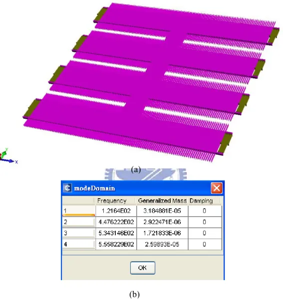
Fig. 2.17 (a) Device solid model (b) CoventorWare modal analysis...36
Fig. 2.18 SW2 closes (a) on time (b) early (c) late ...38
Fig. 2.19 Output power loss versus timing error ...39
Fig. 2.20 Layout view of the variable capacitor and switches...40
Fig. 2.21 Layout view of the previous device...41
Fig. 2.22 (a) Front side SW1 layout view in our previous design (b) modified design ...43 Fig. 2.23 (a) Overlap region between fingers and substrate (b) overlap region removal
...43
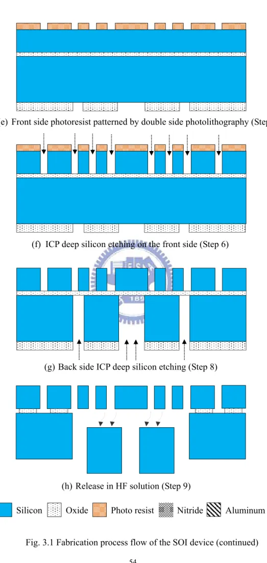
Fig. 3.1 Fabrication process flow of the SOI device...53
Fig. 3.2 Notching effect ...57
Fig. 3.3 (a) Notching occurred on the fingers bottom side, (b) improvement result ...58
Fig. 3.4 SEM photo with different C4F8 flow time (a) SF6: C4F8 = 11s:10s (b) SF6: C4F8 = 11s:7s ...59
Fig. 3.5 (a) Polymer produced in the ICP etching (b) polymer removal by NH3 solution...60
Fig. 3.6 Experiment results in the plasma permeate on the front side ...61
Fig. 3.7 Schematic of poor step coverage ...62
Fig. 3.8 Aluminum deposition by shadow mask...63
Fig. 3.9 Center hole of the fabricated device ...64
Fig. 3.10 (a) Corner of device with aluminum deposition (b) Close up view of the serpentine spring ...65
Fig. 3.11 Close-up view of finger (a) width (b) perpendicularity...65
Fig. 3.12 Device with silicon nitride coating...66
Fig. 3.13 Device with the external mass on the PCB board ...66
Fig. 4.1 (a) MMA system (b) Close view of the device on the mini-shaker (c) vibration amplitude of mini-shaker...69
Fig. 4.2 MMA experiment results with metal ball (a) amplitude response (b) phase response...70
Fig. 4.3 (a) Measurement schematic (b) our mechanical measurement setup ...72
Fig. 4.4 (a) Static device (b) device operates at resonant frequency of 116 Hz (c) resonance acceleration waveform. ...73
Fig. 4.5 Leakage resistance measurement circuit ...74
Fig. 4.6 Variable capacitor measurement circuit...75
Fig. 4.7 RC discharge time constant measurement for PECVD deposition (a) Zero displacement, time constant τ=95 μs (b) maximum displacement of 25 μm, time constant τ=287 μs...76
Fig. 4.8 Measured variable capacitor versus displacement...76
Fig. 4.9 Cross-section of non-parallel capacitor ...77
Fig. 4.10 Cactual/Cideal versus oblique angle ...78
Fig. 4.11 SEM photo (a) Close up of non-parallel capacitance (b) unflat surface of finger sidewall...78
Fig. 4.12 RC discharge time constant measurement for LPCVD deposition (a) zero displacement, time constant τ = 1.13 ms (b) maximum displacement of 25 μm, time constant τ = 4.36 ms ...79
Fig. 4.14 AC mode power measurement circuit ...81
Fig. 4.15 AC power measurement with mass attached for various load resistances (a) 2.5 MΩ (b) 3.33 MΩ (c) 10 MΩ ...82
Fig. 4.16 AC power measurement with various load resistance ...83
Fig. 4.17 Simulation results for AC model circuit ...84
Fig. 4.18 Schematic of parasitic variable capacitor Cb generation ...84
Fig. 4.19 DC model with mechanical switches...85
Fig. 4.20 Mechanical switch SW1 is (a) turning off (b) turning on...85
Fig. 4.21 Charge Voltage...85
Fig. 4.22 Voltage on the variable capacitor...86
List of Tables
Table 1.1 Comparison of power sources...8
Table 1.2 Three type of energy converter comparison...13
Table 2.1 Variable capacitor design parameters...32
Table 2.2 Spring design parameters ...35
Table 2.3 Design parameter for previous device ...42
Chapter 1 Introduction
Micro-Electro-Mechanical System (MEMS) is a technology which combines optical, mechanical, electronic, control, physical, chemical, and biomedical subsystems on a common substrate through micro fabrication processes. Application of the technology can improve the quality, performance, and reliability of the system. It can also reduce the cost due to miniaturization. MEMS have made possible the realization of the concept of system on chip (SOC). Current microsystem technology has been applied in fields such as sensors and actuators, micro optical systems, biomedical systems, aerospace and defense systems, and even entertainment applications.
Due to the advance of microsystem technology and the needs from consumers, highly integrated portable devices have received increasing interests in recent years. However, power consumption is a major problem on the development due to the limited energy capacity of the small storage devices [1]. Traditionally, energy is stored in storage devices such as batteries [2], micro-batteries [3], micro-fuel cells [4], ultra capacitors [5], micro heat engine [6], and radioactive materials [7]. High efficiency and low power loss are necessary to lengthen the life of the portable devices. Researchers have attempted to increase the energy density in these storage devices, but the solutions still have finite lifetime and high maintenance cost.
Low power CMOS VLSI (Very Large Scale Integrated circuit) technology and low duty cycles have enabled the development of such applications as wireless sensor networks or personal health monitoring. These devices have reduced power requirements in the range of tens to hundreds of microwatts [8]. It becomes possible to power these sensor nodes by scavenging ambient energy from the environment.
One can design a self-sustainable or self-renewable energy device that can replenish part or all of the consumed energy by utilizing and scavenging the energy from the environment.
1.1 Literature review
Many state-of-art technologies can scavenge or harvest energy from the environment, such as light exposure, thermal gradients, human power, air flow, acoustic noise, and vibration [9]. Energy harvesting is to convert ambient energy into electrical energy. The environment has an inexhaustible energy supply compared with the common storage devices like batteries and fuel cells. Various approaches to extract energy from the environment to drive low power electronics are studied and compared in this chapter. As a result, the performance of the energy devices is characterized by their power density, instead of energy density used for traditional storage devices.
1.1.1 Light exposure
A popular and mature method to scavenge energy is light exposure. Solar cells or photovoltaic cells are the leading technology to convert solar radiation directly to electricity with high conversion efficiency. It can provide power at low operating cost, and is virtually free of pollution. Photovoltaic cells function by the photovoltaic effect [10], the generation of voltage when a device is exposed to light. The photons of the incident solar radiation excite the electrons in the semiconductor, thus allowing the electrons to move freely and the electric current to run through the load. The operation schematic is shown in Fig. 1.1. The device has efficiencies ranging from 12% to 25% for single crystal silicon. The thin film polysilicon and amorphous silicon cost less than single crystal silicon cells but have lower efficiency [11]. Overall, photovoltaic
energy conversion offers sufficient output power besides being a mature IC-compatible technology. Nevertheless, the output power of photovoltaic devices depends heavily on the environmental conditions. For instance, the photovoltaic cells
offer adequate power density up to 15 mW/cm2 if the device is outdoors and operated
primarily during daytime. However, in normal indoor office lighting, the same
photovoltaic cell will only produce about 10 μW/cm2. Because of this characteristic,
photovoltaic cells are restricted to specific applications.
Fig. 1.1 Photovoltaic energy conversion [10]
1.1.2 Thermoelectric effect
Temperature variations can serve as a power source. This phenomenon is called the Seebeck effect, or the thermoelectric effect [12]. When two differential metals are connected in a closed loop, temperature variation in the loop causes the electron movement and a potential is built up between the two metals or semiconductors junctions.
The developed voltage is proportional to the temperature different between the hot and cold ends, and to the Seebeck coefficients of the two materials. Large Seebeck coefficients and high electrical conductivity can improve conversion efficiency and minimize power losses. Materials typically used for thermoelectric energy conversion
Photovoltaic cell Phosphorous-doped (n-type) Boron-doped (p-type) DC current flow Light exposure Electrical load
include such as Sb2Te3, Bi2Te3, Bi-Sb, PbTe, Si-Ge, polysilicon, BiSbTeSe compounds, and InSbTe, which are not completely compatible to the IC process. In [13], different annealing conditions have strong influence on the electrical resistivity of Bi-Sb and consequently the thermoelectric generator performances. An output
power density of 140 μW/cm3 for a 100 ˚C temperature gradient is obtained but the
temperature difference of this level is not common in a micro system [14]. So the output power is limited without large thermal gradients. The thermocouple element is used to produce larger output voltage, as shown in Fig. 1.2. Thus, connecting several thermocouple elements in a series configuration can be beneficial. However, large series resistance increases ohmic power loss and thus reduce the overall power conversion efficiency.
Fig. 1.2 Thermoelectric energy converter [12]
1.1.3 Human body movement
Electronic productions like PDAs or notebook are often limited by the battery capacity and necessity for recharging. Therefore, it is feasible to alleviate these problems by harvesting energy from the human movement. In recent years, needs of wearable electronic devices [15, 16] have grown significantly. Electric energy has been extracted by scavenging waste power from human activities, such as breathing,
body heat, arm motion, and walking. More attention is given to walking since this process seems a more practical source of power for the wearable electronic device.
For example, a small women’s shoe has a footprint of approximately 116 cm2, as
shown in Fig. 1.3. The shoe contains a piezoelectric shoe insert and the deformation of the piezoelectric pile generates power when walking. In addition, the motion of heels might be converted to electrical energy through traditional generator like spring. The energy stored in this compressed spring can be returned later in the gait to the user. Consequently, a maximum electrical power of 8.4 W could be generated by a 52 kg user at a brisk walking pace.
Fig. 1.3 Shoe generation system [15]
This energy could be used in a variety of low-power applications, such as pagers, health monitors, self-powered emergency receivers, and radio frequency identification tags. The application is limited by the piezoelectric and IC integration issues as well as power delivery issues. The piezoelectric shoe inserts offer a good solution for specific requirement such as RFID tags or other wireless devices worn on the foot.
Piezoelectric insert
1.1.4 Acoustic noise
Acoustic noise is usually considered as pollution but it can be seen as a power
source. In [17], the power density of acoustic noise is 0.96 μW/cm3 at 100 dB. The
energy level was lower than the power source as mentioned above. Moreover, sound volume of 100 dB closes to the airplane engine, which exceeds the tolerance of human ears. Thus, the power source from the noise is not practical. Recently research and development of this method has extracted limited power from noise with extremely high noise level. Therefore, it is not a feasible power source for common application.
1.1.5 Wind
Wind power is a renewable energy, which is the conversion of wind energy into a useful form like electricity by wind turbines or windmill. A simple eight-blade windmill that could generate electrical power from wind was developed, as shown in
Fig. 1.4(a) [18]. The windmill consists of a 750 cm2 base and a 70 cm long upright,
which are used to support the structure. On one end of the axial part there was a pulley which drives the generator, as shown in Fig. 1.4 (b). The generator was designed to working of electromagnetism. A piece of plastic pipe had plastic circles
glued to it to form a bobbin for the coil wire. Two magnets were attached on the axial
part of plastic pipe. Therefore, the magnets are held in place by their own attraction but it should be glued them in place to promise that they rotate without hitting the sides.
In this case, the power from wind is related to the air velocity. With slow wind
at 3 m/s velocity, the average power is about 80 μW /cm3. The maximum average
power density of 1060 μW /cm3 at 12 m/s air velocity was produced from a strong
Fig. 1.4 (a) Photo of the windmill, (b) close-up of the simple generator [18]
1.1.6 Ambient Vibration
Ambient vibration was present in many environments. Most sources of vibrations in the environment are at low frequencies between 60 and 200 Hz [9]. Low level mechanical vibration occurs in exterior windows, aircraft, automobile, industrial environments, and small household appliances. The maximum power is extracted at resonant with ambient vibration. Theory and experiments show that more than 300
μW/cm3 can be generated [19]. A more detailed discussion of this method is presented
in Chapter 2.
1.1.7 Summary of power sources
Comparison of the power source and energy storage devices is shown in Table 1.1. The table presents power sources and the values are estimates taken from literature or analysis. Based on the above survey, vibration is chosen as the source of energy scavenging due to its ubiquity and sufficient power density.
(a) (b) Generator Pulley Stand Blade Magnet
Table 1.1 Comparison of power sources
Power sources Power density Commercially available?
Solar (outdoors) [10] 15, 000 μW/cm2 Yes
Solar (indoors) [10] 10 μW/cm2 Yes
Temperature gradient [13] 140 μW/cm3 at 100˚C gradient Soon
Human power [15, 16] 330 μW/cm2 No
Acoustic noise [17] 0.96 μW/cm3 at 100dB No
Wind energy [18] 1060 μW/cm3 at 12 m/s velocity No
Vibration [19] More than 300μW/cm3 No
1.2 Ambient vibration energy conversion
According to the previous overview, ambient vibration can be used to convert energy into electrical power which is discussed in this section. Three methods are typically used to convert vibration energy to electrical power. There are respectively piezoelectric conversion, electromagnetic inductive conversion, and the electrostatic capacitive conversion.
1.2.1 Piezoelectric energy conversion
The piezoelectric energy conversion converts mechanical energy to electrical energy by the piezoelectric effect of a piezoelectric material. The piezoelectric energy converters are based on two-layer benders (or bimorphs) mounted as a cantilever beam with a mass attached, as shown in Fig. 1.5 [19]. The top and bottom layers of the devices are composed of piezoelectric materials. When the beam bent down, it produced a tension in the top layer and compresses the bottom layer. A voltage is built across each of the layer which we can condition and use to drive a load circuit.
Energy harvesting circuitry for piezoelectric were already reported in [20]. The objective of this paper is to develop an approach that maximizes the power transferred from a vibrating piezoelectric transducer to an electrochemical battery. Due to the AC signal produced by the piezoelectric element and the needs of DC voltage for the circuit, an AC-DC rectifier must be connected to the output of the piezoelectric device. In this circuit, the maximum output power was 18 mW with a power density of 1.86
mW/cm3 for the vibration frequency of 53.8 Hz.
Other works on piezoelectric converters were also conducted [21], which utilized the piezoelectric film of PZT deposited on a steel cantilever by a low temperature process. But this material is not compatible with the IC process. Another drawback of piezoelectric converter is the requirement of the additional circuitry to rectify the AC current and convert the extracted power. The supplementary circuitry has power losses and decreases the efficiency of the conversion. Most researches so far utilize bulk materials, which is not suitable for integration with microsystem technology.
Fig. 1.5 A two-layer cantilever beam piezoelectric energy converter [19]
1.2.2 Electromagnetic energy conversion
In electromagnetic energy conversion, any magnetic flux linkage changes in a coil can induce a voltage or electromotive force (EMF) from Faraday’s law. A typical electromagnetic energy converter is shown in Fig. 1.6 [22]. Mechanical acceleration is
produced by vibrations that cause the mass to move and oscillate. A coil is attached to the mass and moves through a magnetic field built by a permanent magnet. The induced voltage was produced by the change of magnetic flux. Thus, the output power is proportional to the magnetic field and coil number.
Fig. 1.6 Electromagnetic energy converter [22]
Cao [23] has presented a novel integrated electromagnetic generator system which has a maximum output power level of 35 mW for the vibration source with an amplitude of 3 mm and frequency of 40 Hz. The system consists of an electromagnetic power generator, an interface electronic circuit and an energy storage device, as shown in Fig. 1.7. The energy harvesting circuit was implemented on a 0.35-μm CMOS IC chip.
The most common issue for electromagnetic energy conversion is the relatively low induced voltage. Methods to increase induced voltage include increasing the number of turns of the coil or increasing the permanent magnetic field. However, it is difficult to fabricate large number of coils with planer thin film processes. Thus the power density of electromagnet converter is lower than other types of device.
Fig. 1.7 Schematic of an electromagnetic generator system [23]
1.2.3 Electrostatic energy conversion
Electrostatic capacitive energy conversion depends primarily on the changing capacitance of a variable capacitor, as shown in Fig. 1.8.
Fig. 1.8 (a) Gap-closing and (b) overlap in-plane variable capacitors [22]
The variable capacitor is pre-charged initially and subsequently disconnected from the source. In the constant charge Q process, the capacitance decreases due to vibration between the fingers. Now the voltage on the variable capacitor increases (Qconstant=CV) and thus converts the kinetic energy into electrical energy.
The feature of the electrostatic energy converter is its IC process compatibility. MEMS variable capacitor can be fabricated through mature silicon-based micromachining process such as deep reactive ion etching. Therefore, it is suitable for conventional IC process. The converter also provides high output voltage levels and adequate power density. However, the disadvantage of the converter is the need of an
auxiliary voltage source Vin to initiate the conversion cycle. Therefore, the lifetime of
the voltage source is limited. The issue can be solved by employing inductive flyback circuitry proposed by Bernard et al. [24], which constantly feedbacks the temporary storage energy to the external voltage supply for further usage. Besides, one can also employ a moving layer of permanently embedded charge, or electret, to carry out electric energy harvesting [25], although such systems currently have power densities inferior to those using variable capacitors.
A capacitive energy converter was implemented by Meninger et al. [26]. The comb finger structure was used in MEMS technology with silicon on insulator (SOI) wafers. The simulation showed an output power of 8.6 μW with a device size of 1.5 cm × 0.5 cm× 1 mm from the vibration source of 2.52 kHz. Another design was proposed by Roundy [9], which could achieve an output power density of 110
μW/cm3 under vibration input 2.25 m/s2 and frequency of 120 Hz.
In capacitive energy conversion, the switch timing control should be controlled accurately in order to optimize conversion efficiency. A prototype circuitry with the two ideal diodes was proposed by Roundy [9]. The experimental results showed excessive power reduction due to the far from ideal operation of the diodes. The power consumption by the electronics or parasitic capacitive and resistive coupling still existed in the designs. Therefore, improved switch design is critical for better energy conversion efficiency.
1.2.4 Comparison of energy conversion technologies
According to the above literature overview, the three types of energy converter are listed in Table 1.2 [22]. According to the characteristic comparison of these energy converters, electrostatic capacitive vibration-to-electric energy conversion is suitable for scavenging ambient energy because of ubiquity in the environment and sufficient output power density. The fabrication technologies for electrostatic converter are very mature in MEMS system. The materials and process are compatible with IC process.
Table 1.2 Three type of energy converter comparison [22]
Type Estimated power (in 1 cm2 or 1 cm3)
Piezoelectric ~200 μW
Electromagnetic < 1μW
Electrostatic 1-100μW
1.2.5 Our previous work
Our past design of capacitive energy conversion with integrated mechanical switch has been conducted [27]. The achievement of the previous device includes the realization of integrated mechanical switches. Besides, the improvement of fabrication process and electrical power measurement was conducted. However, the leakage resistance was existed in the variable capacitance.
1.3 Thesis objectives and organization
Our previous design [27] shows the mechanical switches can be integrated successfully in the electrostatic generator in order to acquire the precise timing control. Besides, the parasitic effect causes power dissipation due to fabrication errors. More
detail will be presented in Chapter 3. Therefore, the goals of this thesis are as the following:
(a) Design and analyze of the optimal power for the electrostatic converter with no external mass attached,
(b) Propose novel theory for describing the dynamic model of energy converter, (c) Improve the performance and eliminate unwanted parasitic effects,
(d) Continue the AC mode circuit measurement with external mass and DC mode circuit test on the devices.
The organization of this thesis is as the following. The principle and design of the energy converter are presented in Chapter 2. The fabrication process and results are described in Chapter 3. The measurement results and discussion are shown in Chapter 4. Finally, conclusion and future work are discussion in Chapter 5.
Chapter 2 Principle and Design
Micro electrostatic capacitive energy converter relies on the change of capacitance of a variable capacitor caused by vibration. Thus, the kinetic energy is converted into the electrical energy during this process. The variable capacitor is initially charged by an external power supply such as a battery. The charge-discharge cycles are controlled by switches. The optimum design and analysis will be presented in this chapter. Theoretical model was established to describe the device characteristics and also compared with simulation model of our previous design.
2.1 Characteristics of vibration sources
As mentioned above, vibration sources are generally more ubiquitous. The output power of a vibration driven converter depends on the nature of the vibration source, which should be known in order to estimate the generated power. There are various kinds of vibration sources in the environment. Measurement of different vibration sources was conducted by Roundy [9], as shown in Fig. 2.1. From the low level vibration sources, two results can be observed. First, fundamental peaks occur at a common low frequency. Second, the high frequency vibration modes are lower in acceleration magnitude than the low frequency fundamental modes. Low level vibration in typical households, offices, and manufacturing environments is considered also as a possible power source for wireless sensor nodes.
Our measurement of the vibration spectrum of a dehumidifier is shown in Fig. 2.2. A piezoelectric accelerometer was put on the dehumidifier and the data was collected by an oscilloscope. The fundamental vibration mode is at about 120 Hz, as
about 120 Hz, as shown in Fig. 2.3. These results will be used as our targeted input vibration source due to its common existence.
Fig. 2.1 Vibration spectra by Roundy [9]
Fig. 2.2 Measurement of dehumidifier vibration Dehumidifier
To oscilloscope Accelerometer
Fig. 2.3 Vibration spectrum of a dehumidifier
2.2 Operational principle
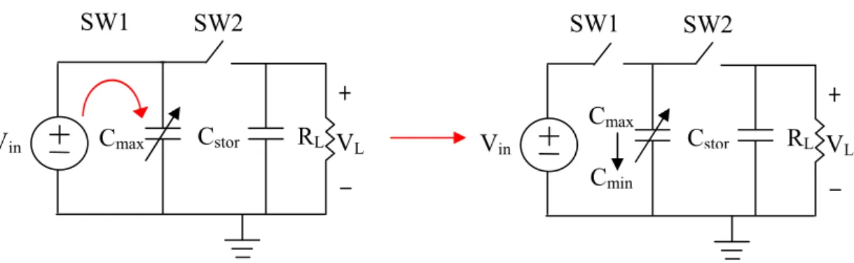
The main component of the electrostatic energy converter is a variable capacitor
Cv [28]. A schematic circuit of the energy converter is shown in Fig. 2.4. It is
composed of an auxiliary battery supply Vin, a vibration driven variable capacitor Cv
and an output storage capacitor Cstor, which is connected to the load RL. Two switches,
SW1 and SW2, are used to connect these components and control the charge-discharge conversion timing [27].
Fig. 2.4 Operation circuit of the electrostatic energy converter
A B C D Vin Cv Cstor RL VL SW1 SW2 20 70 120 170 220 Frequency (Hz) 1 10 0.1 Acceleration ( m/s 2 ) 0.01 0.001 100 2.2 m/s2at 120 Hz
A more detailed schematic of the energy converter is shown in Fig. 2.5. The change of the capacitance is driven by the external vibration source. SW1 is implemented by a contact mechanism between nodes A and B. SW2 is actuated the electrostatic pull-in force between nodes B and D. When the node B reaches the pull-in voltage, it will be attracted by the node D and touch node C.
Fig. 2.5 Variable capacitor schematic
In the beginning, the variable capacitor Cv is charged by the auxiliary voltage
supply Vin through the switch SW1 when Cv is at its maximum Cmax, as shown in Fig.
2.6. After Cv is charged to Vin, SW1 is opened and the capacitance changes from Cmax
to Cmin due to the electrode displacement by vibration. In the process, the charge Q on
the capacitor remains constant (SW1 and SW2 both open). Therefore, the terminal
voltage across the capacitor Cv is increased and the mechanical energy is converted to
the electrical energy stored in the capacitor.
Fig. 2.6 Capacitor charging and capacitance change by vibration
VL Cmax Cstor Vin SW2 RL SW1 VL Cmax Cstor Vin SW2 RL SW1 Cmin SW1 A B Displacement C D
SW2 Cstor Pull-in electrode
RL
Cmin Cstor RL VL SW2 VL(t) SW2 open (Discharging) SW2 close (Charging) ‧‧‧ Vsat ‧‧‧ V0 VL[n, t=tn] VL[n-1, t=tn-1+Δt] tn tn-1 Δt
When the capacitance reaches Cmin and terminal voltage reaches Vmax, SW2 is
closed and the charge redistributes between Cv and Cstor, as shown in Fig. 2.7 [29].
The energy stored in the variable capacitor Cv is transferred to the the storage
capacitor Cstor. SW2 is then opened and Cv varies back to Cmax, preparing for the next
conversion cycle. The charge on Cstor is dissapated through the load resistance RL with
a time constant τ = RLCstor before it is charged again by Cv. The output voltage VL
will eventually reach the steady state when the initial and final voltages of the charge-discharge process become equal.
Fig. 2.7 Charge transfer and discharge process [29]
Let the conversion cycle time be Δt, the output voltage of the n-th cycle before and after the charge transfer can be expressed as [29]
L n-1 stor max min L n stor min [n-1, + ] + [n, ] = , + = Δ = V t t t C V C V t t C C (2.1)
where Vmax is equal to VinCmax/Cmin, VL [n-1, t = tn-1+Δt] is the voltage before the
charge transfer, and VL [n, t = tn] is the voltage after the charge transfer. After SW2 is
opened, the output voltage in this charge dissiaption period can be expressed as
L n stor max min
L n L stor stor min [n-1, = t + ] + [n, = + ] exp(- / ), + Δ Δ =V t t C V C × Δ V t t t t R C C C (2.2)
If the charge transferred to Cstor is more than that discharged through the output load,
the net increment will result in the rises of VL step by step. In the steady state, the net
becomes the same. From the Eq. 2.2, the final saturation voltage of the output terminal can be derived as
max in stor sat min L stor stor = , (1+ ) exp( t/× Δ )-1 C V C V C R C C (2.3)
where Δt = conversion cycle time = 1/2f and f is the vibration frequency. The average output power can be calculated as
L stor - / 2 2 0 L L L (V e ) (t) (t)= = , t R C V P R R (2.4) 2 2 Δt stor 0 sat out 0 L stor L 1 -2Δt = P(t)dt= [1-exp( )] , Δt
∫
2Δt R C ≈ R C V V P (2.5) where / L s to r 0 s a t Δ = × t R CV V e , as shown in Fig. 2.7. The approximation takes place
when Δt << RLCstor, which also results in a small output voltage ripple.
2.3 Device design
The main design and analysis are about the variable capacitor structure. In our previous designs [29], an external mass should be put on the center hole of the electrostatic converter to adjust the resonant frequency to 120 Hz as mentioned above. The mass of the microstructure below the external mass was ignored. Therefore, the focus of the design is on the optimum power analysis of the device with no external mass attachment. Due to the small mass of microstructures, a little vibration force is needed to drive the variable capacitor structure. Another advantage is to increase the power density because of decreased volume of the device. In the design without the external mass, the vertical force during the vibration is reduced so that the microstructure damage can be alleviated.
The optimum power analysis is based on Eq. 2.5. The power strongly depends on
indicating that it influences the device vibration movement. Due to the constraint of 1
cm2 device area and electrostatic force, the maximum capacitance was limited and
thus influencing the subsequent variable capacitor design.
2.3.1 Auxiliary power supply
The auxiliary power supply is used to pre-charge the variable capacitor through SW1. The power supply can be a capacitor or rechargeable battery. But this power supply has lifetime and mass issues in some microstructure. In [24], the researcher provided a good method to store the converted energy to convert energy in storage elements in order to provide power and energy more smoothly. In the device without the external mass, the input voltage was chosen as 0.3 V of solar battery to reduce the electrostatic force and avoid the pull-in phenomenon in the charging process.
2.3.2 Static analysis
The static analysis is conducted to obtain mathematical guidelines for deciding
overall parameters. With Eq. 2.3 the circuit components can be chosen such that Cstor
>> Cmin and RLCmin << Δt. Therefore, Eq. 2.3 can be simplified as
max in max in sat L min L min C V C V V = R . t t C R C ≈ Δ Δ (2.6)
The output power becomes
2 2 sat max in out L L V C V P R . R t ⎛ ⎞ ≈ ≈ ⎜ ⎟ Δ ⎝ ⎠ (2.7)
From the Eq. 2.5, it is possible to find the optimal power obtainable by first
0, out L dP dR = , max 1 2 ln 1 L opt stor stor R C fC C = ⎛ ⎞ + ⎜ ⎟ ⎝ ⎠ (2.8)
The optimal load resistance depends on the storage capacitor Cstor and the maximum
capacitance Cmax. The constraint on Cmax was discussed as mentioned above. With the
Eq. 2.6, the output voltage is below 16 V for the further power management circuit.
Thus, the minimum optimum load resistance is 50 MΩ. Cstor was chosen to be 5 nF
for an output voltage ripple lower than 1 V, which has no effect on the output power from Eq. 2.7.
2.3.3 Dynamic analysis
The objective of dynamic analysis is to determine the relationship between the mechanical spring force and the electrostatic force to achieve the desired maximum displacement under the targeted input vibration. The electro-mechanical dynamics of the variable capacitor can be modeled as a spring-damper-mass system, as shown in Fig. 2.8
Fig. 2.8 Schematic of the conversion dynamic model
Fixed plate m k bm k be k z(t) y(t) Movable plate
The dynamic equation is
.. . ..
e m
m z + b z+ b (z) + kz = -m , z y (2.9)
where y is the displacement of device frame caused by the vibration, z is the relative
displacement between movable and fixed plate, k is spring coefficient, b (z) zm . is the
mechanical damping force caused by the squeeze film effect, and b z is the e
electrostatic force caused by the charge on the capacitor, which acts as a negative
spring force with be as the electrostatic spring constant.
In Eq. 2.9, bm(z) is a function of z. Therefore the system is nonlinear. In order to
simplify the analysis, we assume the system is operated in the low damping environment and squeeze film effect is ignored. Constant damping is used as an approximation. The vibration source is assumed to be sinusoidal with complex amplitude Y and frequency ω, and the relative displacement with complex amplitude
Z, Fourier transform is applied to solve the equation
2 2 2 2 2 e m = . ( + - ) + m Z Y k b m b
ω
ω
ω
(2.10)The equation shows the equivalent spring constant is '
e
k = +k b . The electrostatic
spring coefficient influences the spring coefficient. Thus, the resonant frequency of system is e n 2 e g 2 k b m Q b N Ad
ω
ε
+ = = (2.11)where Q is charge on the variable capacitor, Ng is number of comb cells, A is overlap
area and d is initial gap between the fingers. These parameters are discussed in detail in the next section. In order to maintain steady resonance, the mechanical spring
constant k should be relatively larger than the maximum electrostatic spring constant (be_max). The relationship between the spring k and be_max was already discussed in
[27], which presented the ratio of these two parameters rd increased with the desired
maximum displacement zmax by Simulink model. But the phenomenon described by
Simulink model has no explicit theoretical foundation. Therefore, the detailed description is considered by using theoretical analysis. From the Eq. 2.11, the
electrostatic spring coefficient be is determined from the charge Q and thus this is a
square wave function, as shown in Fig. 2.9.
Fig. 2.9 Electrostatic spring constant in the steady state
From the Eq. 2.9 and Eq. 2.11, the vibration source is assume the sinusoidal wave
(y=Y0sinωt). In order to solve the equation theoretically, the relative displacement can
be described by the two government equations.
a a a 0 0 0 a e_max b b b 0 0 0 b e_min sin , sin , m a m b b k z z z Y t k k b m m b k z z z Y t k k b m m ω ω ω ω 2 2 + + = = + + + = = + gg g gg g (2.12)
where za is relative displacement between fingers before discharging, zb is relative
displacement after discharging, as shown in Fig. 2.9. The damping coefficient bm was
0.97 0.975 0.98 0.985 0.99 0.995 1 -5 0 5x 10 -5 Time(s) M ova bl e f inge rs di sp la ce m en t( um ) 0.97 0.975 0.98 0.985 0.99 0.995 10 5 10 be be_max be_min Charge Discharge Time (s) be za zb
Movable fingers displacement (
μm) 50
assumed to be constant in the low damping environment. Thus, the equations are linear so that solutions are as follows
(
)
1 a a 1cos da 2sin da pa( ) t z =e−ζ ω Cω
t+Cω
t +z t (2.13a)(
)
2 b b 3 db 4 db pb z t cos sin ( ) e−ζ ω Cω
t Cω
t z t = + + (2.13b) where 2 2 a b m m a b a da a a b db b b a b ; 1 , , 1 . 2 2 k k b b m m m m ζ ζ ω ω ω ζ ω ω ω ζ ω ω = = = , = − = = −zpa and zpb are the particular solutions of the equation. The two equations can be
solved numerically to get a suitable solution. As mentioned above, be_max must be
smaller than spring constant k. Therefore, the coefficient ka (ka=k+be_max) was
considered. From the Eq. 2.13(a) and Eq. 2.13(b), the desired displacement (z=za+zb)
is relative to the electrostatic spring constant (be_max and be_min). The desired
maximum displacement was decreased progressively with the maximum electrostatic spring constant be_max raising. We can utilize the relationship to determine the desired
maximum displacement zmax by using various maximum electrostatic springs constant.
The theoretical analysis results can be compared with the simulation from Simulink, as shown in Fig. 2.10. It shows that the maximum electrostatic spring constant be_max
should be smaller than the mechanical spring constant k to maintain the steady resonance. Thus, the minimum ratio of k/be_max can be determined from the desired
maximum displacement. From the Fig.2.10, the maximum displacement zmax was
approximately proportional to the minimum ratio of k/be_max (rd) for the theoretical
value, which can be written as following equation:
d 0.0875 max 0.8
r ≈ z + (2.14) It can be viewed as a linear function.
Fig. 2.10 k/be_max versus the desired maximum displacement
2.3.4 Variable capacitor design
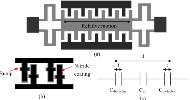
From [29], the in-plane gap closing comb structure is used for the variable capacitor, as shown in Fig. 2.11. In Fig. 2.11(a), the dark areas are anchor regions and the light areas are movable regions. The spring of the in-plane gap closing variable capacitor makes it easier to move perpendicular to the finger gaps. Fig.2.11 (b) shows the comb fingers with silicon nitride deposited on the sidewalls for electrical insulation.
Fig. 2.11(a) Top view of the in-plane gap closing variable capacitor, (b) fingers with silicon nitride coating, (c) equivalent capacitance model between fingers
Cdielectric Cdielectric Cair d t t (c) (b) Nitride coating Bump (a) Relative motion 20 25 30 35 40 45 50 55 60 65 70 2 3 4 5 6 7 maximum displacement(um) k/b e m ax Theoretical value simulation value rd~0.0875zmax+0.8
Desired maximum displacement (μm)
k/b
The symbols used in the following analysis are listed below d : initial gap between comb fingers,
t : thickness of silicon nitride coated on the sidewalls of fingers, Lf : overlap length of comb fingers,
Wf : comb finger width,
h : thickness of comb fingers,
Ng : number of variable capacitor cells,
z : relative displacement between the movable and fixed electrodes, ε0 : permittivity of free space,
εr : relative permittivity of silicon nitride (εr=7)
The thickness of silicon nitride t is 500 Å to avoid the electronic tunneling effect in the charging process. The bumps on the sidewalls of the fingers keep the minimum finger spacing at 0.5 μm. Fig. 2.11 (c) shows the equivalent air gap of the capacitor is eq
r
2t d = d - 2t +
ε
with dielectric thickness t and relatively permittivity εr. The total
variable capacitance between the comb fingers is [29]
r v g o f 2 2 r 2t 2( +d-2t) ε C (z)=N ε L h . 2t ( +d-2t) -z ε ⎛ ⎞ ⎜ ⎟ ⎜ ⎟ ⎜ ⎟ ⎜ ⎟ ⎝ ⎠ (2.15)
From this equation, the variable capacitance strongly depends on the comb finger structure. A general model of the comb finger structure is shown in Fig. 2.12. The layout includes the movable plate and fingers. A number of free parameters can be adjusted to obtain the optimal output power. The guideline of the optimization of parameters was also presented in [30, 31].
As mentioned above, the output power of the device is produced by the variable capacitor, which is formed by the comb fingers. W0 and L0 are the width and length of
Lf d L0 W1 W1 W2 W0 z x y Fingers Movable plate
the layout. W1 is the movable plate width on both side in the x-axis direction and W2
is in the y-axis direction. These two parameters determine the mass of the movable plate. W1 should be designed as large as possible because it determines the number of
fingers, which is related to the output power. But the initial gap between fingers d also influences the number of fingers for a given chip area constraint. W2 is determined by
the overlap length of fingers Lf. In order to have much output power, the comb
structure center width should be designed as small as possible to have much number of fingers. But the robustness should be considered during vibration. Without external mass attachment structure design, the comb fingers structure has the center width of 1000 μm to ensure the robust structure and power requirement.
Fig. 2.12 A general model of the movable plate
The output power versus variable capacitor parameters is calculated according to Eq. 2.5 and Eq. 2.6. Device will be fabricated on the SOI wafer. The thickness h is choosing as 200 μm to have large capacitance. The finger width Wf of 10 μm is
restricted by the aspect ratio up of to 20:1 in the deep reactive ion etching process. The mechanical damping force between fingers for large displacement is [32]
3 3 . . . g f g f m m 1.5 3 3 2 μN L h μN L h F =b (z) z = α z α z, (d-2t) z (d-2t) 1-( ) d-2t ⎛ ⎞ ⎜ ⎟ ⎛ ⎞ ⎜ ⎟ ≈ ⎜ ⎟ ⎜ ⎟ ⎜ ⎡ ⎤ ⎟ ⎝ ⎠ ⎜ ⎢ ⎥ ⎟ ⎣ ⎦ ⎝ ⎠ (2.16)
with b (z) as the equivalent mechanical damping constant. Device was operated in m low damping environment that can improve the quality factor especially. The squeeze film damping effect can be ignored in the low damping environment. Thus, the mechanical damping constant is independent of the relative displacement z. Thus, the damping force is proportional to the velocity z . The electrostatic force induced by . the charge Q on Cv is [28] 2 e e g o f r -Q F =b z= z. 2t 2N ε L h( +d-2t) ε ⎡ ⎤ ⎢ ⎥ ⎢ ⎥ ⎢ ⎥ ⎢ ⎥ ⎣ ⎦ (2.17)
The force is proportional to the negative displacement of the movable plate. The be
can be regarded as the electrostatic spring constant. The electrostatic spring constant is determined by the charge Q on the variable capacitor which varies in the charge-discharge process. The maximum electrostatic spring constant be_max will
reduce the total spring constant and make the movement unsteady during the vibration. Therefore, the be_max should be limited as
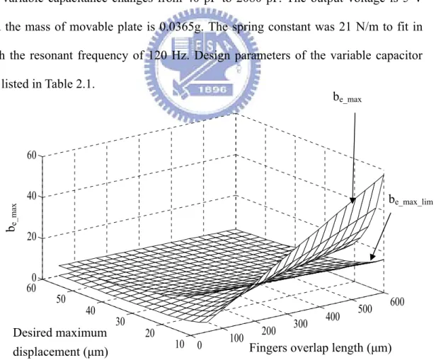
2 2 max n e_max e_max_lim d d g o f r = , 2 2 ( + -2 ) ε Q k m b b t r r N L h d t ω ε = ≤ = (2.18) g f f 1 2 0 1 0 [2 ( ) 8 ( 2 ) ]. m=ρh N W L +d + W W + L − W W (2.19) The mass m of the movable plate is related to the density and thickness h of the device. According to Eq. 2.18 and Fig. 2.10, the limitation of the electrostatic spring constant be_max_lim is related to the ratio rd between the mechanical spring k and be_max
which increased with the desired maximum displacement (Eq. 2.14). With the above design parameters, the relationships of the be_max and be_max_lim are the functions of the
initial gap d and the finger overlap length Lf, as shown in Fig. 2.13(a). If the be_max
layer is below the be_max_lim layer, it indicated the electrostatic spring softening effect
can be ignored for the steady resonance at mentioned above. Fig. 2.13(b) is the two-dimension diagram of Fig. 2.13(a), which shows the available region that indicated be_max layer was below be_max_lim layer. Otherwise it is unavailable region. In
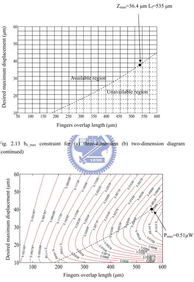
Fig. 2.14, we can obtain the maximum power of 0.51 μW (power density of 12 μW /cm3) with the maximum displacement 36.4 μm and finger overlap length 535 μm in the available region. In this analysis, the initial gap between the fingers is 37 μm and the variable capacitance changes from 40 pF to 2080 pF. The output voltage is 5 V and the mass of movable plate is 0.0365g. The spring constant was 21 N/m to fit in with the resonant frequency of 120 Hz. Design parameters of the variable capacitor are listed in Table 2.1.
Fig. 2.13 be_max constraint for (a) three-dimension (b) two-dimension diagram
0 100 200 300 400 500 600 10 20 30 40 50 600 20 40 60 be_max be_max_lim
Fingers overlap length (μm) Desired maximum
displacement (μm)
Fig. 2.13 be_max constraint for (a) three-dimension (b) two-dimension diagram
(continued)
Fig. 2.14 Output power versus desired maximum displacement and finger overlap length 0.03 248 7 0.03 248 7 0.06 078 7 0.06 078 7 0.089 088 0.08 9088 0.08 9088 0. 117 39 0.11 739 0.11 739 0.1 45 69 0.14 569 0.14 569 0.17 3 99 0.17 399 0.17 399 0.20 229 0.20 229 0.20229 0.23 059 0.23 059 0.2 3059 0.23059 0.25 889 0.25 889 0.25889 0.25889 0.28 719 0.28 719 0.28719 0.28719 0.31 549 0.31 549 0.31549 0.31549 0.34 379 0.34 379 0.3 4379 0.34379 0.37 209 0.37 209 0.37209 0.40 039 0.40 039 0.40039 0.42 869 0.42 869 0.42869 0.45 699 0.45 699 0.45699 0.48 529 0.4 85 29 0.51 359 0.51359 0.54 1 89 0. 570 19
fingers overlap length
de
si
re
d m
axi
m
um
d
is
pl
ac
em
en
t(
um
)
100
200
300
400
500
600
10
20
30
40
50
60
Desired max imum d is placemen t ( μm )Fingers overlap length (μm)
Pmax=0.51μW 50 100 150 200 250 300 350 400 450 500 550 600 10 20 30 40 50 60
fingers overlap length(um)
in iti al ga p be tw ee n fi ng er Available region Unavailable region
Fingers overlap length (μm)
Desired max imum d isplacemen t ( μm) Zmax=36.4 μm Lf=535 μm
Table 2.1 Variable capacitor design parameters
Variable Description of variables Designed value
h Device thickness 200 μm Ng Number of variable capacitor cells 788
Wf Finger width 10 μm
Lf Finger overlap length 535 μm
d Finger initial gap 37 μm
Zmax Maximum displacement 36.4 μm
t Silicon nitride sidewall thickness 500 Å Cmax Maximum value of capacitance 2080 pF
Cmin Minimum value of capacitance 40 pF
k Mechanical spring const. 21 μN/μm m Mass of movable plate 36.5mg RL Driven load resistance 50 MΩ
Cstor Output temporary storage capacitor 5 nF
Vout Output voltage (steady state) 5 V
Pout Output power (steady state) 0.51 μW
2.3.5 Spring design
In the mechanical spring design, the device without external mass attached will need a soft spring to fit in with the resonant frequency due to the small mass of the movable plate. Thus, the serpentine spring structure was considered. The primary deformation is along the direction of relative displacement so that the spring constant in the x-direction is used for device design. The schematic of folded serpentine spring structures is shown in Fig. 2.15.
Fig. 2.15 A single element of spring structure
From the schematic of spring, two beams are connected by a truss between the serpentine springs. If the truss is assumed rigid, the spring constants analysis in different direction can be expressed as [33],
= 3 x 3 4 25 NEW h k L (2.20) = y 7 NEWh k L (2.21) = 3 z 3 4 25 NEWh k L (2.22)
where N is the number of springs in the layout, h is the thickness of springs. E is the Young’s modulus of single crystal silicon, Lk and Wk are the length and width of the
beams, Lt and Wt are the length and width of the truss.
For a more extensive analysis of folded beam, including the effect of compliant trusses, the spring constant above must be multiplied by a coefficient λ [34]
2 3 6 2 3 6
a +16as +44s
λ= ,
4a +34as +44s (2.23)
Anchor Anchor Movable plate
Spring z x y Wt Lk Wk Truss Beam Lt
where a is the truss length to beam length ratio (Lt/Lk) and s is the truss width to beam
width ratio (Wt/Wk). In our design, Lt=57μm, Lk=1272μm, Wt=40μm, Wk=11μm. The
calculated λ is equal to 0.999, which implies that the effect of non-rigid trusses is small. Several issues should be considered. First, the z-axis stiffness kz and y-axis ky
should be relatively larger than the lateral x-axis stiffness kx to reduce the out-of-axis
motion. The stress in the spring should be smaller than the yield stress of single crystal silicon (7GPa). A safety factor Sf defined as the yield stress divided by the maximum stress on each axis is used to check the spring robustness. The maximum stress due to the lateral maximum displacement xmax and static vertical weight loading
are given k max x 2 k 12EW x σ = , 25L (2.24) k z 2 k 12mgL σ = , NW h (2.25) As mentioned above, the mass of the movable plate was 36.5 mg, and eight serpentine springs are connected to the movable plate. The total spring constant in the x-direction kx is 21 N/m, which is far below the other two spring constant (ky=3.04×10⁵ N/m,
kz=8408 N/m). CoventorWare finite element method simulation of a single spring
element is shown in Fig. 2.16, which has a spring constant of 2.64 N/m. The results were identical to the design value. The maximum lateral stress is when the maximum displacement is 36.4 μm. The vertical stress is 1.55 MPa, which is so smaller due to the external mass removal on the movable plate. The final devices parameters of the springs are listed in Table 2.2.
Fig. 2.16 (a) A single spring element (b) single spring constant simulated by CoventorWare
Table 2.2 Spring design parameters
Variable Description of variables Designed value
Wk Spring Width 11 μm
Lk Spring Length 1272 μm
kz Vertical spring constant 8408 μN/μm
kx X-axis spring constant 21 μN/μm
ky Y-axis spring constant 3.04×10⁵μN/μm
kz / kx Vertical stiffness ratio 401
ky / kx Lateral stiffness ratio 1.44×10⁴
Sf_x Lateral safety factor 348.69 Sf_z Vertical safety factor 4512.8
CoventorWare modal simulation of the device is shown in Fig. 2.17. The first mode is the lateral mode in the x-direction (mode 1), which is the primary mode and the frequency of 122 Hz, which is resonant frequency of device. The simulation
(b) (a)
-40
-20
0
20
40
-100
-50
0
50
100
spring displacement
sp
ri
ng
fo
rce
Spring displacement (μm) Spring force ( μN)Single spring constant kx ~2.64 N/m
results agree well with the design value. Other mode frequencies are the torsion mode (mode 2), lateral mode in y-direction (mode 3), and vertical mode (mode 4), which are at least 3.5 times higher than the primary mode. The separation is large enough to avoid stimulation of these unwanted modes by the input vibration.
Fig. 2.17 (a) Device solid model (b) CoventorWare modal analysis
2.3.6 Mechanical switch control analysis
The mechanical switches SW1 and SW2 are shown in Fig. 2.3 and Fig.2.4. Traditionally, the switches utilize diodes or clocked active switches [35, 36]. But charge leakage and reverse current issues exists in this circuit. A reverse current should be lower than a few nA in order to prevent charge leakage. However, this is not
(a)
common in commercially available diodes and other switching circuitry. Mechanical switches are utilized due to the barely zero charge leakage and lower power consumption. Other advantages are the synchronous operation to the variable capacitor and the monolithic integration with the device structure.
The detail of mechanical switch design was already presented in [27]. This section will discuss the power loss issue during the mechanical switches control process. SW1 is a contact mechanism switch. The variable capacitor charging is realized by SW1 turning on when the comb fingers of the variable capacitor touch. Mechanical switch SW2 is controlled by the pull-in voltage. When the voltage on the capacitor reaches the pull-in voltage, the node B will move to touch node C by electrostatic force, as shown in Fig. 2.5. The pull-in voltage can be determined by the following equation 3 s2 0 PI SW2 k d 2 2 V , 3 3 hL = ε (2.26) where ks2 is the SW2 spring constant, do is the initial gap between nodes B and D
(Fig.2.5), and L is the total overlap length of nodes B and C. The thickness h is the same as the variable capacitor. A number of parameters influence the pull-in voltage. Shown in Fig. 2.18 (a) is the time response of voltage on the variable capacitor and movable fingers displacement. The figure shows the SW2 turn on precisely when the fingers move to the middle position. The output power will fit in with the theoretical value as mentioned above if the device has no leakage current issue. The maximum voltage Vmax on the variable capacitor is 14 V, which is related to the ratio of
maximum and minimum capacitance,
max max in min C V V . C = (2.27) The pull-in effect occurs at one-third of initial gap between the node B and C. Fig.
2.18 (b) has the low pull-in voltage. It shows that the SW2 closes before the fingers moving to the middle position, which is caused by the soften spring constant of SW2. The voltage on the variable capacitor was lower extremely than Vmax when SW2
closes. It indicates the incomplete energy conversion and means the output power loss. Shown in Fig. 2.18 (c), the voltage on the variable capacitor reaches Vmax but the
SW2 turn on lately. It indicates that the fingers are pulled by a larger restoring force of hard spring. From the simulation result, we can find the relationship between the timing error and power loss, as shown in Fig. 2.19.
Fig. 2.18 SW2 closes (a) on time (b) early (c) late (a) 0.98 0.982 0.984 0.986 0.988 0.99 0.992 0.994 0.996 0.998 1 -5 0 5x 10 -5 time(s) fi ng er di sp la ce m ent (um ) 0.98 0.982 0.984 0.986 0.988 0.99 0.992 0.994 0.996 0.998 10 5 10 15 V ol ta ge on va ri ab le c apa ci to r( V ) Fingers middle SW2 on -50 Volta ge on v ariab le ca pa cito r Finger disp lacemen t ( μm) Time(s) 50 (b) 0.98 0.982 0.984 0.986 0.988 0.99 0.992 0.994 0.996 0.998 1 -4 0 4x 10 -5 fi nge rs di sp lacem ent (um ) 0.98 0.982 0.984 0.986 0.988 0.99 0.992 0.994 0.996 0.998 10 5 10 15 Time(s) vol ta ge on va ri abl e c apaci to r( V ) Fingers middle position SW2 turn on -40 Finger disp lacemen t ( μm) V oltage on v ariab le cap ac ito r (V) 40 Time(s)
Fig. 2.18 SW2 close (a) on time (b) early (c) late (continued)
Fig. 2.19 Output power loss versus timing error
2.4 Layout design
The layout of the movable plate was discussed in the last section. This whole schematic was designed with a symmetric configuration to maintain the mass balance and ensure the stable movement in the x-direction during vibration. The minimum center width of movable plate should be larger than 1000 μm to maintain a high rigidness. With the external mass removed, more space in the center was to design the
-2.50 -2 -1.5 -1 -0.5 0 0.5 1 20 40 60 80 100
timing offset on SW2 turn on
pow er los s( % )
Timing offset on SW2 turn on (ms)
Power loss (% ) (c) 0.98 0.982 0.984 0.986 0.988 0.99 0.992 0.994 0.996 0.998 1 -4 0 4x 10 -5 Time(s) Fi ng er d is pl acemen t( um ) 0.98 0.982 0.984 0.986 0.988 0.99 0.992 0.994 0.996 0.998 10 4 8 12 16 V ol tag e o n va ri ab le cap aci to r( V ) Fingers middle position SW2 on No turn on V oltage on v ariab le cap ac ito r (V) Finger disp lacemen t ( μm) Time(s) 40 -40
finger cells to achieve the maximum output power. 8 mechanical springs are connected to the movable plate. The anchored areas of springs are minimized in order to reduce parasitic capacitance. The whole layout is shown in Fig. 2.20. The contact pads will be wire bonded to a printed circuit board for measurement.
Fig. 2.20 Layout view of the variable capacitor and switches
Fingers SW1 SW2 Spring Movable plate Anchored area
2.5 Previous design and improvement
The layout of the previous design was shown in Fig. 2.21. The mechanical structure was designed to generate the output power of 31 μW. An external mass of 4 grams was put on the central hole in order to adjust the device resonance to match the input vibration. Two integrated mechanical switches, SW1 and SW2, were used to provide accurate charge-discharge energy conversion timing. Detailed parameter was listed in Table 2.3
Fig. 2.21 Layout view of the previous device
Lf d Central hole SW2 SW1 Spring Fingers
Table 2.3 Design parameter for previous device
Variable Description of variables Designed value
h Device thickness 200 μm
Wf Finger width 10 μm
Lf Finger overlap length 400 μm
d Finger initial gap 26 μm t Silicon nitride sidewall thickness 500 Å Cmax Maximum value of capacitance 1570 pF
Cmin Minimum value of capacitance 62 pF
k Mechanical spring const. 2425 μN/μm m Mass of movable plate 4 g
RL Driven load resistance 50 MΩ
Cstor Output temporary storage capacitor 5 nF
Vout Output voltage (steady state) 40 V
Pout Output power (steady state) 31 μW
However, the leakage issue was existed in the previous device. The front side of our previous SW1 layout is shown in Fig. 2.22 (a). Guarding walls was used to maintain the same trench width during the ICP etching process. They are removed after releasing process. But the guarding walls may stick on the anchor sidewall during the releasing and then cause leakage issues. Therefore, the guarding walls are replaced, as shown in Fig. 2.22(b). Furthermore, the width of gap was identical to maintain the same etch rate during deep reactive ion etching.
![Fig. 1.1 Photovoltaic energy conversion [10]](https://thumb-ap.123doks.com/thumbv2/9libinfo/8755466.206796/14.892.226.682.416.664/fig-photovoltaic-energy-conversion.webp)
![Table 1.2 Three type of energy converter comparison [22]](https://thumb-ap.123doks.com/thumbv2/9libinfo/8755466.206796/24.892.160.723.459.718/table-type-energy-converter-comparison.webp)