行政院國家科學委員會專題研究計畫 成果報告
氮化鎵元件之離子反應蝕刻精確定位及分析(2/2)
計畫類別: 個別型計畫 計畫編號: NSC91-2112-M-110-018- 執行期間: 91 年 08 月 01 日至 92 年 07 月 31 日 執行單位: 國立中山大學物理學系(所) 計畫主持人: 楊台發 計畫參與人員: 蘇柏菖、鄭安宏 報告類型: 完整報告 處理方式: 本計畫可公開查詢中 華 民 國 92 年 12 月 14 日
行政院國家科學委員會補助專題研究計畫成果報告
※※※※※※※※※※※※※※※※※※※※※※※※※※
※
※
※ 氮化鎵元件之離子反應蝕刻精確定位及分析(2/2)
※
※
※
※※※※※※※※※※※※※※※※※※※※※※※※※※
計畫類別:
個別型計畫
□整合型計畫
計畫編號:NSC 91-2112-M-110-018
執行期間:
90 年 8 月 1 日至
92 年 7 月 31 日
計畫主持人:楊台發
計畫參與人員: 蘇柏菖、鄭安宏
本成果報告包括以下應繳交之附件:
□赴國外出差或研習心得報告一份
□赴大陸地區出差或研習心得報告一份
□出席國際學術會議心得報告及發表之論文各一份
□國際合作研究計畫國外研究報告書一份
執行單位:國立中山大學物理系
中
華
民
國
92 年 12 月 14 日
目錄:
一、中文摘要 - - - 3 二、英文摘要 - - - 4 三、緣由與目的 - - - -5 四、計畫成果自評 - - - 8 五、成果內容 - - - 10 1. Introduction - - - -10 2. Experimental details - - - 103. Results and discussions - - - -11
4. Conclusions - - - 12
5. Acknowledgement - - - -13
6. References - - - 14
一、中文摘要
關鍵詞:活性離子蝕刻,氮化鎵,感應耦合電漿,復原機制,拉曼光譜
本計畫以感應耦合離子反應蝕刻法(ICP-RIE)進行在 n 型及 p 型 GaN 磊晶膜表面 蝕刻之實驗,目的在研發一可精確量測對 GaN 蝕刻之監測方法,以提高 GaN LED 元 件製程之精確度而提升元件之品質,並了解蝕刻製程對 GaN LED 蝕刻後的 damage 問題。
GaN 薄膜蝕刻之過程係以 FTIR 及微結構拉曼光譜分析以了解其蝕刻狀況。由於 本計畫擬使用之 AFM 設備由於貴儀中心之購置在本計畫結束前才完成,尚未能有效 率的服務提供本計畫之須求,在計畫執行過程中我們二度申請變更計畫內容,而以 ICP RIE 及 ion implantation 方法 processing GaN 元件薄膜,及分析其 PL 及 Raman 特性與 damage 及 annealing 之行為。因此本計畫就設備可能範圍內,對 GaN 之蝕刻 及損傷之復原機制加以了解。Ion implantation 實驗係在澳洲坎培拉國家大學進行。 我們架設了一 ICP RIE 進行 GaN 薄膜蝕刻,再分析 GaN 薄膜微結構之 Raman 與 PL 光譜特性及 SEM 分析。配合實驗調整熱處理溫度 T,時間 t 及蝕刻 RF 功率 W 之條 件,以研究 GaN 薄膜之蝕刻品質及復原機制。由於 AFM 分析實驗在貴儀中心的配合 不及下將與另一系列之 TEM 分析實驗正由後續之計畫近日內加以補充完成。
二、英文摘要 Abstract
Keywords: ICP RIE, GaN, FTIR, SEM, microanalysis, Raman
Dry etching is one of the most applied technologies in the electronic fabrication and also for the precision mechanical industries. Recently the Induced Coupling Plasma Reactive Ionic Etching (ICP RIE) process has extensively used for GaN LED industry. A precise process is required for the etching of p type GaN layer. The RIE process can strongly influent the later LED device performance.
Using a RF power supplier we have installed one home made ICP RIE equipment. HCl gas has been applied for the etching process by varying the RF power, electric bias and temperature of the GaN samples. A series of etching processes on GaN LED samples have been performed to study the damage and etching effects through the RIE process. GaN LED samples are analyzed by FTIR, before and after etching process. And its microstructure has been studied by SEM, micro-Raman and –PL spectra. The etching profiles and morphologies after ICP RIE has analyzed by AFM.
Our recent results show that PL spectra reveal a degrade irradiation of GaN LED because a surface damage occurs by high energy ionic etching. By varying temperature, duration of annealing, PL spectra show a recovery from the damage of surface. Etching using higher power plasma leads to an irreversible non irradiation. we have studied the etching mechanism of GaN epi layers. A series of AFM and TEM analysis will be finished in the next term by the continuous project.
三、緣由與目的
不容否認的,氮化鎵 GaN 是近年來最亮麗而引人注目的半導體光電材料。自 Nakamura 1993 年宣佈日本 Nichia 公司成功開發出一燭光高亮度 GaN 藍光 LED 以來, GaN 半導體除了在藍、白光 LED 發光二極體方面一致被產業界看好而爭相投入生產外, 其他如 LD 雷射二極體或高頻、高溫、高功率的電子元件在國內國外的研究均如火如荼 的進行著。目前使用有機金屬化學氣相沉積法(MOCVD)或分子束磊晶法(MBE)已經 可以長出高品質的 GaN 磊晶膜,而 LED、LD 各類商業產品亦被開發量產。其中由於在 量產的良率問題尚未完全克服,許多 GaN 元件僅止於研究室的研究階段。在 GaN 元件 製程中 RIE 是一關鍵性的技術,對業界量產的良率有很大的影響。業界常常因為要求 製程品質一致及最大良率,而必須放棄最高的品質。 GaN 材料的化學惰性高,目前在製作成元件時最常用的是電漿蝕刻的方法。一般
之濕式酸鹼液蝕刻法速率非常的低,而使用 Cl2或 BCl3氣體以 ICP - RIE (Inductively
Coupled Plasma Reactive Ion Etch 電感耦合式電漿反應離子蝕刻)及 microwave-RIE 兩種乾式蝕刻法則在製程上較符合工業效率及需求。RIE 是 GaN 元件製程中一關鍵性 的技術,主要是因為 RIE 製程要求有足夠快的蝕刻速率又不能因高速離子撞擊而造成 元件材料表面的缺陷。在 GaN 藍、白光 LED 製程中,影響業界的量產良率很大的原因 可能有蝕刻深度未能精確控制及元件材料表面的缺陷,此二者均會影響其後之歐姆接 觸之品質。又若是 LD 雷射二極體或高速高功率電晶體製程,影響量產良率的原因則更 多。除上述之蝕刻深度未能精確控制及元件材料表面的缺陷外,還有可能是表面須平 滑,GaN 雷射共振腔鏡面的角度及平整度等,對品質之影響很大。
而以 Cl2或 BCl3氣體的兩種乾式蝕刻法 ICP –和 microwave - RIE 乾式蝕刻法
則在製程上均是將氣體 Cl2或 BCl3游離成離子而產生高密度電漿,當氯離子撞擊 GaN
表面時,利用氯離子的化學反應能力將 GaN 蝕刻。此兩種乾式蝕刻法在業界各得衷睞, 各有所長亦都能各顯功能。一般而言,RIE 蝕刻 GaN 的速度需要快至 1μm/hr,而蝕刻 GaN 的深度約在 0.5 左右,
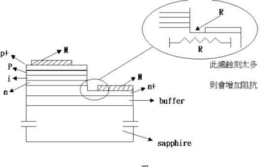
RIE 蝕刻 GaN 的方法雖已普遍的被使用,然而其仍有許多待克服的問題。例如 RIE 蝕刻 GaN 的速度會 shift,因此為求一可靠蝕刻深度在蝕刻到 n type 處均會多蝕刻深 一點,以求品質之一致。以 LED 為例如圖一所示
圖 一
同樣的,精確監控 RIE 蝕刻 GaN 深度除可將元件品質提升外,許多不同結構之元 件量產之良率亦可提升。唯此結果我們可見到數據的散落,RIE 造成的品質之不穩定,
可能是閘極凹槽蝕刻不一致或表面缺陷之原因。
利用光反射光譜監控方法期能即時判斷元件的 PN 接面蝕刻程度。精確的量測 GaN 蝕刻深度至 20 到 100Å 之範圍將能幫助我們了解 RIE 蝕刻的精確度。GaN 再 RIE 蝕刻 後,利用 AFM、STM 對材料表面分析在基礎研究上十分重要。
RIE 蝕刻 GaN 元件可能對 GaN 表面造成的缺陷是不容忽視的,元件的電性特性會 受到很大的影響。例如 p-type Mg doped 的 GaN 在 RIE 蝕刻後表面載子濃度會下降, 即是在 p-type GaN 上作歐姆接觸時阻抗會變大。 因此本計畫擬建立一精確量測及判斷 RIE 蝕刻 GaN 元件 P-N 接面的光學監控方 法。以質譜儀及 IR 反射光譜即時偵測,期能即時判斷元件的 PN 接面蝕刻程度。RIE 蝕刻後即以 STM 分析其表面電性特性,再以 AFM 精確的量測 GaN 蝕刻深度精確的量測 至 20 到 100Å 之範圍,並分析其表面結構。之後再來與質譜儀及 IR 反射光譜之結果比 較。其結果將以評估 IR 反射光譜 in-situ 量測之精確性。 AFM、STM 無法於產業界的設備上整合,在基礎研究上對材料表面分析十分重要, 更可幫助評估元件製程實際生產線作業方法。 為甚麼 GaN 今有如此高的發光效率,在眾說紛紜的情況下,仍是充滿迷思,因為能用 來磊晶 GaN 的基材藍寶石或 SiC,晶格均不是十分的與 GaN 匹配。一般而言,學理上 相信 GaN 發光機制是電子電洞 band to band 再結合,而其熒光頻譜均能以合理的能帶 理論加以 modify 而解釋之。但 GaN 的能帶間隙是 3.5eV,相當於紫外光的能譜,故一般 GaN 發出藍光甚而寬頻帶黃光的發光機制則均是與缺陷或雜質有關。 Illinois 大學電機系莊順連教授在 GaN 的研究中指出,由於製程中的熱處理會影響 GaN 的發光特性,其發光機制與雜質,缺陷有關。亦有學者提出,由於 GaN 與基板的晶 格不匹配,會有許多缺陷產生,而此缺陷可能形成量子點(quantum dot),反而十分幸運 的形成有利於發光的條件,而優於 ZnSe 等之有十分匹配晶格的基板的發光材料。 缺陷可能是形成 GaN 發光機制最有關的原因。與雜質,缺陷有關的原因則不少,從 GaN 長晶開始的原料純度至基板材料原子與磊晶因高溫時的雜質擴散,造成 native 成長出來
的磊晶即是 n-type 的 GaN。晶格的不匹配產生的錯位形成了線(threading)、螺旋(screw)
缺陷,伴隨著點缺陷亦有相當關係。由於是氮化物的關係,許多類似在第四族發生的缺 陷在 GaN 中則因 N 的 passivation(鈍化)。而 N 與缺陷間多半是以空洞相伴,形成點缺
陷不致造成嚴重的 breakdown 問題。空洞伴隨著的點缺陷在 GaN 中分佈有 VN、VGa的缺陷,
依磊晶生長條件不同而存在,VG會穩定得在 N-rich 的 GaN 中存在,即是 n-type 的 GaN。
VN會穩定得在 Ga-rich 的 GaN 中存在,即是 p-type 的 GaN。亦可能由於生長的條件不穩
定而 VN、VGa二者同時存於磊晶中。稜角錯位被預期會存於 GaN 中,在 n-type GaN 中是一
個電子陷阱(electron trap),在 p-type GaN 中是一個電洞陷阱(hole trap)。文獻 上的 E2 center 已被多方面探討過,較早的研究指出 E2 可能是一化學雜質的缺陷,來自 C 或 Mg 所形成。最近的研究則指出,E2 center 可以利用 In 的 doping 而有效壓抑。電 子束輻射(Electron Irradiation)亦是常用來活化 p 型 GaN 的方法。研究來自 EI 所引
起的缺陷發現 VN不受電子束輻射影響,而有 NI 及 NGa的缺陷,存在有互相消長之反應 VGa
+ NI → NGa,形成一電子陷阱。
GaN 半導體材料製造元件的製程中 P 型 GaN 半導體系以 Mg 滲質再以熱處理加以活 化。Ni/Au 是目前 GaN 最普遍適用的 P-type ohmic contact 用金屬,但 Ni 的金屬性 質與 Au 並非自然相容,故實際上製造 GaN LED 的 Au/Ni/P-GaN ohmic contact 有許多
關鍵性的技術。 P 型 GaN 的金屬 ohmic 接觸一般在 Au 與 GaN 之間加一層薄的 Ni,並
在含氧的氣氛下加以熱處理,其可能形成歐姆接觸的機制是 Ni 會和氧形成氧化鎳,而在 與 GaN 的 Ga 共結合,伴以空洞傳導電荷,而形成良好的導電接面。
除了 Au 在 Ni 表面上的覆著不易的困難外, Au/Ni 覆膜的歐姆接觸法亦早有國外廠 商申請專利,故本國廠商從事此項製程時,均須閃躲其專利,故亦有廠商將此段製程交 付有專利及技術之工廠代工以解決上述之問題。
另一方面,,國外亦有許多研究機構在 GaN 元件的金屬接觸問題上嘗試以 Au/Pd/Ni (palladium 鈀)的合金來克服,且多用於 laser diode 的研究上,是否亦是由於專利的 問題,而引導研究群對 Pd 合金和 GaN 的歐姆接觸研究其背景不清楚但是其用於 laser diode 上則可見其具有優異的性質,唯 Pd 在世界主要產地為俄國,且產量少,價格貴。 更重要的是不易取得穩定來源,故研究上亦不易進展。縱觀發展至今,雖然高亮度 GaN 藍 光,白光 LED ,甚而 UV 的 laser diode 早已問世,但此關鍵性技術上的基本學理,仍 不清楚。在 GaN 元件製程中,降低 P type GaN 的電阻及有良好的金屬歐姆接觸是提高 GaN 元件品質之重要的關鍵,對 LED 元件之亮度及壽命有很大影響,目前的 GaN LED 光電廠 均在努力改善此一技術。
製造低阻值的 wide-band-gap 半導体薄膜,不論是n type或是 p type均是十分困難, 其主要原因乃是所謂的單極性和中和(compensation)的問題,藍色至紫外光雷射的應用 均由於在P type 的 GaN及 P type的 AlN材料的電阻質太高。低阻值的 wide-band-gap 半 導体製造十分困難的主因乃是離子的低溶解度、低活化效率和是深能階雜質(deep level impurity)產生的載子中和(compensation)的效應。由於die1ectric constant很小,致使 得acceptor或 donor level十分的 deep(約幾百個mev),在室溫下電洞能被激發的密度很 小且僅有acceptor 10-6 的濃度。故提高滲質doping之濃度以增加載子數目及利用各種處 理方法增加其活化效率是降低阻值的必須雙向並重的方向。 在半導體 GaAs 及矽 IC 製程中離子佈植技術一項十分成功之 doping 滲質方法。它可十 分精確得將一定劑量之載子雜質注入至樣品表面下一定深度及位置。由離子佈植所造成 的 damage 缺陷可以經由一定溫度的熱處理予以消除,故而能得到十分低阻值的電子元 件。此項離子佈植技術在近年來亦被提出【1-6】加以多方應用來滲質,以求改善 GaN 的 阻值。目前已有多少了解 GaN 經離子佈植處理後的一些特性,如會有非晶化、形成孔洞、 缺陷經 annealing 後消除不易及離子佈植劑量過高會引起不可消除的缺陷等等,似乎尚 無實用性之結果公諸於世。然而一方面由於離子佈植技術在 GaAs 及矽半導體 IC 製程中 十分成功,而令人抱有決大希望,再則在磊晶成長中滲質之結果仍不理想,且離子佈植 技術且有許多優點,故繼續以離子佈植研發的腳步只有更加速進行。 藍光 GaN LED 是目前世界各國積極投入發展白光源項目中最重要的關鍵光電材料。 國內有二十餘家光電廠商投入。多集中在上中游之磊晶、晶粒製程,其中不乏投資龐大 之廠商從上至中、下游。國內產量在世界上佔有相當份量,而品質亦且具有一流之水準、 價格在國內廠家之惡性削價之情況下,自然在世界上亦具有充分之競爭力。唯環顧美、 日等國 CREE, Nishia 大廠品質與價格可知,加強品質(尤其是亮度)是突破國內惡性競 爭、價格低迷的唯一之途。除了 epi 上加強磊晶片之品質、設計更有效率之元件結構之外, 其中之製程改善是極重要之一環。其中之一製程中,須以 RIE 蝕刻出 n 型之電極。ICP RIE 是目前國內廠商使用來蝕刻的最普遍方法,而製程的精確與否,會影響 GaN LED 的發光 亮度。我們在計畫中提出以 AFM 分析蝕刻深度及以 in -situ 紅外光反射光譜監視在 GaN LED 磊晶膜表面蝕刻 p 型及 n 型 layer 狀況之實驗,目的在提供一可精確量測對 GaN 蝕刻 之監測方法,並配合熱處理研究,以了解蝕刻製程對 GaN LED 蝕刻後的 damage 熱處理恢 復問題,以提高 GaN LED 元件製程之精確度而提升元件之品質。
在本計畫的研究中我們依計畫利用 RF 電源自製一套以 ICP RIE 的電漿耦合離子蝕刻 設備,利將用 HCl 氣體激發成電漿,藉此分解 C–H 鍵分子,在在 GaN LED 的 epi-layer 上進行蝕刻實驗。樣品再以 SEM、FTIR 及微結構拉曼光譜分析蝕刻後之 GaN 薄膜以及其 PL 的發光特性。第一年計畫中原有設計 in-situ 紅外光反射光鐠監視蝕刻之構想,由於 第二年相配合之計畫未核准補助此項 in situ 紅外光反射光鐠監視用的光學附件,而經 過不斷詢價,所須費用在本計畫中實無法負擔而作罷。而在蝕刻深度的精確量度上原計 畫構想係須構置一台 Digital Instrument 的 AFM,然本計畫所獲補助只能購置一雜牌陽 春機型,其功能、解析度不足,無法勝任本計畫之須求。且因適時有南部貴儀中心的 DI AFM 採購計畫,由於不希望資源的重複投資,故在計畫執行過程中我們二度申請變更計畫內 容,而將主力投入利用 micro Raman 及 PL 分析,研究蝕刻製程對 GaN LED 蝕刻後的 damage 熱處理、恢復問題。在蝕刻深度的精確量度擬利用南部貴儀中心之 AFM 設備。最後實驗 結果係以 SEM、FTIR 及利用 micro Raman 及 PL 分析蝕刻、熱處理、恢復製程對 GaN LED 蝕刻後的徵結構變化。 此外由於自製之 ICP RIE 在發展之過程中多次因不暗腐蝕性氣體之特性,由於使用 不當而造成 pump、氣體管線及電容真空計損壞,未能達成蝕刻後 n type 電極歐姆接觸之 研究。以上的多處困難及阻礙使得計畫原有構想無法繼續,而南部貴儀中心之設備採購 進度不如預期,雖終在本計畫的最後階段完成購置,才能提供服務。然本計畫下執行的 同學經多次努力尚未能得到滿意的量測數據。AFM 的分析亦將繼續的做下去。基於研究、 克困難、尋求解決之法,本計畫即在第二次變更計畫內容後,以 ion implantation 之實 驗取代一時不能解決之 ICP RIE 設備損壞,未能繼續實驗的困境。利用 ion implantation 來研究 doping 及表面破壞之復原亦是十分重要的方法。此部分我們經與澳洲合作伙伴協 助在坎培拉的澳洲國立大學電子材料物理與工程系完成一系列的 As ion 在 GaN LED 表面 下 50Ǎ 的離子佈植實驗,並進行了快速熱處理的退火實驗。樣品在 Implantation、RTA annealing 實驗前後均以 FTIR、PL 及 Raman 光譜分析其發光的特性。
研究結果發現蝕刻製程會影響 GaN LED 表面特性。在過於強能量的離子蝕刻下,會 在 GaN LED 表面造成結構性的傷害,而令 GaN 的發光特性衰退,適當之熱處理能令元件 的發光特性恢復,然過度之離子蝕刻後 GaN LED 不能發光,其 damage 的機制尚未明瞭, 本計畫繼續下去將做 TEM 的分析以分析 GaN LED 表面的微結構。
上項困難與尚待完成之工作將由本年正在執行的研究計畫克服後續加以完成。本年 度參與計畫有二位碩士班研究生完成論文,進入國防役及 IC 廠服務。此外我們已將研究 成果中具學術價值的部分完成一篇論文投至國際期刊,以下為本計畫研究結果之重要部 分報告。
五、成果內容:
1. Introduction
Bright white and Blue GaN LED has expected to be one of the most important materials for the future white lighting source. Besides the necessary of a good quality of GaN epitaxial layer, the brightness of GaN LED will be also strongly influent under its processes. Especially, the RIE could lead to a surface damage and subsequently the degradation of its electro-luminescence. Since when the high energetic ions bombard the GaN crystal surface to remove atoms from the crystal surface, parts of ions with higher energy can implant into the surface crystal, collide with inner atoms and eventually break down the atomic bonds and ionize the lattice atoms. Such an etching or implantation process produces damages, such as local electrical defects, non-irradiative recombination states in the crystal. In addition to etching through the ionic bombardment, ion implantation is also one of the useful tools for the doping impurities into semiconductor. Similarly to ionic bombardment, ion implantation produces also damage of the surface crystal of the semiconductor. In general, some of the damages can be recovered through an appropriate annealing treatment. It has been shown a fruitful result for silicon integration circuits doping by implantation using annealing processes. Many groups have also long extensively studied using high energetic ions to bombard the GaN. However, until to now, although many studies on the annealing, damages after implantation into GaN shows unrecoverable deterioration of irradiation. We consider the process of ion implantation has been successful used for GaAs doping. On the other hand GaNAs is a interesting substance model because of its band gap reveals to be narrowed as small amount N in cooperated epitaxial grown into GaAs. This phenomenon is in contrast to GaN with wider band gap. The optoelectronic properties of GaNAs have not yet been quit understood. The contrast proposal is to study the effect of As ion implanted into GaN to form a As poor GaAsN substance. Two possible key point will be cleared that one is that whether As will be a possible dopant implanted into GaN to assist GaN forming a good metal-semiconductor ? The second key point is the effect for doping of As into GaN. Will a narrower band gap for the system GaNAs also be found? An optical property analysis will interest the band gap engineering principle.
In this project we have carried out the following topics for a basic study of the ionic bombardment in two categories between the etching and the doping. For the ionic bombardment leading to an etch effect is the main point of the surface damage and an annealing treatment for the recovering of the crystal surface from damage. The second issue is that by energy higher ionic bombardment the ions will implant into the surface crystal causing a doping effect. Both of the etch and doping need the further annealing treatments for recovering the crystal structure.
1. In the first part we have studied the Cl ionic reactive etch on n type GaN and the damage of surface layer of a GaN LED. To the cooperated AFM analysis has just finished its instrument installation as this project is to end, so we have just continued to carry on the experiments as we keep going on the new project running on the ion implantation study on GaN and the formation of its ohmic contacts.
2. In the second part we studied the effect of As bombardment on GaN surface. The Ga-As and Ga-N are interesting model substances of ternary components systems. GaAs has an energy band of 1.46eV and for GaN is the energy band of 3.5eV. However, the ternary system GaNAs is not well known for its properties. Using the implantation we would like to understand the trend of recovering in GaN with As defects.
etching. The crystal loses its PL irradiative property due to the heavy surface damage through ionic bombardment even after higher temperature and longer annealing. Since GaN surface after annealing can not recover to its original smooth perfect structure, GaN surface plays an important roll for its irradiation.
2. Experimental details
In this work the GaN LED samples are grown from the company South Epitaxy Corporation, Tainan, Taiwan with the commercial D-degree quality for the brightness of 4mW. Samples are cut into small size for RIE experiment. ICP-RIE experiment is performed with a RF coils induced plasma reactive etching method in a homemade reaction chamber with a 2KW power supplier of 13.56MHz radio frequency source. The gas of a mixture of HCl, N2 and Ar gas,
pressure in the range of about 5 x 10⁻³Torr, is induced to generate plasma. A built-in electrode is setup for a negative bias of 200V under the sample holder. Fig.1 shows the experimental scheme of ICP RIE. A strip mask made of steel has been used to produce the etch patterns. GaN samples have been measured by FTIR, and micro-PL before and after etching. Some samples after etching irradiated with rather lower PL intensity and some didn’t irradiate anymore. An annealing treatment has performed for GaN samples in order to investigate the recover effect. After annealing samples are analyzed again.
For ion implantation of As ions into GaN, the experiments were carried out in the Institute of Physics and Engineering for the electronic materials, National University, Canberra, Australia. GaN samples were implanted with As ions with a energy of 100KV and the dose of 2·1014, 2·1015, and 2·1016atoms/cm2. After implantations sample have been annealed in a rapid thermal Annealing equipment for 900C 10min and 1000C 3min. The GaN samples have been analyzed through the micro-Raman spectroscopy and SEM for investigating the changes of its structure. The micro-Raman backscattered spectra in parallel polarization were taken from an Olympus microscope (objective ×100) and excided with a wave length of 325nm form HeCd laser. A series samples are also made for the TEM analysis. However, the whole work needs still more time, and will be completed in the continuous project of this year.
3. Results and discussions
In the following section we shall report some of the results, which are the key points we have submitted to the journal and in conference presented, too. Fig.2 shows the infrared transmittance spectra of the n type GaN layer of the LED sample before and after As ionic bombardment. In the spectrum range of 1250 to 1400 cm-1 is there an absorption respondent to observe, which is absent for the samples after etching of Cl ions. However, due to this broaden peak change it is hard to claim any chemical absorption due to As reaction but an ionic interaction with its surrounding lattice atoms. Such a change has not been observed by the samples of p type GaN epi layer after bombardment. GaN samples after annealing can not be recovered to the earlier transmittance. Where in all the spectra range the transmittance intensities are decreased. That means after bombardment the exceed charge states existed and absorbed more IR light.
ions and following annealed at 900°C 3 min and 1000°C 1min. The FTIR spectra show that the transmittance proportionally decreased after implantation the As ions into GaN. The absorption of IR light represents the orgin center of charges, defects or scattering of the atoms and also surface reflections. In Fig. 2 the effect shows the more implanted As the lower FTIR transmitted. As the surface reflection or roughness can cause a lowering the transmittance, However, the implanted ions makes lots of surface damage, ionization of lattice atoms can reduce the irradiation of the device. The decrease of the broad peak of 500-750 cm-1 indicates the absorption of such defects. A detailed sturdy on the PL can reveal the better understanding of these defects.
Fig. 3 shows the detailed view of the FTIR spectra of fig. 2 from the range of 500 to 560 cm-1. At 520 cm-1 the spectra reveal the transmittance peak in dependent on the doping processes. In fig 2 the changes has been observed for both n and p type GaN epi layers. However, they change in opposite ways. For n type GaN epi layer, it reveals increased transmittance as more dose of As implanted in to GaN. But for p type GaN epi layers, it shows lightly decreased transmittance. For both n- and p type GaN epi layers the 1015 atoms/cm2 doped samples have the largest transmittance. It indicates a structural change for the heavily doping of implantation of 1016 atoms/cm2. It seems that through the heavy dose implantation the surface structure has been destroyed than to be damaged, that the transmittance decreased because of the more been produced defects or charge states. These damages reveal a rapidly decrease of their PL intensity. Especially for the case of 1016 atoms/cm2 heavy doped sample, although the implantation occurred at the position near the surface of some hundreds angstroms depth. Its PL vanished totally even after RTA annealing.
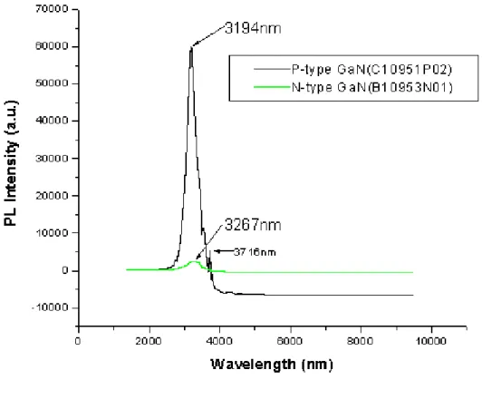
In Fig 4 are shown the PL spectra of the GaN LED before and after etching and annealing. The etching process has removed the p type and MQW layers over the n-layer. After etching the GaN did not emit PL any more. And a RTA process at 1000℃ for 3 min has recovered the surface damage of the n-layer. However, this damage did not be full recovered, that it PL intensity is much lower than that of the origin p-layer. For lower energy ionic etch could not remove any GaN layer, but high energy ionic etch leads to the strong bombardment of ions on the GaN surface and to lowering its PL. The etch process shows to be an important technique for the LED process for the device quality. Beside the bias the other factor to increase the etching rate but not damage the GaN surface is an key point for the next research issue.
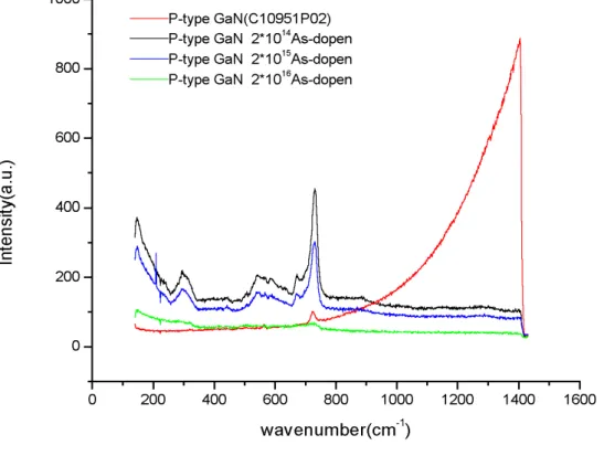
Fig. 5 shows Raman spectra of p type GaN samples before and after implantations of As ions and annealing. The peaks at 732cm-1 correspond to Ga in lattice vibration. Ga is rather heavier than N atoms in lattice. After collision of Ga that Ga-N bonds broken produce the internal stress and defects center, which distort the lattice structure and reveals to the non irradiative of GaN. Although GaN LED structure contains MQW as emit center, the near surface defects after ionization and distortion depress the recombination of electrons and holes in MQW through the implantation process. In Fig. 5 we observe that the peak of 732cm-1 decreased as its PL intensity disappeared and reemitted after recovered annealing. Correlated FTIR spectra reveal the same effect for the absorption peak at 510cm-1as shown in Fig. 2.
PL spectra of GaN samples show that only by lightly doping can the PL increased after annealing recovered, but cannot come back to its original intensity. Raman spectra reveal a peak at 732cm-1be corresponded to the structure of Ga in lattice, which has also been shown in Fig 4 for the correlated PL spectra. For heavily doping of As into GaN will the RTA process not be recovered.
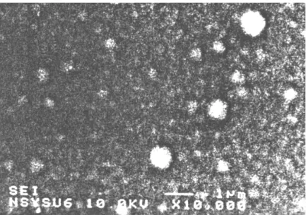
and annealing at 1000℃ for 3 min, in which big size particles produced after annealing. For such a heavy doping of As, the surface of GaN epi layer was fully damaged and its crystal lattice can not be recovered again. After annealing the surface of GaN became rough and some particles with big or small size are eliminated. The compositions of these particles are mainly of As. For such an elimination of As to form particles shows that the GaN lattice is very strongly bonded and repulse the foreign impurity atoms strongly. Surprisely were the As ions migrated together to form the particles even as large as 1μm . The similar phenomenon has been observed for phosphor implanted doping into diamond. Its formation mechanism is not clear for the date understanding, and this phenomenon needs more investigation.
In our study we found that GaN reveals strong bonding of its lattice and cannot be gradually etched from surface atomic layer by layer. Higher energy bombardment will be needed to etch or implant into GaN. This process causes the damage of GaN surface. For implantation of As into GaN the surface will be damaged and through RTA annealing to be recovered. However, PL spectra of the GaN LED after implantation and annealing show only by lightly doping can the PL increased after annealing recovered, but neither come back to its original intensity. PL spectra correlated to Raman results reveal a peak at 732cm-1 be corresponded to the structure of Ga in lattice. A surface damage of this bond causes PL rashly decrease.
4. Conclusions
We have reported the study of the effect of Cl etching and implantation of As into GaN LED. The surface of GaN LED shows an unrecoverable damage through the PL investigation. Raman spectra shows that an Ga bond at 732 cm-1 corresponds to the irradiation of GaN, which decreased rashly after implantation and increased after annealing. SEM micrograph reveals a production of As particles in GaN after annealing. For further understanding of such phenomenon needs more investigation.
5. Acknowledgement
The authors thank Miss. C. S. Chen, Department for Materials Engineering, National Sun Yat-sen University, Kaohsiung for her kindly technical assistance of the SEM measurement. The authors further gratefully acknowledge financial support from the National Science Committee under the projects Nr NSC 90-2112-M-110-011 and NSC 91-2112-M-110-018.
6. References
[1]X.A.Cao,S.J.Pearton,G.T.Gang,A.P.Zhang,F.Ren,R.G.Wilson,J.M.Van Hove,“Creation ofhigh resistivity GaN by implantation ofTi,O,FeorCr”J.Appl.Phys.87,1091(2000) [2]S.O. Kucheyev, J.S. Williams, J. Zou, G.Li, C. Jagadish,A.I.Titov,”Effectofion specison
implantation-produced disorderin GaN atliquid nitrogen temperature”NuclearInstrument& Method in Phys. Research B, 190 (2002)782
[3]J.A.Fellows,Y.K.Yeo,R.L.Hengehold,D.K.Johnstone“Electricalactivation studies of GaN implanted with Sifrom low to high dose”,Appl.Phys.Lett.80,1930(2002)
[4]S.O.Kucheyev,J.S.Williams,J.Zou,C.Jagadish,G.Li“Theeffectofion mass,energy,dose, flux and irradiation temperatureon implantation disorderin GaN”,Nuclear Instrument & Method in Phys. Research B, 178 (2001)209
[5]S.J.Pearton,J.C.Zolper,R.J.Shul,F.Ren “GaN:Processing,defects,and devices”J.Appl. Phys. 86, 1(1999)
[6]S.O.Kucheyev,J.S.Williams,S.J.Pearton “Ion implantation into GaN”Materials Sci. Eng. Reports 33(2001)51
[7] S.O. Kucheyeva, J.S. Williams, S.J. Pearton, Materials Science and Engineering, 33 (2001) 51-107
[8] B. J. Pong, C. J. Pan, Y. C. Teng, G. C. Chi, W.-H. Li, and K. C. Lee, ansd Chih-Hao Lee , J. Appl. Phys. 83(2002) 5992-6
Figure Captions
Fig. 1 Experimental scheme of ICP RIE
Fig.2 FTIR spectra of n type epi layer of GaN LED under bombardment of As ions
Fig.3 FTIR spectra of both n and p type epi layer of GaN LED under bombardment of various concentration of As ions
Fig. 4 PL spectra of GaN LED sample before and after etching up the n type layer and annealing
Fig. 5 Raman spectra of p type GaN samples before and after implantations and annealing
Fig. 6 SEM micrograph of the GaN sample implanted with 1017atoms/cm2of As and As particles produced after annealing of 1000ºC 3 min.
15
17
Fig.3 FTIR spectra of both n and p type epi layer of GaN LED under bombardment of various concentration of As ions
19
Fig. 6 SEM micrograph of the GaN sample implanted with 1017atoms/cm2of As and As particles produced after annealing of 1000ºC 3 min.