AN OPTIMIZATION-BASED LOW-POWER VOLTAGE SCALING TECHNIQUE USING
MULTIPLE SUPPLY VOLTAGES
E-Jong Yeh and Sy-Yen Kuo
Department
o f
Electrical Engineering, National Taiwan University, Taipei, Taiwan
[email protected], [email protected]
ABSTRACT
In this paper, we proposed a voltage scaling technique with multiple supply voltages for low-power designs. We consid- ered the path sensitization as well as releasing the clustering constraint applied in the CVS (Clustered Voltage Scaling) technique. Our technique operates the gates with the low- est feasible supply voltages and then uses an existing path selection algorithm for optimization. Experiments are con- ducted on the ISCAS85 benchmarks and the results show that about 20% power on average can be further reduced by our technique in comparison with the CVS technique.
1. INTRODUCTION
Power consumption is one of the most significant param- eters in VLSI designs. In a CMOS digital circuit, power consumption is dominated by dynamic power, which is pro- portional to the square of the supply voltage. As a result voltage scaling is evidently an effective technique in power reduction and was employed by many researchers.
The conclusion of [ 11 provides us a simple rule in power reduction, i.e. operate a circuit as slowly as possible with the lowest possible supply voltage. The most popular voltage scaling technique is to operate all the gates in a circuit with a reduced supply voltage that is limited by the critical paths. However, the gates that are not on critical paths could oper- ate slower with lower supply voltages. Consequently two or more supply voltages were employed in previous works.
In [2]-[4], the power consumption was reduced with multiple supply voltages at function level, where the effect of interconnections between entities with different supply voltages was insignificant and could be ignored. In [5] and [6], the power consumption was reduced with two supply voltages at gate level, where level converters were inserted to prevent the static current when the gates with lower sup- ply voltages drive the gates with higher supply voltages.
To reduce the complexity of physical layout with mul- tiple supply voltages, gates of the same supply voltage are This research was supponed by National Science Council. Taiwan.
under the Grant NSC 87-2213-E259-007.
clustered at circuit topology in [5] and [6]. However, gate clustering can be done at the early phase of physical layout. Therefore, we released the clustering constraint, applied in [5] and [6], and proposed a multiple-voltage scaling tech- nique to freely exploit the timing slacks at gate level in this paper.
2. DEFINITIONS AND TERMINOLOGIES We first give some basic terms, which can be found in [I I], and use them throughout this paper.
A pntli P = (Go, fo,
G I ,
f l,
. .. ,
f r n - l ,G,)
in a com-binational circuit is an alternating sequence of wires and gates. Wire
f,,
05
i5
m - 1, is called an on-input ofP
which connects gateG,
to gate G,+1. A wire is called a side-input of if it is connected to G Vf l but is not origi- nated from G,.
A priniary input vector' is a vector of logic values at all the primary inputs. Wire
f ,
which is connected to gate G. is considered to dominateG
if the stable value and the stable time ofG
are determined by those of f. A path is activated by a primary input vector if each on-input of the path dom- inates its connected gate when the input vector is applied.A path which can be activated by at least one primary input vector is defined as a seizsitixddc path. On the con- trary, a path which will never be activated by any primary input vector is called a false path. The criticnl paths are the longest sensitizable paths in a circuit.
The slack of a gate
G,
denoted by .5(G), is defined as the maximum increase in delay that G may have under the timing constraint.3.
PATH SELECTION ALGORITHMS The actual delay of a combinational circuit is defined as the delay of its longest sensitizable paths instead of that of its longest paths. Therefore, it is pessimistic to reduce the de- lays of all long paths in a circuit for performance optimiza- tion without taking path sensitization into account. Here a long path means that its delay is larger than the timing con- straint of the circuit.v-535
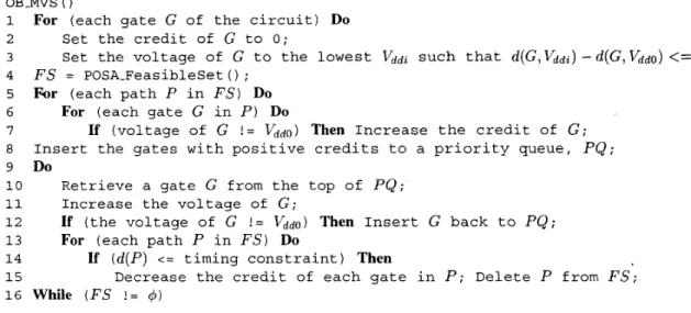
0-7803-6685-9/0 1/$10.0002001 IEEEOB-MVS ( )
1 For (each gate
G
of the circuit)D o
2 Set the credit ofG
to 0 ;3 Set the voltage of
G
to the lowest Vddi such thatd(G,V&)
-
d(G,VddO)
<=
s(G);4
F S
= POSA-Feasibleset ( ) ;5 For (each path
P
inF S ) Do
6 For (each gateG
inP ) Do
7
If
(voltage ofG
! = V&o) Then Increase t h e credit ofG ;
8 Insert the gates with positive credits t o a pri0rit.y queue, P Q ;9
Do
10 Retrieve a gate G from the top of
PQ;
11 Increase the voltage ofG;
1 2 If (the voltage of
G
! = Vddo) Then InsertG
back to P Q ;13 For (each path
P
inF S ) Do
14 If
(d(P)
<= timing constraint) Then15 Decrease the credit of each gate in
P ;
DeleteP
fromF S ;
1 6 While ( F S ! =4)
Figure 1 : The optimization-based algorithm for multiple-voltage scaling.
Several path sensitization criteria have been proposed to estimate the delay of a circuit including the exact criterion, the loose criterion, the BMCD criterion [7], the DYG cri- terion [SI. the PCD criteriori [9], the viable criterion 1131, the
BZ criterion [IO], and the dynamic criterion [l I]. From
the timing verification point of view, a path sensitization cri- terion is considered to be “correct” if the estimated circuit delay is never shorter than the actual delay of the circuit. Certainly, a criterion is more accurate if the estimated delay is closer to the actual delay of the circuit.The objective of path selection algorithms is to select a set of paths for performance optimization techniques. The cost of performance optimization usually depends on the number of long paths selected to be shortened. Generally speaking. the more long paths need to be shortened, the more expensive the optimization will be. As a consequence the number of selected paths should be as small as possible.
As illustrated in [11]-[13], most long paths in a com- plex circuit are actually false. Furthermore, a significant portion of long false paths do not need to be shortened [ 141. We may need only to shorten long sensitizable paths in or- der to meet the timing constraint. However, when all the long sensitizable paths are shortened. a long false path may become sensitizable. On the other hand, some long sensi- tizable paths may not need to be selected for optimization. These problems were tackled in [14] and two selection al- gorithms, vector-oriented and path-oriented, were proposed. For a circuit with many primary inputs, the vector-oriented algorithm may not be feasible since there are too many input combinations. Consequently, the path-oriented selection al- gorithm proposed in [ 141 was adopted in our optimization algorithm.
4. THE PROPOSED ALGORITHM
Now, we can formulated the problem we‘d like to solve in this paper as:
Given a combiriatioizal circuit with a timing coristrain t arid a set of supply voltages, assign the supply voltages to tlie gates in the circuit to minimize the total power consump ~
tioii of tlie circuit.
The basic idea of our algorithm is to operate the gate:; with the lowest feasible supply voltages according to their slacks. Such voltage assignment evidently achieves the lower bound of the formulated problem and the delay of the circuit may be more than the given timing constraint. Therefore, a
path selection algorithm is applied to select a set of long paths for performance optimization. According to the
se-
lected long paths, we can determine the critical order of the gates. Based on the critical order, we increase the supply voltages of the gates in order until the delays of all selected long paths are no more than the given timing constraint.The proposed algorithm, OBMVS ( ) , is shown in Fig- ure 1. The given supply voltages are arranged in descending order and are labeled Liddo, .
.
.,
L 5 d n if the number of the given supply voltages is ( n+
1). Lines 1-3 reset the credits of all gates and operate the gates with their lowest feasible supply voltages. Credit is used to represent the crit- ical order of gates. Line 4 calls POSA-Feasibleset ( ) , which can be found in [14], to obtain a set of long path:;, F S , for optimization. Lines 5-7 set the credits of the gates based on the selected paths inF S .
Next, the gates withpos-
itive credits are inserted into a priority queue,PQ,
in line 8. The priority queue arranges a data structure such that thegate with the maximum credit can be easily retrieved. Lines 9-16 optimize the circuit by increasing the supply voltages
to
V&‘,
its rising delay is estimated byVi,
( v d d-
& h p ) 2‘dd
(v&
-
K h p )of the most critical gates until the timing constraint is met.
=
T d L H x 2 ’ (2)I2
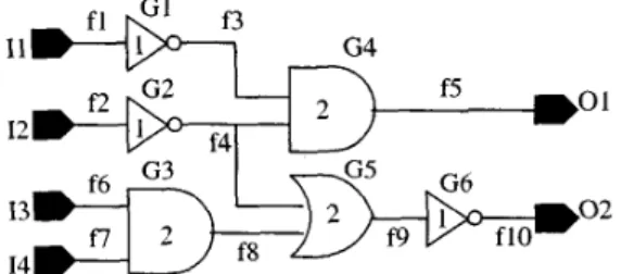
f10 14
Figure 2: An example for the illustration of the proposed algorithm.
Take Figure 2 as an example. Assume that 3 supply voltages are given, the delays of an AND gate or an OR gate at these 3 voltages are 2, 4 and 6 time units respectively, and those of a NOT gate are 1, 2 and 3 time units. In the beginning, the slacks of G1 and G4 are 2 time units, and that of G2 is 1 time unit. So, the supply voltage of G1 is set to I/&>. and those of G2 and G4 are set to V d d l . After
such voltage assignment. the delay of the circuit becomes 7 time units while the original delay is 5 time units. Next,
P O S A - F e a s i b l e s e t ( ) is applied and 2 paths, (11, f 1, G I , f3, G4, f5, 01) and (12, f 2 , G2, f4, G4, f 5 ,
Ol),
are selected for optimization. Based on these 2 paths, the credit of G4 is set to 2 and those of G1 and G2 are set to1 . Therefore. the supply voltage of G4 is set back to V d d O .
Then, the delays of these 2 selected paths are no more than 5 time units and the circuit is optimized.
5. EXPERIMENTAL RESULTS
We have implemented our algorithm in C on a Pentium-I1 450 PC running Linux (RedHat 6.0) with 128MB memory, and performed experiments on all the ISCAS85 circuits. In
addition, we implemented the CVS technique for compari- son.
In our experimental cell library, the length of each MOS is 0.8pm, the width of each PMOS is 16.8,um and the width of each NMOS is 8pm. Using HSPICE to simulate each gate in the cell library, we obtained the parameters for tim- ing and power analysis.
The rising delay
T ~ L H
of gate G is estimated by T ~ L H = (rise ao)+
(rise a l ) x Gout, (1) where Couf is the sum of the output capacitance of gate G and the input capacitances of its fanouts. The falling delay is estimated similarly. If the supply voltage of a gate is scaledFor the power analysis, the activity factor of each pri- mary input is assumed to be 0.5, and the activity factors of other gates are computed accordingly. Then, the power consumption Pd of a gate with supply voltages V d d ’ , can be estimated by
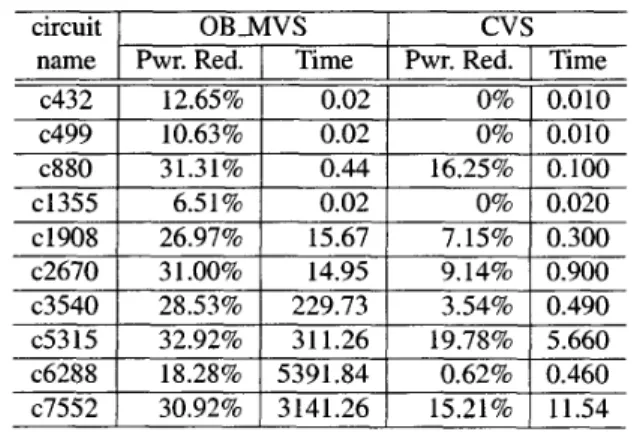
(3) When 2 supply voltages are given, we can compare the results of the O B N V S technique with those of the CVS technique. The O B M V S technique can identify the false paths as well as releasing the clustering constraint which was applied in the CVS technique. Consequently, a signifi- cant improvement in the OBMVS technique over the CVS technique is expected. In Table 1, two supply voltages, 5V and 4V, are given for voltage scaling. We can see that the results of O B M V S are all much better than those of CVS. On average, the power reduction of OB MVS is 22.97%, while that of CVS is 7.17%. In Table 2, where 5V and 3V are applied for voltage scaling, the results of OBAIVS are even better than those of CVS. The average power reduction of OBh4VS is 32.28%, while that of CVS is 8.99%.
The results of the O B M V S with 3 supply voltages, 5V, 4V and 3V, are shown in Table 3 and are compared to the lower bounds which are obtained from lines 1-3 of OB-MVS. The third column of Table 3 shows the total negative slacks at the lower bounds, which represent the tightness of the lower bound. We can find that the power reductions of OB-MVS are close to those of the lower bounds with small total negative slacks.
1 2
Pd = - x f x
a
x(v&)2
6. CONCLUSIONS
In this paper, we released the clustering constraint applied in the CVS technique and proposed a voltage scaling tech- nique with multiple supply voltages. Our technique oper- ates the gates with the lowest feasible supply voltages and then uses an existing path selection algorithm for optimiza- tion.
From the experimental results, we can see that our al- gorithm adds another 19.55% power reduction on average over that of the CVS technique. Furthermore, the power re- ductions of our algorithm are close to the lower bounds with small total negative slacks.
7. REFERENCES
[ I ] Chandrakasan A.P., Sheng S. and Brodersen R.W. “Low-Power CMOS Digital Design”. ZEEE Jouninl of Solid-state Circuits, pages 473434, Apr. 1992.
Table 1: Comparisons between OBlMVS and CVS with 2 supply voltages, 5V and 4V.
circuit name
O B N V S
cvs
Pwr.Red.
I
TimeI
Pwr.Red.I
TimeI cl355 6.51% c2670 c3540 31.00% 14.95 9.14% 0.900 28.53% 229.73 3.54% 0.490 c5315 c6288 c7552 32.92% 311.26 19.78% 5.660 18.28% 5391.84 0.62% 0.460 30.92% 3141.26 15.21% 11.54 circuit name O BM V S
cvs
Pwr.Red.
I
TimeI
Pwr. Red.I
Timec2670 ~ 3 5 4 0 c5315 43.06% 107.55 18.58% 0.880 39.72% 581.18 5.67% 0.460 52.07% 1125.43 29.66% 4.820 c6288 c7552 I I I I I 18.84% 8186.79
I
1.69% 0.440 42.40% 12456.35I
10.57% 5.860V-538
circuit name ~ 4 3 2 c499 ~ 8 8 0Raje S. and Sarrafzadeh M. “Variable Voltage Scheduling”. Proceedings ISLPD, Apr. 1995, pages 9-14.
Chang J.M. and Pedram M. “Energy Minimization Using Multiple Supply Voltages”. IEEE Transactions on VLSI Systems, pages 436-443, Dec. 1997. Manzak A. and Chakrabarti C. “A Low Power Scheduling Scheme with Resources Operating at Mul- tiple Voltages”. IEEE Iiztenzatioiial Symposium on Circuits and Systems, Jun. 1999, pages 354-357. Usami K. and Horowitz M. “Clustered Voltage Scal- ing Technique for Low-Power Design”. Proceedings ISLPD, Apr. 1995, pages 3-8.
Yeh C.W., Chang M.C., Chang S.C. and Jone W.B. “Gate-Level Design Exploiting Dual Supply Voltages for Power-Driven Applications”. Proceedings Design Automation Conference, Jun. 1999. pages 68-7 1.
Benkoski J., Vanden Meersch, E., Claesen L.J.M. and De Man, H. “Timing Verification Using Statically Sensitizable Paths”. IEEE Traizsactions OIZ Coniputer-
Aided Design, pages 1073-1084, Oct. 1990.
Du D., Yen H. and Ghanta S. “On the General False Path Problem in Timing Analysis”. Proceedings De- sign Automation Coifererice, Jun. 1989, pages 555- 560.
Perremans S., Claesen L.J.M. and De Man H. “Static Timing Analysis of Dynamically Sensitizable Paths”. Proceedings Design Autoination Conference, Jun.
1989, pages 568-573.
Brand D. and Iyengar Y. “Timing analysis using func- tional analysis”. IBM Thomas J. Watson Research Center, Technical Report, 1986.
Chen H.C. and Du D.H.C. “Path Sensitization in Crit- ical Path Problem”. IEEE Traizsactiorts on Conzputer- Aided Design, pages 196-207, Feb. 1993.
Devadas S., Keutzer K. and Malik S. “Delay com- putation in combinational logic circuits: Theory and algorithms”. Iitteniatioiial Coilference on Coinputer- Aided Design, 1991, pages 176179.
McGeer P. and Brayton R. “Efficient algorithms for computing the longest viable path in a combinational network”. Proceedings Design Autoinatioii Coifer- ence, Jun. 1989, pages 561-567.
Chen H.C., Du D.H.C. and Liu L.R. “Critical Path Se- lection for Performance Optimization”. IEEE
Trans-
actions 011 Contputer-Aided Design, pages 185-195,Feb. 1993.
LB O B N V S
21.8690 -62 20.26% 0.16
18.90% -84 17.49% 0.88
56.46% -441 48.27% 14.57 Pwr. Red. Slack Pwr. Red. Time
c1355 ~ 1 9 0 8 11.58% -76 10.76% 1.73 51.22% -2452 39.42% 268.60 ~ 2 6 7 0 ~ 3 5 4 0 ~ 5 3 1 5 ~ 6 2 8 8 ~ 7 5 5 2 57.05% -1840 46.69% 379.83 54.53% -7689 42.59% 2435.34 61.58% -5904 53.81% 3849.79 55.87% -48989 22.40% 31062.83 60.61% -14251 45.51% 40073.60