IEEE ELECTRON DEVICE LETTERS, VOL. 34, NO. 5, MAY 2013 677
Origin of Hopping Conduction in
Graphene-Oxide-Doped Silicon
Oxide Resistance Random
Access Memory Devices
Kuan-Chang Chang, Rui Zhang, Ting-Chang Chang, Senior Member, IEEE, Tsung-Ming Tsai, J. C. Lou,
Jung-Hui Chen, Tai-Fa Young, Min-Chen Chen, Ya-Liang Yang, Yin-Chih Pan, Geng-Wei Chang,
Tian-Jian Chu, Chih-Cheng Shih, Jian-Yu Chen, Chih-Hung Pan, Yu-Ting Su, Yong-En Syu,
Ya-Hsiang Tai, and Simon M. Sze, Life Fellow, IEEE
Abstract— In this letter, a double-active-layer (Zr:SiO
x/
C:SiO
x)
resistive
switching
memory
device
with
a
high
ON
/
OFFresistance ratio and small working current (0.02 mA),
is presented. Through the analysis of Raman and Fourier
transform infrared spectroscopy spectra, we find that graphene
oxide exists in the C:SiO
xlayer. It can be observed that
Zr:SiO
x/C:SiO
xstructure has superior switching performance
and higher stability compared with the single-active-layer
(Zr:SiO
x) structure, which is attributed to the existence of
graphene oxide flakes formed during the sputter process. I–V
characteristics under a series of increasing temperature were
analyzed to testify the carrier hopping distance variation, which
is further verified by our graphene oxide redox reaction model.
Index Terms— conduction, graphene oxide, hopping, redox
reaction, resistance random access memory (RRAM).
I. I
NTRODUCTIONT
O SURMOUNT the technical and physical limitation
issues of conventional charge-storage-based memories
Manuscript received December 19, 2012; revised February 20, 2013; accepted February 26, 2013. Date of publication March 27, 2013; date of current version April 22, 2013. This work was supported by the National Science Council of the Republic of China under Contract NSC-101-2120-M-110-002, and Contract NSC 101-2221-E-110-044-MY3. The review of this letter was arranged by Editor T. San.
K. C. Chang, T. M. Tsai, Y.-C. Pan, T.-J. Chu, and C.-H. Pan are with the Department of Materials and Optoelectronic Science, National Sun Yat-Sen University, Kaohsiung 80424, Taiwan.
R. Zhang and J. C. Lou are with the School of Software and Microelec-tronics, Peking University, Beijing 100871, China.
T.-C. Chang, M.-C. Chen, J.-Y. Chen, Y.-T. Su, and Y.-E. Syu are with the Department of Physics, National Sun Yat-Sen University, Kaohsiung 80424, Taiwan, and also with the Advanced Optoelectron-ics Technology Center, National Cheng Kung University, Taiwan (e-mail: [email protected]).
J.-H. Chen and C.-C. Shih are with the Department of Chemistry, National Kaohsiung Normal University, Kaohsiung, Taiwan.
T.-F. Young and Y.-L. Yang are with the Department of Mechanical & Electro-Mechanical Engineering, National Sun Yat-Sen University, Kaohsiung 80424, Taiwan.
G. W. Chang and Y. H. Tai are with the Department of Photonics and the Institute of Electro-Optical Engineering, National Chiao Tung University, Hsinchu 300, Taiwan.
S. M. Sze is with the Department of Physics, National Sun Yat-Sen Univer-sity, Kaohsiung 80424, Taiwan, and also with the Department of Electronics Engineering, National Chiao Tung University, Hsinchu 300, Taiwan.
Color versions of one or more of the figures in this letter are available online at http://ieeexplore.ieee.org.
Digital Object Identifier 10.1109/LED.2013.2250899
[1]–[6], the resistance random access memory (RRAM) is
con-structed of an insulating layer sandwiched by two electrodes.
This structure is a great potential candidate for next-generation
nonvolatile memory due to its superior characteristics such
as lesser cost, simple structure, high-speed operation, and
nondestructive readout [7]–[16].
Recent years have witnessed many breakthroughs in the
research on graphene as well as a significant advance in
the mass production of this material. This one-atom-thick
fabric has many supreme properties, like extreme mechanical
strength and high electronic and thermal conductivities.
In our research, double resistive switching layers with a
sandwiched structure of Pt/Zr:SiO
x/C:SiO
x/TiN were
fab-ricated. Meanwhile, single-resistive-switching-layer RRAM
(Pt/Zr:SiO
x/TiN) was also fabricated so as to make a
com-parison. From the analysis of Raman and Fourier transform
infrared spectroscopy (FTIR) spectra, graphene oxide was
found, and that was the reason why Zr:SiO
x/C:SiO
xstructure
showed better performance of resistive switching
characteris-tics and had lower forming voltage.
As hopping conduction mechanism was found in current
fitting of Zr:SiO
x/C:SiO
xRRAM, I
−V measurement under
a series of increasing temperature was performed to further
obtain carrier hopping distance. Meanwhile, the hopping
dis-tance variation was demonstrated by our graphene oxide redox
reaction model.
II. E
XPERIMENTALS
ETUPThe experimental specimens were prepared as follows. For
the single-active-layer specimen, the Zr:SiO
xthin film (around
20 nm) was deposited on the TiN/Ti/SiO
2/Si substrate by
cosputtering with the pure SiO
2and Zr targets. However, for
the double-resistive-switching-layer specimen, first a C:SiO
xfilm (around 6 nm) was deposited by cosputtering with the
SiO
2and C targets. Then the layer of Zr:SiO
x(around
14 nm) was deposited with the same RF power, argon ambient
and working pressure as the antecedent single-Zr:SiO
x-layer
specimen
Ultimately, the Pt top electrode of 200 nm thickness was
deposited on both specimens by DC magnetron sputtering.
678 IEEE ELECTRON DEVICE LETTERS, VOL. 34, NO. 5, MAY 2013
Fig. 1. Blue and red curves are the resistive switching characteristics of Zr:SiOxfilm and Zr:SiOx/C:SiOxfilm, respectively. The current of Zr:SiOx/
C:SiOxfilm is reduced on both high resistance state (HRS) and low resistance
state (LRS). The figure on bottom left is a forming curve, which shows that Zr:SiOx/C:SiOx film has smaller forming voltage.
The entire electrical measurements of devices with the Pt
electrode of 250-
μm diameter were performed using Agilent
B1500 semiconductor parameter analyzer. Besides, FTIR and
Raman spectroscopy were used to analyze the chemical
com-position and bonding of these insulator materials, respectively.
III. R
ESULTS ANDD
ISCUSSIONThe “forming process” is required to activate all of the
RRAM devices, using DC voltage sweeping with a
com-pliance current of 10
μA. Compared with Zr:SiO
xRRAM,
Zr:SiO
x/C:SiO
xRRAM devices have smaller forming voltage
around 5–7 V (inset of Fig. 1), and the working current of the
Zr:SiO
x/C:SiO
xRRAM devices in both low-resistance state
(LRS) and high-resistance state (HRS) is lower than that of
the Zr:SiO
xdevices (Fig. 1).
To investigate the interesting phenomena, we utilized the
material spectra analyses to find out the reason of working
current reduction and better stability. The C:SiO
xfilm was
analyzed by Raman spectroscopy, from which we found
typ-ical graphene oxide Raman spectra which comprised of a
higher G band peak and a lower D band peak (Fig. 2) [17].
In order to further testify the existence of graphene oxide and
find its chemical bonding type, FTIR was used to analyze
the C:SiO
xfilm. Graphene-oxide-coupled OH peak can be
observed at the wave number of 3665 cm
−1, as shown in the
top right FTIR spectra of Fig. 2.
Through current fitting, we found that
single-resistive-switching-layer devices exhibit Poole–Frenkel conduction in
HRS and Ohmic conduction in LRS, while both LRS and HRS
are hopping conduction mechanisms for double-active-layer
devices. Then, we carried out I –V measurement under a series
of increasing temperature, which is shown in Fig. 3(a) for
ONstate and in Fig. 3(c) for
OFFstate. According to the
relation-ship of hopping conduction, J
= q Naυ
0e
−qφT/kTe
qaV/2dkT,
where N , a,
φ
T,
υ
0, and d are density of space charge, mean of
hopping distance, barrier height of hopping, intrinsic vibration
frequency, and film thickness, respectively, we can draw out
Fig. 2. Raman spectra of C sp2 and C sp3 in C:SiOx film. It confirms
the existence of grapheme oxide. The blue curve on upper right is the corresponding FTIR spectra from which grapheme oxide coupling OH peak can be observed at the wavenumber of 3665 cm−1.
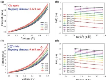
Fig. 3. (a) and (c) ON and OFF state current-voltage characteristics of Zr:SiOx/C:SiOxRRAM under increasing temperature. The calculated hopping
distance is 0.32 and 0.46 nm, respectively. (b) and (d) CorrespondingONand OFFstate activation energy under different voltage.
the curve
φ
T-aV /2d with a vertical axis of In(I
) and a lateral
axis of 1000/T [Fig. 3(b) for
ONstate and Fig. 3(d) for
OFFstate]. As d stands for hopping distance, we calculated from
the curves in Fig. 3(b) and (d) the corresponding hopping
distance for
ONstate and
OFFstate as 0.324 and 0.468 nm,
respectively. The result showed an increase of 0.144 nm in the
hopping distance in HRS as compared with LRS.
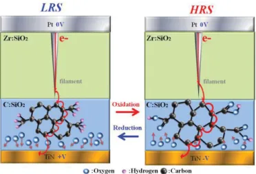
On the basis of the electrical and material analyses, we
proposed a reaction model to explain the transfer of carrier
conduction mechanism of the Zr:SiO
x/C:SiO
xfilm as shown
in Fig. 4. The conductive filament will be formed in the
Zr:SiO
xfilm after the forming process and it will be connected
with graphene oxide flake in the switching region of C:SiO
xfilm. Meanwhile, oxygen-contained groups are removed from
graphene oxide and are driven to the direction of the bottom
electrode. The carrier will hop through carbon atoms within
CHANG et al.: ORIGIN OF HOPPING CONDUCTION 679
Fig. 4. Schematic diagram of graphene oxide redox reaction in Zr:SiOx/
C:SiOx RRAM. The hopping distance variation is due to the stretching of
carbon-carbon bond within the carbocycle.
the carbocycle in the C:SiO
xfilm. If the bottom TiN electrode
is applied with a negative bias to perform a reset process,
oxygen atoms are repelled to the reverse direction of TiN
elec-trode and are absorbed by graphene oxide. With the absorption
of oxygen atoms, carbon-carbon bonds are stretched and
car-bocycle is enlarged, which results in longer hopping distance
of carriers In single-layer RRAM devices, in LRS, electrons
conduct through metal filaments from top electrode to bottom
electrode, and in HRS, electrons conduct through shallow
defects between the tip of the ruptured filament and the
bottom TiN electrode. But in double-layer devices, the
oxygen-contained groups’ absorption and desorption of graphene oxide
result in carbocycle deformation and thus the hopping distance
variation between
ONand
OFFstates in graphene-oxide-doped
silicon RRAM.
IV. C
ONCLUSIONBy cosputtering C and Zr with SiO
2we fabricated a
double-resistive-switching-layer RRAM that has obvious
lower working current and forming voltage. Both FTIR
and Raman spectra confirmed the existence of graphene
oxide. With the absorption and desorption of oxygen atoms,
carbon-carbon bonds within carbocycle are stretched, which
results in hopping distance variation and resistive switch. The
Zr:SiO
x/C:SiO
xstructure has superior switching performance
and higher stability compared with the single-active-layer
(Zr:SiO
x) structure, which is attributed to the redox reaction
of graphene oxide.
A
CKNOWLEDGMENTThis work was performed at the National Science Council
Core Facilities Laboratory for Science and
Nano-Technology in the Kaohsiung-Pingtung area.
R
EFERENCES[1] J. Liu, Q. Wang, S. B. Long, M. H. Zhang, and M. Liu, “A metal/Al2O3/ZrO2/SiO2/Si(MAZOS) structure for high-performance
non-volatile memory application,” Semicond. Sci. Technol., vol. 25, no. 5, p. 055013, May 2010.
[2] D. D. Jiang, M. H. Zhang, Z. L. Huo, Q. Wang, J. Liu, Z. A. Yu, X. N. Yang, Y. Wang, B. Zhang, J. N. Chen, and M. Liu, “A study of cycling induced degradation mechanisms in Si nanocrys-tal memory devices,” Nanotechnology, vol. 22, no. 25, p. 254009, Jun. 2011.
[3] F. M. Yang, T. C. Chang, P. T. Liu, P. H. Yeh, Y. C. Yu, J. Y. Lin, S. M. Sze, and J. C. Lou, “Nickel nanocrystals with HfO2 blocking
oxide for nonvolatile memory application,” Appl. Phys. Lett., vol. 90, no. 22, pp. 222104-1–222104-3, May 2007.
[4] T. C. Chang, F. Y. Jian, S. C. Chen, and Y. T. Tsai, “Developments in nanocrystal memory,” Mater. Today, vol. 14, no. 12, pp. 608–615, Dec. 2011.
[5] F. M. Yang, T. C. Chang, P. T. Liu, U. S. Chen, P. H. Yeh, Y. C. Yu, J. Y. Lin, S. M. Sze, and J. C. Lou, “Nickel nanocrystals with HfO2
blocking oxide for nonvolatile memory application,” Appl. Phys. Lett., vol. 90, no. 22, p. 222104, May 2007.
[6] C. X. Zhu, Z. L. Huo, Z. G. Xu, M. H. Zhang, Q. Wang, J. Liu, S. Long, and M. Liu, “Performance enhancement of multi-level cell nonvolatile memory by using a bandgap engineered high-κ trapping layer,” Appl. Phys. Lett., vol. 97, no. 25, pp. 253503-1–253503-3, 2010.
[7] Y. Wang, Q. Liu, S. B. Long, W. Wang, Q. Wang, M. H. Zhang, S. Zhang, Y. T. Li, Q. Y. Zuo, J. H. Yang, and M. Liu, “Investiga-tion of resistive switching in Cu-doped HfO2 thin film for multilevel
non-volatile memory applications,” Nanotechnology, vol. 21, no. 4, p. 045202, Jan. 2010.
[8] Y. E. Syu, T. C. Chang, T. M. Tsai, Y. C. Hung, K. C. Chang, M. J. Tsai, M. J. Kao, and S. M. Sze, “Redox reaction switching mechanism in RRAM device with Pt/CoSiOx/TiN
struc-ture,” IEEE Electron Device Lett., vol. 32, no. 4, pp. 545–547, Apr. 2011.
[9] K. C. Chang, T. M. Tsai, T. C. Chang, Y. E. Syu, C. C. Wang, S. L. Chuang, C. H. Li, D. S. Gan, and S. M. Sze, “Reducing operation current of Ni-doped silicon oxide resistance random access memory by supercritical CO2 fluid treatment,” Appl. Phys. Lett., vol. 99, no. 26,
pp. 263501-1–263501-4, Dec. 2011.
[10] K. C. Chang, T. M. Tsai, T. C. Chang, Y. E. Syu, K. H. Liao, S. L. Chuang, C. H. Li, D. S. Gan, and S. M. Sze, “The effect of silicon oxide based RRAM with tin doping,” Electrochem. Solid-State
Lett., vol. 15, no. 3, pp. H65–H68, 2012.
[11] T. M. Tsai, K. C. Chang, T. C. Chang, Y. E. Syu, K. H. Liao, B. H. Tseng, and S. M. Sze, “Dehydroxyl effect of Sn-doped silicon oxide resistance random access memory with supercritical CO2 fluid
treatment,” Appl. Phys. Lett., vol. 101, no. 11, pp. 112906-1–112906-4, Sep. 2012.
[12] T. M. Tsai, K. C. Chang, T. C. Chang, Y. E. Syu, S. L. Chuang, S. Lan, C. G. Wei, L. G. Ru, C. M. Chen, H. H. Chun, L. S. Kun, T. Y. Hsiang, G. D. Shin, Y. Y. Liang, Y. T. Fa, T. B. Heng, C. K. Huang, T. M. Jinn, C. Y. H. Wang, and S. M. Sze, “Bipolar resistive RAM charac-teristics induced by nickel incorporated into silicon oxide dielectrics for IC applications,” IEEE Electron Device Lett., vol. 33, no. 12, pp. 1696–1698, Dec. 2012.
[13] T. M. Tsai, K. C. Chang, T. C. Chang, G. W. Chang, Y. E. Syu, Y. En, S. Y. Ting, L. G. Ru, L. K. Hsiao, C. M. Chen, H. H. Chun, T. Y. Hsiang, G. D. Shin, Y. Cong, W. Hao, and S. M. Sze, “Origin of hopping conduction in sn-doped silicon oxide RRAM with supercritical CO2 fluid treatment,” IEEE Electron Device Lett., vol. 33, no. 12,
pp. 1693–1695, Dec. 2012.
[14] Y. T. Li, S. B. Long, M. H. Zhang, Q. Liu, S. Zhang, H. Manhong, Q. Liu, L. Shao, S. Zhang, Y. Y. Wang, Q. Zuo, S. Liu, and M. Liu, “Resistive switching properties of Au/ZrO2/Ag structure for low voltage
nonvolatile memory applications,” IEEE Electron Device Lett., vol. 31, no. 2, pp. 117–119, Feb. 2010.
[15] J. Yao, Z. Sun, L. Zhong, D. Natelson, and J. M. Tour, “Resistive switches and memories from silicon oxide,” Nano Lett., vol. 10, no. 10, pp. 4105–4110, 2010.
[16] A. Mehonic, S. Cueff, M. Wojdak, S. Hudziak, O. Jambois, C. Labbé, B. Garrido, R. Rizk, and A. J. Kenyon, “Resistive switching in silicon suboxide films,” J. Appl. Phys., vol. 111, no. 7, pp. 074507-1–074507-9, Apr. 2012.
[17] N. Hu, Y. Wang, J. Chai, R. Gao, Z. Yang, E. S. W. Kong, and Y. Zhang, “Gas sensor based on p-phenylenediamine reduced graphene oxide,” Sensors Actuat. B. Chem., vol. 163, no. 1, pp. 107–114, Mar. 2012.