This content has been downloaded from IOPscience. Please scroll down to see the full text.
Download details:
IP Address: 140.113.38.11
This content was downloaded on 25/04/2014 at 10:44
Please note that terms and conditions apply.
Nanotip fabrication of zinc oxide nanorods and their enhanced field emission properties
View the table of contents for this issue, or go to the journal homepage for more 2009 Nanotechnology 20 125202
(http://iopscience.iop.org/0957-4484/20/12/125202)
Nanotechnology 20 (2009) 125202 (5pp) doi:10.1088/0957-4484/20/12/125202
Nanotip fabrication of zinc oxide nanorods
and their enhanced field emission
properties
I-Chuan Yao
1, Pang Lin
1and Tseung-Yuen Tseng
21Department of Materials Science and Engineering, National Chiao Tung University, Hsinchu 300, Taiwan
2Department of Electronics Engineering and Institute of Electronics, National Chiao Tung University, Hsinchu 300, Taiwan
E-mail:[email protected]
Received 17 October 2008, in final form 4 February 2009 Published 3 March 2009
Online atstacks.iop.org/Nano/20/125202 Abstract
The ZnO nanorods on ZnO/Si substrates were synthesized by using the low temperature growth aqueous solution method. The chemical and plasma etching treatments were carried out on the as-grown ZnO nanorods to provide the nanorods with various tip angles. The crystal structure and morphology of the ZnO nanorods were examined by x-ray diffraction (XRD), scanning electron microscopy (SEM) and transmission electron microscopy (TEM), respectively. The nanorods grew along the [0001] direction and had various tip angles formed after the above etching processes. The field emission properties of the ZnO nanorods with tip angles of 110◦ and 85◦are: the turn-on electric fields (at the current density of 10μA cm−2) are about 3.03 and 1.70 V μm−1, respectively, while field enhancement factors are 1972 and 3513, respectively. The lifetime measurement result indicates the turn-on field of the ZnO nanostructures reaches a stable value during 1000 cycle times. The enhanced field emission properties are believed to benefit from decreased tip angle of the nanorod emitter.
(Some figures in this article are in colour only in the electronic version)
1. Introduction
One-dimensional (1D) ZnO nanomaterials have recently received much attention for their potential applications in field emission displays, solar cells and other nanodevices [1–3]. So far, among several kinds of fabrication techniques including thermal evaporation, vapor–liquid–solid (VLS) growth [4], metal–organic chemical vapor deposition (MOCVD) [5] and the aqueous solution method [6] used for synthesizing 1D ZnO nanomaterials, aqueous synthesis has the advantages of low temperature, pressure, simple equipment and ambient being achievable for large-area fabrication of different nanostructures. Efficient electron field emission is one of the unique properties of many low-dimensional nanomaterials. In particular, ZnO nanorods have been investigated as electron field emitters due to their high temperature stability, large scale application, high aspect ratio and low working function [7–11]. The recent field emission analysis result of the 1D ZnO
nanomaterials indicates that electrons are more easily emitted from the nanostructures with sharp tips than nanostructures with a uniform diameter. Therefore, it is necessary to control the morphologies of the nanorods for improving their field emission properties. In this paper, we fabricate ZnO nanorods by using the aqueous solution method and develop a new technique to form ZnO nanotip structures from the as-grown ZnO nanorods by using the chemical etching and plasma etching combination process. Based on such a two-step etching process, we can easily adjust the tip angle of the ZnO nanorods.
2. Experimental method
The p-type Si(100) substrate was cleaned by a standard RCA cleaning method and then rinsed in acetone for 30 min to remove native oxide from the surface of the Si substrate. Subsequently, the epitaxial ZnO buffer layer was deposited
Nanotechnology 20 (2009) 125202 I-C Yao et al
(a)
(b)
Figure 1. SEM images of (a) As-grown ZnO nanorods and (b) 2 h chemical etching nanorods.
(a)
(b)
Figure 2. SEM image of (a) the ZnO nanorods after plasma etching and (b) the ZnO nanorods after two-step etching.
by rf sputtering followed by in situ annealing at 750◦C for 30 min. After annealing, the thickness of the epitaxial ZnO buffer layer was about 100 nm, which had a highly preferred orientation along (002) (XRD not shown here). Unless specified, the aqueous synthesis was carried out at 80◦C in a sealed kettle placed in a quartz beaker. The pre-modified substrates were immersed in a precursor solution for 2 h. The precursor solution was prepared by mixing zinc nitrate hexahydrate (Zn(NO3)2·6H2O) with methenamine(C6H12N4)
while keeping their mole ratio at 1:1. After the aqueous synthesis, the nanorods were put in a sealed vessel with various volume ratios of dilute acetic acid at 80◦C for the chemical etching process. The etching time was varied from 1 to 4 h to obtain the nanorods with various tip morphologies, which were then bonded on a sputtering target by carbon tape and exposed to Ar plasma with an rf power of 30 W under a pressure of 5× 10⁻² Torr for 30 s for the plasma etching. The morphology, size distribution and crystal structure of the ZnO nanorods with nanotips were characterized using a field emission scanning electron microscope (FE-SEM, Hitachi S-4700I, Japan) and transmission electron microscope (TEM, JEOL 2010, Japan). The field emission current–voltage (I –V ) curves of both as-grown ZnO nanorods and the nanorods with nanotips were measured at room temperature in the turbopump vacuum chamber at a pressure of 2× 10⁻⁶ Torr. A copper
tip was employed to act as an anode with the tip area of 0.007 09 cm2 and p-type Si covered with ZnO emitters as an
cathode with an area of 1 cm2. We used a micrometer with an accuracy of±0.1 μm to adjust the distance between a copper anode and the tip of the ZnO nanorods, which was 250.0 μm. The field emission properties are affected by the anode area and anode–cathode distance based on Filip’s model [12]. In the present study, we lay emphasis on studying the effect of ZnO tip angle on the emission properties of the ZnO nanorods. Therefore, the copper anode area (0.007 09 cm2)
and anode–cathode distance (250.0 μm) were fixed in this field emission study. The dependence of the field emission current on the anode–cathode voltage was recorded automatically with a Keithley 237 current–voltage analyzer measurement system. The lifetime test was also carried out for the nanorod emitters. The sweeping electric field was from 0.4 to 8.0 V μm−1 and the time interval between cyclings was 5 s.
3. Results and discussion
3.1. Morphology and crystalline structure
The morphologies of as-grown and etched nanorods were observed using FE-SEM and their typical SEM images are shown in figure1. The well-aligned as-grown nanorods have 2
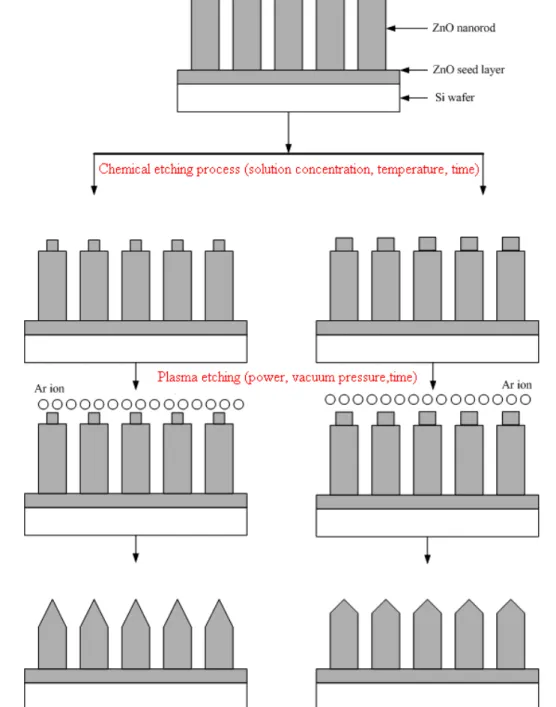
Figure 3. Schematic illustration of the two-step etching process.
perfect orientation perpendicular to the substrate and relatively high cover density (figure1(a)). After chemical etching for 1 h, only a little area near the edge of the nanorods disappears. The etching direction occurs from edge to center with an increased etching time up to 2 h and its image is shown in figure1(b). All these phenomena can be explained by isotropic etching. The six{1¯100} family of planes of the ZnO nanorods possess the same surface energy. Therefore, the six isotropic planes have the same etching rate during the etching process. We can consequently control the tip diameter of ZnO nanorods through using different etching conditions, e.g. etching time, solution concentration and etching temperature. The following plasma etching process is employed to form sharper ZnO nanotips with different tip angles.
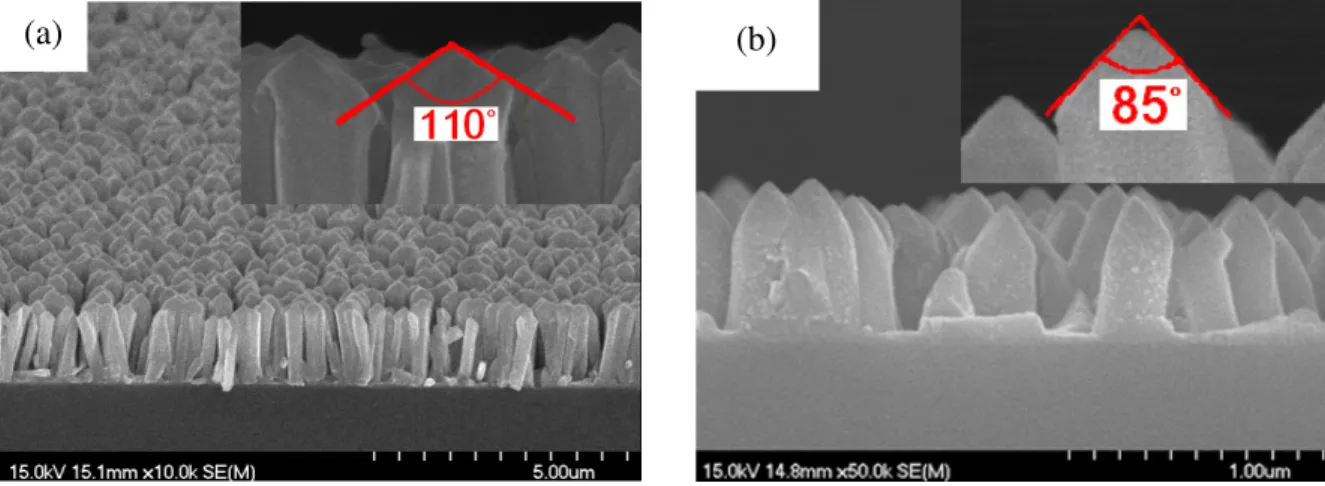
The SEM image of the nanorods after plasma etching treatment with an rf power of 30 W under a pressure of 5×10⁻²Torr for 30 s is shown in figure2(a), indicating that the ZnO acute nanotips are formed after such a plasma treatment and the tip angle is approximately 110◦(inset in figure2(a)). For obtaining smaller tip angles, the combination of chemical and plasma etching processes is employed. Figure 2(b) shows the SEM image of the nanotips obtained by chemically etched for 2 h and then plasma treatment with the same condition as the above-mentioned, indicating that the tip angle of approximately 85◦ can be obtained (inset in figure 2(b)). Our experiment result depicts that using such a two-step etching method, chemical etching for controlling the diameter of nanorods and plasma etching for obtaining acute tips, we
Nanotechnology 20 (2009) 125202 I-C Yao et al
can easily fabricate the nanorods with various tip angles for field emission applications. The schematic description of the two-step etching process is shown in figure3.
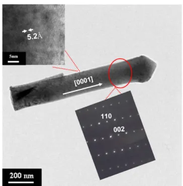
The crystallinity and morphology of the ZnO nanorods after the two-step etching process are investigated by TEM equipped with selected-area electron diffraction (SAED). Figure4shows the TEM and HRTEM images of the nanorods after the above two-step etching process, indicating that the nanorods have a small tip angle of 85◦, which is consistent with the result from SEM observation. It also shows that the preferred growth of the ZnO nanorods is in the [0001] direction. The clear lattice fringes indicate that the interplanar spacing of the (002) c axis of ZnO is 5.2 ˚A (inset in figure4), which is consistent with that of the International center for Diffraction Data (ICDD-2000) database no. 80-0075 of ZnO.
3.2. Field emission properties
The typical field emission properties of the nanorods after various etching treatments are shown in figure 5(a). The emission current–voltage characteristics were analyzed by using the Fowler–Nordheim (FN) equation [13–15] for the field emission measurement: J = A(β2E2/ψ) exp(−Bψ1.5/β E),
where J is the current density, E is the applied field, A = 1.56 × 10⁻¹⁰ (A eV V−2), B = 6.83 × 10⁹(V eV−1.5m−1),
β is a field enhancement factor and ψ is the work function of
the emitter, which is about 5.37 eV for ZnO.β approximately equals 1+ Sdr, where S is dependent on screen effect, d is the distance from anode to cathode and r is the radius of the emitter [12]. The semi-logarithmic J –E plots for the nanorod field emitters are shown in the inset of figure5(a), indicating that the turn-on electric fields of the as-grown, plasma etching and two-step etching emitters are 6.01, 3.03 and 1.70 V μm−1, respectively, at a current density of 10μA cm−2. When the work function of the nanorods is known, the field enhancement factor (β) can be calculated from the slope of the FN plot shown in figure 5(b). The β values are about 946, 1972 and 3513 for as-grown, plasma etching and two-step etching ZnO nanorod emitters, respectively. The average β of the ZnO nanorod emitters is related to the geometry, tip size and number density of the nanorods grown on the substrate. In our case, the emitters with the same nanorod density of 14.75 μm−2were employed, which were prepared through the same processing conditions and the distance between tip and anode plate is kept constant. From SEM and TEM images (figures 1, 2 and 4), we can obtain the aspect ratios of the as-grown, plasma etching and two-step etching emitters as approximately 3.45 ± 0.4, 52.27 ± 6.0 and 56.00 ± 6.2, respectively. As compared with plasma etching and two-step etching emitters, their aspect ratios are approximately equal within measurement errors. Therefore, the copper anode area, anode–cathode distance and aspect ratios are considered to be fixed for plasma etching and two-step etching emitters in this field emission study. We lay the emphasis on studying the effect of tip angles on the field emission properties and found that the smaller tip angle of the nanorods after the two-step etching process would lead to largerβ values and lower turn-on
Figure 4. TEM image of the single ZnO nanorod after plasma
etching: the insets show the corresponding SAED pattern and high resolution TEM image.
fields in comparison with that of the nanorods after only plasma etching, which is obviously confirmed by our experimental results shown above. Figure 5(c) shows the stability of the turn-on field for as-grown, plasma etching and two-step etching nanorod emitters. It can be seen from figure 5(c) that the turn-on fields of the nanorod emitters after two-step etching processes reach more stable values in comparison with those of the as-grown nanorod emitters. The variation of turn-on fields for the as-grown nanorod emitters is more than 1 Vμm−1. We believe that such higher variation of the turn-on fields is due to that the as-grown nanorod emitters might be destroyed by high electric fields. On the other hand, the variation of turn-on fields of the two-step etching nanorod emitters is less than 0.5 V μm−1 during 1000 cycle times, which is much more stable in comparison with that of the as-grown nanorod emitters. Based on the above lifetime measurement results, we would suggest that the nanorod emitters after plasma etching or two-step etching processes, which were bombarded by high energy argon ions, lead to better crystallinity (XRD not shown here) and consequently reach a more stable state. Therefore, those emitters have smaller variation in their turn-on fields.
4. Conclusions
In summary, we successfully fabricated sharp tip structured ZnO nanorods by employing an etching process. Through plasma etching, the 110◦ tip angle nanorods were obtained. We were further able to easily control the tip angle of the nanorods by using the two-step etching process, a combination of chemical etching process and plasma etching process. After such plasma etching and two-step etching processes, the field emission properties of ZnO vertically aligned nanorod emitters 4
(a)
(b)
(c)
Figure 5. (a) J –E curves of the nanorod field emitters. (b) Fowler–Nordheim plots of the nanorod field emitters. (c) Stability test of the
nanorod field emitters.
were significantly enhanced and the stability of their turn-on fields was improved.
Acknowledgment
This work was supported by the National Science Council of ROC under contract no. NSC 97-2221-E-009-150-MY3.
References
[1] Lee C Y, Li S Y, Lin P and Tseng T Y 2006 IEEE Trans. Nanotechnol.5 216
[2] Jayadevan K P and Tseng T Y 2005 J. Nanosci. Nanotechnol. 5 1768
[3] Law M, Greene L E, Johnson J C, Saykally R and Yang P 2005 Nat. Mater.4 455
[4] Li S Y, Lee C Y and Tseng T Y 2003 J. Cryst. Growth 247 357
[5] Lee D J, Park J Y, Yun S Y, Hong S Y, Moon H J, Lee T B and Kim S S 2005 J. Cryst. Growth276 458
[6] Lee C Y, Li S Y, Lin P and Tseng T Y 2005 J. Nanosci. Nanotechnol. 5 1008
[7] Li B Y, Bando Y and Golberg D 2004 Appl. Phys. Lett. 84 3603
[8] Dong L F, Jiao J, Tuggle D W, Petty J M, Elliff S A and Coulter M 2005 Appl. Phys. Lett.87 013110
[9] Wan Q, Yu K, Wang T H and Lin C L 2003 Appl. Phys. Lett. 83 2253
[10] Banerjee D, Jo S H and Ren Z F 2004 Adv. Mater.16 2028 [11] Zhang H, Yang D R, Ma X T and Que D L 2005 J. Phys. Chem.
B109 17055
[12] Filip V, Nicolaescu D, Tanemura M and Okuyama F 2001 Ultramicroscopy89 39
[13] Charbonnier F M, Mackie W A, Hartman R L and Xie T B 2001 J. Vac. Sci. Technol. B19 1064
[14] Liu J P, Xu C X, Zhu G P, Cui Y P, Yang Y and Sun X W 2007 J. Phys. D: Appl. Phys.40 1906
[15] Lee C J, Lee T J, Lyu S C, Zhang Y, Ruh H and Lee H J 2002 Appl. Phys. Lett.81 3648