of traps. Work is in progress to evaluate the capacitance associated with the device to optimize the frequency be-havior.
CONCLUSION
An analytical model for a pseudomorphic MODFET is pre-sented to evaluate its output characteristics. It is shown that the AlGaAsrInGaAs MODFET has better charge control and higher transconductance than the AlGaAsrGaAs MOD-FET. We attribute these improvements to the larger effective conduction band discontinuity, improved confinement of elec-trons in the InGaAs channel, and the better transport prop-erties in the AlGaAsrInGaAs system. The present model is highly suitable for MMIC design as it determines the electri-cal and microwave performance of the device.
REFERENCES
1. H. Morkoc and P.M. Solomon, The HEMT: A superfast
transis-Ž .
tor, IEEE Spectrum 21 1984 , 28᎐35.
2. S. Sen, M.K. Pandey, and R.S. Gupta, A two dimensional I-V model for frequency optimization of heterostructure field effect transistor, Proc Int Conf Comput and Devices for Commun ŽCODEC-98 , Calcutta, India, 1998, pp. 388. ᎐390.
3. S. Sen, M.K. Pandey, and R.S. Gupta, Bandgap discontinuity model for 2DEG density at the AlGaAsrGaAs interface, Proc Asia-Pacific Microwave Conf, 1996, pp. 243᎐246.
4. T.E. Zipperian, L.R. Dawson, G.C. Osbourn, and I.J. Fritz, An In Ga As.2 .8 rGaAs modulation doped strained layer superlattice field effect transistor, IEDM Tech Dig, 1983, pp. 696᎐699. 5. J.J. Rosenberg, M. Benlamri, P.D. Kirchner, J.M. Woodall, and
J.P. Pettit, Pseudomorphic InGaAsrGaAs single quantum well high electron mobility transistor, IEEE Electron Device Lett
Ž .
EDL-6 1985 , 491᎐493.
6. T.E. Zipperian and T.J. Drummond, Strained quantum-well,
Ž .
modulation doped field effect transistor, Electron Lett 21 1985 , 823᎐824.
7. N. Chand, T. Henderson, J. Klem, W.T. Masselink, R. Fischer, Y.C. Chang, and H. Morkoc, Comprehensive analysis of Si doped
Ž .
Al Gax 1yxAs xs 0 to 1 : Theory and experiments, Phys Rev B
Ž .
30 1984 , 4481᎐4492.
Ž .
8. D. Delageleaudeuf and N.T. Linh, Metal- n AlGaAsrGaAs two dimensional electron gas FET, IEEE Trans Electron Devices
Ž .
ED-29 1982 , 955᎐960.
9. Y.H. Byun, Unified charge control model and subthreshold cur-rent in heterostructure field effect transistors, IEEE Electron
Ž .
Device Lett 11 1990 , 50᎐53.
10. M.L. Majewski, An analytical DC model for the modulation doped field effect transistor, IEEE Trans Electron Devices ED-34 Ž1987 , 1902. ᎐1909.
11. K.-W. Liu and A.F.M. Anwar, A self consistent calculation of the small signal parameters for AlGaAsrGaAs and
AlGaAsrIn-Ž .
GaAsrGaAs HEMTs, Solid State Electron 37 1994 , 51᎐54. 12. A.A. Ketterson, W.T. Masselink, J.S. Gedymin, J. Klem, C.K.
Peng, W.F. Kopp, H. Morkoc, and K.R. Gleason, Characteriza-tion of InGaAsrAlGaAs pseudomorphic modulation doped field
Ž .
effect transistor, IEEE Trans Electron Devices ED-33 1986 , 564᎐571.
䊚 1999 John Wiley & Sons, Inc. CCC 0895-2477r99
MEASUREMENT OF ELECTRICALLY
TUNABLE LIQUID-CRYSTAL
FABRY – PEROT INTERFEROMETER
USING A MONOCHROMATIC
LIGHT SOURCE
Kuen-Cherng Lin,1Jin-Shin Lin,2Po-Lun Chen,3and
Wei-Ching Chuang4
1Department of Electrical Engineering
Kuang-Wu Institute of Technology and Commerce Taipei, Taiwan, R.O.C.
2
Department of Electronics Van-Unng Institute of Technology Taoyuan, Taiwan, R.O.C. 3Institute of Electro-Optics National Chiao-Tung University Hsin-Chu, Taiwan, R.O.C. 4Department of Electro-Optics National Huwei Institute of Technology Yunlin, Taiwan, R.O.C.
Recei¨ed 4 January 1999
ABSTRACT: We propose a no¨el technique to characterize an electri-cally tunable liquid-crystal Fabry᎐Perot interferometer. Only one usual set of a monochromatic light source and an optical power meter is needed. Various characteristic parameters were estimated based on the equi¨alent refracti¨e index analysis and the measured¨oltage-dependent transmittance.䊚 1999 John Wiley & Sons, Inc. Microwave Opt Technol Lett 22: 48᎐51, 1999.
Key words: Fabry᎐Perot interferometer; monochromatic light source; optical measurements
1. INTRODUCTION
Tunable wavelength filters have found numerous applications w1᎐3 in optical tuners, tunable lasers, wavelength-conversionx lasers, and tunable demultiplexers. The liquid-crystal
Ž .
Fabry᎐Perot interferometer LC᎐FPI has clear advantages w x
over other types of wavelength-selective filters 2 due to its simple structure, low loss, low-voltage driving, narrow band-width, and wide tunable range. By applying a voltage of 1᎐5 V to change the refractive index of liquid crystal, and hence the optical path length in the cavity of the Fabry᎐Perot etalon, an electrically tunable LC᎐FPI filter can be widely tuned. Performance measurement and assessment of an opti-cal filter are very important in practiopti-cal designs and applica-tions in optical systems. Currently, a broad-spectrum CW light source, or a number of monochromatic lasers, as well as an optical spectrum analyzer with a resolution below 0.1 nm
w x
are used to measure such an LC᎐FPI 4᎐5 . This straightfor-ward concept of measurement is also widely applied to the other kinds of optical filters.
In this letter, we propose a novel technique to character-ize an electrically tunable LC᎐FPI, in which only the usual set of the combination of a monochromatic light source and an optical power meter is needed. It is based on the
equiva-Ž .
lent refractive index ERI analysis of a liquid-crystal
w x Ž
Fabry᎐Perot etalon 6 . The cavity length and FWHM full .
width at half maximum were estimated according to the voltage-dependent transmittance function. Good agreement between the experimental measurement and theoretical sim-ulation indicates the validity of the proposed technique.
MICROWAVE AND OPTICAL TECHNOLOGY LETTERS / Vol. 22, No. 1, July 5 1999 48
2. MEASUREMENT SETUP
Figure 1 shows a schematic diagram of the experimental setup to measure an LC᎐FPI filter. An He᎐Ne laser with a wavelength of s 0.6328 m is used as a monochromatic0
light source. A voltage signal is applied to the LC᎐FPI filter to tune light transmission or, equivalently, to control the center wavelength of the output light beam if the light source is replaced by a broad-spectrum CW laser. The applied signal
Ž .
is ac 1 kHz, Vrmss 0᎐7.5 V to prevent the screening of
applied field caused by the impurity ions in LC. A polarizer is used to assure the polarization of the input light parallel to the director of the LC cavity. Since LC molecules change their orientation subject to an applied field, the refractive index and transmission experienced by the linearly polarized light beam vary. The output power is measured by an ordi-nary optical power meter. Thus, the voltage-dependent trans-mittance functions can be obtained using an oscilloscope. Typical results are shown in Figure 2. In these cases, the liquid crystal cells of the LC᎐FPI were injected with the
Ž .
nematic LC Merck ZLI᎐3103, n s 1.4771, n s 1.5506o e
and spaced with 15 and 8m spacers, respectively. 3. RESULTS AND DISCUSSION
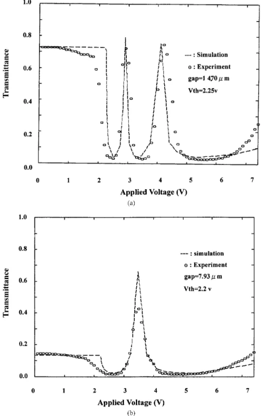
Plots of the voltage-dependent transmittance, including both theoretical calculation and experimental measured values corresponding to Figure 2, are given in Figure 3. The small discrepancy can come from the fact that the LC molecules close to the alignment surface do not reorient even though the applied voltage is sufficient. From this figure, it is conve-nient for us to estimate the cavity length of an LC᎐FPI filter as well as the FWHM of the filter, based on the
voltage-de-w x pendent equivalent refractive index by ERI analysis 6 . The cavity length is a basic parameter to evaluate the resonance
Ž .
wavelengths, and hence the free spectral range FSR and tunable range. It can be derived as
1 1
Ž .
ds ⭈ s ⭈ 1
Ž . Ž .
2 nr1y nr 2 2 n Vr1 y n Vr 2
where Vr1 and Vr 2 are the required voltage for two adjacent resonance peaks, which correspond to the required refractive indexes nr1 and n , respectively. Considering a sample withr 2
w Ž .x an LC cell spaced by the 15 m spacer Fig. 2 a , two adjacent peaks in the transmittance curve are present at Vr1s 2.9 V and V s 4.3 V, corresponding to n s 1.5281r 2 r1
Figure 2 Photographs of the experimental results on the depen-dence of the transmittance by ‘‘intensity measurement’’ which is shown on an oscilloscope with detector signals in the y-axis and
Ž . Ž .
tuning voltage in the x-axis. The LC cells have a 15m and b 8 m spacers
Figure 1 Setup for the ‘‘intensity measurement’’ experiment
Figure 3 Simulated and experimental results on the dependence of the transmittance by ‘‘intensity measurement’’ for different LC
Ž . Ž .
cells with a 15m, and b 8 m spacers
and nr 2s 1.5063, respectively. Thus, the cavity gap was
esti-mated to be 14.57m.
It is easily understood that the full voltage width at the half maximum in voltage-dependent transmittance character-istics corresponds to the full bandwidth at the half maximum in the wavelength-dependent transmittance characteristics. To obtain the FWHM of a passband centered at wavelength , the wavelengths at the half maximum of the transmittance0
and have to be measured. That is, a voltage V induces1 2 0
Ž .
an equivalent refractive index n0s nequV , in which the0
effective cavity gap for resonance is equal to n0⭈ L, such that
light at a wavelength passes through the LC᎐FPI filter at0
maximum. On the other hand, when V1 is applied, n1s
Ž .
nequV , where the effective cavity gap equals n1 1⭈ L, and
hence, only a half maximum of transmittance at would1
pass through the filter. The relationship between V and n2 2
at is similar to the case.2 1
The FWHM is mathematically expressed as FWHMs1
y , where and correspond to the refractive indexes2 1 2
n and n as well as the applied voltages V and V , respec-1 2 1 2
MICROWAVE AND OPTICAL TECHNOLOGY LETTERS / Vol. 22, No. 1, July 5 1999 50
tively. Thus, the FWHM becomes
Ž . Ž . Ž Ž . . Ž Ž . . Ž . FWHMs n y n s n V1 2 1 y n V2 2 where V and V can be obtained from the above measure-1 2
ment. We thus have
n2
Ž . Ž .
FWHMs y s 2 y s 21 2 2 0 0
ž
y 1/
3 n0Ž . Ž . Ž .
due to the fact that 2 n r s 2 n r s 2 n r0 0 1 1 2 2
s m at the same resonance order m.
w Ž .x
For the case of an 8 m spacer Fig. 2 b , we get V0s 3.62 V and V s 3.48 V, which give n s 1.5129 and2 0
n2s 1.5152, respectively. The variation of nequ with respect to the external electric voltage is on the order of magnitude of 10y3. Substituting these data into the above equation, we estimate the FWHM to be 1.92 nm; yet, that which was given by an optical spectrum analyzer is 1.96 nm. The accuracy of FWHM estimation is strongly influenced by both the stability of the externally applied voltage and the coupling ratio. Because the FWHM estimation focuses on the much smaller region calculation in the transmittance curve, it naturally requires a much more strict experimental condition.
4. CONCLUSIONS
A novel technique to characterize an electrically tunable LC᎐FPI was presented. Only the usual set of a monochro-matic light source and an optical power meter is needed. It is based on the equivalent-refractive-index analysis of a liquid-crystal Fabry᎐Perot etalon. Estimation of the cavity length and FWHM was achieved according to the measured voltage-dependent transmittance function.
REFERENCES
1. Y. Suzuki, N. Ohta, and K. Hirabayashi, Nonlinear distortion due to Fabry᎐Perot optical filter in direct modulated dense WDM-SCM viedo distribution systems, IEEE Photon Technol Lett 4 Ž1993 , 466. ᎐468.
2. K. Hirabayashi, H. Tsuda, and T. Kurokawa, Tunable liquid-crystal Fabry᎐Perot interferometer filter for wavelength-division
multi-Ž .
plexing communication systems, J Lightwave Technol 5 1993 , 2033᎐2043.
3. H. Tsuda, H. Uenohara, H. Iwamura, K. Hirabayashi, and T. Kurokawa, Tunable wavelength conversion using a liquid crystal
Ž .
filter and a bistable laser diode, Appl Phys Lett 61 1992 , 2006᎐2008.
4. M.W. Maeda, J.S. Patel, L. Chinlon, J. Horrobin, and R. Spicer, Electrically tunable liquid-crystal etalon filter for high-density
Ž .
WDM system, IEEE Photon Technol Lett 2 1990 , 820᎐822. 5. J.S. Patch, M.A. Saifi, D.W. Berreman, L. Chinlon, N.
An-dreadakis, and S.D. Lee, Electrically tunable optical filter for infrared wavelength using liquid crystal in a Fabry᎐Perot etalon,
Ž .
Appl Phys Lett 57 1990 , 1718᎐1719.
6. P.-L. Chen, K.-C. Lin, W.-C. Chuang, Y.-C. Tzent, K.-Y Lee, and W.-Y. Lee, Analysis of a liquid crystal Fabry᎐Perot etalon filter: A
Ž .
novel model, IEEE Photon Technol Lett 9 1997 , 467᎐469. 䊚 1999 John Wiley & Sons, Inc.
CCC 0895-2477r99
MILLIMETER-WAVE ARRAY FED
THROUGH THICK SLOTS FILLED
WITH DIELECTRIC
M. El Haj Sleimen,1M. Himdi,1J. P. Daniel,1N. Haese,2
and P. A. Rolland2
1UPRES-A CNRS 6075 Structure Rayonnantes/ Antennes et Reseaux ´ Universite de Rennes I´
35042 Rennes, France 2
Departement Hyperfrequences et Semiconducteurs´ ´ IEMN UMR CNRS 9929
59652 Villeneuve d’Ascq Cedex, France
Recei¨ed 5 January 1999
ABSTRACT: This paper deals with millimeter-wa¨e microstrip antenna arrays. The objecti¨es were to de¨elop and optimize a microstrip-to-thick-slot-line transition near 40 GHz, and to feed a printed array with this kind of transition. The influence of such a transition between the two
(
layers, and its effect on the radiation properties pattern symmetry, )
sidelobe le¨el ha¨e been checked. A study of the microstriprthick-slotr microstrip transition is first presented. Then, a comparison is made between radiated fields of arrays fed directly and through slot transitions. 䊚 1999 John Wiley & Sons, Inc. Microwave Opt Technol Lett 22: 51᎐53, 1999.
Key words: millimeter wa¨e; thick slot; transition; radiation patterns 1. INTRODUCTION
The development of civil applications in the millimeter-wave domain already requires the realization of antenna arrays in this frequency band. Microstrip technology is attractive at these frequencies if one uses materials with weak losses and cost.
But a problem often appears in the millimeter-wave do-main; spurious radiations, owing to the feeding network, occur. They are combined with the wanted radiation of the array which is degraded. These effects will affect the cross-polarization component and the sidelobe levels of the copo-larization component.
A means to palliate this problem is to print the array on two distinct faces: the radiating elements on one face, and the feeding network, responsible for the parasitic radiation, on the other. To join the two faces of the circuit, various options are foreseeable. Among them are the
microstrip-to-w x
coaxial transition 1 , and the microstrip-to-thick-slot transi-tion. The latter solution is chosen in this paper.
We will begin with a study of this transition. Then we will use it to feed a printed array, and will observe the effects of this association on the radio electrical behavior of the array.
2. MICROSTRIP-TO-THICK-SLOT TRANSITION IN MILLIMETER-WAVE DOMAIN
2.1. Description of the Transition. The structure is composed of a thick slot filled with dielectric that couples two
mi-Ž .
crostrip lines printed on different layers Fig. 1 .
The dielectric used here is a polymer, homogeneous, low-cost, and well suited for microwaves material: the
poly-w x
methyl᎐pentene alias TPX 2 . In the range of 39 GHz, its Ž .
thickness h equals 254m. It presents the following
dielec-Ž . y3
tric characteristics: s 2.1 and tan ␦ s 10 . The metal-r
Ž . ization is copper with 17.5m thickness t .
The thick support in which the slot is engraved is copper or other plated material of H thickness.s