Strong enhancement of the optical and electrical properties,
and spontaneous formation of an ordered superlattice
in
(111) B AlGaAs
Albert Chin a, * , H.Y. Lin a, K.Y. Hsieh b
a Department of Electronics Engineering, National Chiao Tung University, Hsinchy Taiwan, ROC b Institute of Materials Science and Engineering, National Sun Yet-Sen University, Kaohsiung, Taiwan, ROC
Abstract
Strong enhancement in the luminescence intensity is observed in Al,,,Ga,,,8As epitaxial layers grown on misoriented (111)B GaAs as compared to those simultaneously grown on (100) GaAs. For a 1” misorientation the luminescence intensity is almost 10 to 1000 times that of the (100) layers, depending on the growth temperature. Room temperature electron mobility for 3” misoriented (111)B Al o,leGa,,,As is 19% higher than that for side-by-side grown (100). The strong luminescence associated with a large red shift of 90 meV and the 19% mobility enhancement are related to the long range composition ordering in (111)B AlGaAs, which is observed by cross-sectional transmission electron microscopy in a 280 A Al,.,GaAs quantum well heterostructure with Al,,,GaAs barriers grown on (111)B GaAs substrates.
1. Introduction
Owing to the enhanced optical and electrical properties of improved quantum confinement and reduced alloy scattering, the spontaneous forma- tion of ordered ternary compound semiconduc- tors during growth has become a topic of increas- ing interest [l-4]. Most of these studies focused on GaInP [1,2] and InGaAs [3]; however, the growth of AlGaAs is particularly important for most opto-electronic and microwave devices ap- plications. Unfortunately, the quality of AlGaAs strongly depends on the growth conditions. Fur-
* Corresponding author.
thermore, a high growth temperature of 700°C is generally required for (100) AlGaAs in order to improve the optical quality. The difficulties of AlGaAs can be overcome if the AlGaAs material is spontaneously ordered and forms a quantum confined microstructure. Owing to the high sur- face migration velocity of adatoms on the (111)B surface [5], fundamental growth mechanisms can be improved and possible phase separation can be formed if AlGaAs is grown on this orientation.
Here we report the first observation of long- range composition ordering in (111)B AlGaAs. A one to three order of magnitude enhancement of integrated photoluminescence (PL) intensity, and a large red shift of 90 meV PL peak energy are also observed in Al,,z,Ga,,,,As grown on (111)B
OOZZ-0248/95/$09.50 0 1995 Elsevier Science B.V. All rights reserved SSDI 0022-0248(94)00858-2
A. Chin et al. /Journal of Crystal Growth 150 (1995) 436-440 437
when compared to those on (100). The measured RT electron mobilities for (111)B exceed the (100) mobility values by 19%, with similar carrier densi- ties.
2. Experimental procedure
Three sets of epitaxial structures were studied for optical, electrical, and structural characteriza- tion. For optical characterizations, PL was used to measure the optical properties of the undoped 2.0 pm thick Al,,,Ga,,,As layers. Four sub- strate temperatures, 600, 630, 650, and 670°C were chosen for layers grown on (100) and 1” misoriented (111)B. We also studied the degrees of misorientation effects on (111)B Al,,,Ga,,sAs. For electrical characterizations, a 0.3 pm Alc,,,Ga,,,As buffer layer and a 3.0 pm Si doped Alo,rsGa0,82As layer were grown at 630°C on (100) and misoriented (111)B GaAs substrates. Tem- perature dependent Hall measurement was used to characterize the electrical properties of the epitaxial layers and to analyze the scattering mechanism. For structure characterizations, cross-sectional transmission electron microscopy (TEM) was studied in a laser diode heterostruc- ture. The layer structure consists of 0.75 pm Si 06 Be doped Al,,Ga,,As barriers, and a 280 A undoped Al,,,Ga,,As quantum well (QW). The growth temperature was 600°C for the Al,,Ga,,As QW and 650°C for the Al,,Ga,,As barriers.
3. Results and discussion
Fig. 1 shows the PL spectra for AlGaAs grown at 630°C. A full width at half maximum (FWHM) linewidth of 4.4 meV for the (100) Al,,,Ga,,,As indicates the excellent quality of the AlGaAs layers. The (111)B AlGaAs layers show broad peaks without any resolvable fine structures. The peak energies decrease monotonically from 1.837 eV for (100) to 1.744 eV for the 3” (111)B layer. The 93 meV decrease of the PL peak energy resulting from the misorientation increase is re- lated to the monotonic increase of 30 times PL
1.0 .‘.,#“‘.““““’ 1
660 670 680 690 700 710 720
Wavelength
Fig. 1. Low temperature PL spectra of 2.0 Km thick Al,.,Ga,.,,As grown at 630°C on (100) and l”, 2”, and 3 misoriented (1ll)B GaAs.
integrated intensity. We believe that the PL is not due to impurity related transitions since the lay- ers have a low impurity content, and the 2.0 pm thick AlGaAs is totally depleted during Hall mea- surement.
Fig. 2 shows the PL spectra for the AlGaAs grown at 670°C. There is little PL integrated intensity enhancement and peak energy shift for 670°C grown samples, as compared to layers grown at 630°C. The integrated intensity en- hancement is about 1 to 4 times, while the peak energy shift is within 7 meV. The absence of any significant orientation dependence of the PL for
6.0 5.0 4.0 3.0 2.0 1.0 L 660 665 670 675 680 665 690 Wavelength
Fig. 2. Low temperature PL spectra of 2.0 pm thick A&,Ga,~,sAs grown at 670°C on (100) and l”, 2”, and 3” misoriented (111)B GaAs.
+ . 0 [IO01 n [11IlB . 0 . . 0 0 0 0 -I 580 600 620 640 660 680 700 720 Tempenture,°C
Fig. 3. Low temperature integrated PL intensity of mc.22Gaa.7s As grown by MBE on both WO) and (11l)B GaAs at different substrate temperatures.
the layers grown at 670°C is believed to be due to the high surface migration of both Al and Ga adatoms, which disorders the AlGaAs.
The dependence of the relative PL integrated intensity on growth temperature is shown in Fig. 3. A three orders of PL integrated intensity en- hancement for (111)B AlGaAs, grown at 600°C as compared to (100) AlGaAs, is very important to grow high optical quality AlGaAs at a low temperature of 600°C. The monotonic increase of PL integrated intensity with growth temperature on (100) AlGaAs is due to the reduction in the defect related non-radiative recombination cen- ters. This is expected from higher surface migra- tion velocities of adatoms and lower oxygen in- corporation at higher growth temperatures. In contrast, a decrease in the PL integrated intensi- ties for (111) AlGaAs as the growth temperature is increased cannot be explained by the above argument. It is believed to be due to the disorder- ing effect as growth temperature is increased.
The electrical properties of (111) AlGaAs were further evaluated by Hall measurements. The measured Hall data are summarized in Table 1. Both room temperature (RT) and 77 K electron
. . .
mobrlmes are hrgher for Ala,, Ga,,,As grown on (111) than that grown on (1001, and the mobility increases monotonically with the degree of mis- orientation. This is also consistent with the in- creased red shift of PL peak energy as degree of misorientation. Temperature dependent Hall mo-
Table I
Electrical characterization of Si-doped (100) and misoriented (111)B ~a,rsGaa,szAs Orienta- FRT P77K nRT n77K tion (cm2/ (cm2/ (cme3) (cm-“) V.s) V.s) 0” (100) 2200 2800 1.04 x 10’7 0.95 x 10’7 l”(111) 2260 2820 1.10x 1o17 0.94 x 1or7 2” (111) 2590 3140 0.98 x 10’7 0.95 x 10’7 3” (111) 2620 3220 1.00 x 10’7 0.94 x 10’7
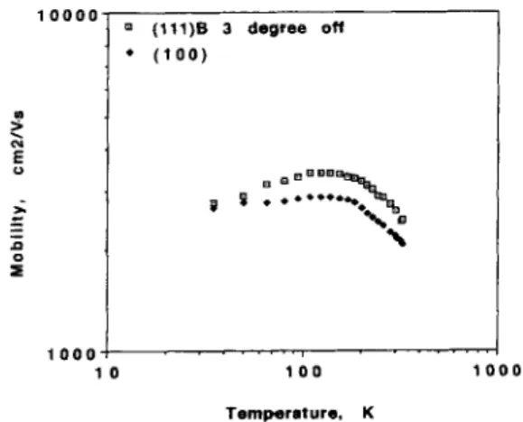
bility was also measured in order to probe the detailed scattering mechanisms. Fig. 4 shows the variation of Hall mobility with temperature in Si-doped (1001, and 3” misoriented (111)B Al- GaAs, respectively. The room temperature mobil- ity is primary limited by polar optical and space charge scattering, while the low temperature or 77 K mobilities are mainly limited by the ionized impurity scattering. However, these two mobility limiting mechanisms are related to both effective mass and Al composition. From the calculated and measured mobility data, the Al composition of (100) AlGaAs is determined to be 18%, which is consistent with the measured RHEED oscilla- tions data. However, for 3” misoriented (111)B AlGaAs, a good match between the total calcu- lated mobility and experimental data can be achieved only if the Al composition is adjusted to be 14%. This can be explained by the higher electron mobility of (111)B AlGaAs, compared to
1POOd
10 100 10’
Temperature, K
Fig. 4. Variation of Hall mobility with temperature in Si doped (100) and 3” misoriented (111)B A10,,sGa0,s2As.
A. Chin et al. /Journal of Crystal Growth 150 (1995) 436-440 439
0
7100
Wavelength(Angstrdm)
7600
Fig. 5. Low temperature PL spectra of Si doped (1001, 1” and 3” misoriented (111)B AlGaAs: (a) l”(lll)B; (b) 3Ylll)B; (c) (100).
the (100) case, at similar carrier concentrations. In order to justify the lower effective Al composi- tion in (111)B AlGaAs, we also measured PL of Si doped AIGaAs samples. Fig. 5 shows the mea- sured PL spectra, at 10 K, of Si-doped (loo), and 1” and 3” misoriented (111)B AlGaAs. The 46 meV red shift of the PL peak energy between (100) and 3” misoriented (111)B AlGaAs is equiv- alent to a 4% AI composition reduction, which is also consistent to the calculated Hall data.
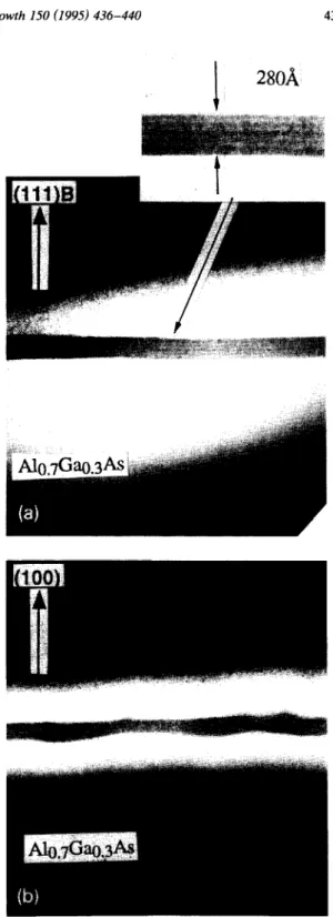
TEM was used to investigate the microstruc- ture of these samples and understand the red shift in PL peak energy. Figs. 6a and 6b show the cross-osectional (002) dark-field TEM images of a 280 A thick Al,,Ga,,,As/AI,,,Ga,,As single QW grown on (111)B and (100) GaAs, respec- tively. It is shown in Fig. 6b that the thickness of a QW heterostructure grown on (100) is rather non-uniform. This is expected from the relative low growth temperature of 650°C at the inverted A1,,Ga,,As/A1,,Ga,,As interface. However, for the QW grown on (lll)B, the well thickness is quite uniform and the inverted interface is very smooth. This is due to the much higher surface migration velocity of adatoms on (111)B than that on (100) orientation [5]. It is also noticed that there is a superstructure observed in the (111)B Al,,Ga,,As QW, which consists of a modulation of bright (AI-rich) and dark lines (Ga-rich) in the well region. These Al-rich and Ga-rich AlGaAs
Fig. 6. Cross-sectional view, dark field TEM image of 280 A thick Al,,,Ga,,,As quantum well for (a) (111)B and (b) (100) orientation. The AI,,Ga,~,As quantum well and Al,,,Ga,,As barrier were grown at 600 and 65O”C, respectively.
superlattice layers were parallel to the interface of the QW and were separated by approximately 55 A. In contrast, no such superstructure is ob- served in the side-by-side grown (100) QW. This result indicates that the superstructure is formed spontaneously during MBE growth, and is only formed on the (111)B orientation. To our best knowledge, this is the first reported long-range ordering, and spontaneous formation of Al-rich and Ga-rich Al,Ga, _,As/Al,Ga, _,As superlat- tice in AlGaAs. There is no such superstructure in the Al,,Ga,,As barrier due to the high growth temperature, which disorders the AlGaAs.
4. Conclusions
We have shown that a strong enhancement in the luminescence intensity of one to three orders can be obtained in misoriented (111)B Al,,,Ga,,+Ys epitaxial layers. The room temper- ature electron mobility for 3” misoriented (111)B AlO,,,Ga,,,,As is 19% higher than that for side- by-side grown (100). The strong luminescence as- sociated with a large red shift of 90 meV, and the 19% mobility enhancement are related to the
long range composition ordering in (111)B Al- GaAs, which is observed, by cross-sectional TEM, in a 280 A Al,,GaAs QW heterostructure with Al,,GaAs barriers, grown on (111)B GaAs sub- strates.
Acknowledgements
We would like to thank Dr. Z. Osman, U. Das, D.C. Liu and C.P. Lee for their help in PL measurements. The work has been supported by NSC (83-0404-E-009-097, and 83-0618-E-009-010) at Taiwan.
References
[l] K.Y. Cheng, K.C. Hsieh and J.N. Baillargeon, Appl. Phys. Lett. 60 (1992) 2892.
[2] K.C. Hsieh, J.N. Baillargeon and K.Y. Cheng, Appl. Phys. Lett. 57 (1990) 2244.
131 A. Chin T.Y. Chang, A. Ourmazd and E.M. Monberg, Appl. Phys. Lett. 58 (1991) 968.
[4] E.M. Stellini, K.Y. Cheng, P.J. Pearah, A.C. Chen, A.M. Moy and K.C. Hsieh, Appl. Phys. Lett. 62 (1993) 458. 151 Y. Nomura, Y. Morishita, S. Goto, Y. Katayama and T.