Abstract—In this paper, a novel ultra-low-power digitally
con-trolled oscillator (DCO) with cell-based design for system-on-chip (SoC) applications is presented. Based on the proposed segmental delay line (SDL) and hysteresis delay cell (HDC), the power con-sumption can be saved by 70% and 86.2% in coarse-tuning and fine-tuning stages, respectively, as compared with conventional approaches. Besides, the proposed DCO employs a cascade-stage structure to achieve high resolution and wide range at the same time. Measurement results show that power consumption of the proposed DCO can be improved to 140 W (@200 MHz) with 1.47-ps resolution. In addition, the proposed DCO can be imple-mented with standard cells, making it easily portable to different processes and very suitable for SoC applications.
Index Terms—All-digital phase-locked loop (ADPLL), cell-based
design, digitally controlled oscillator (DCO), hysteresis delay cell (HDC), portable, segmental delay line (SDL).
I. INTRODUCTION
P
HASE-LOCKED loop (PLL) is a very important clocking circuit for many electronic systems such as digital commu-nication and microprocessor. Traditional PLLs are designed by analog approaches. However, as supply voltage decreases, both gain and frequency range need to be traded off in voltage-con-trolled oscillator (VCO) which is the most important block in PLL. In addition, due to serious leakage current problem, it is hard to design a charge-pump circuit in more advanced process technology. Thus, it needs more design efforts to integrate analog PLLs in SoC with lower supply voltage and advanced process. Furthermore, as technology migrates, the analog blocks in PLL need to be re-designed. In contrast, all-digital phase-locked loop (ADPLL) [1]–[5] does not utilize any passive components and use digital design approaches, making it easily be integrated into digital and low-supply voltage systems.Basically, digitally controlled oscillator (DCO) dominates the major performances of ADPLL such as power consumption and jitter, and hence is the most important component of such clocking circuits [1]–[5]. Since DCO occupies over 50% power consumption of an ADPLL [2], the power consumption of DCO should be reduced further to save overall power dissipation to meet low-power demands in SoC designs. Recently, different architectural solutions have been proposed to implement the DCO. The current-starved type DCO [6] controls the supply
Manuscript received April 1, 2007; revised June 15, 2007. This work was sup-ported in part by the National Science Council of Taiwan, R.O.C., under Grant NSC-95-2220-E-009-291. This paper was recommended by Associate Editor A. Demosthenous.
The authors are with the Department of Electronics Engineering, National Chiao Tung University, Hsinchu 300, Taiwan, R.O.C. (e-mail: hysteria@ si2lab. org).
Digital Object Identifier 10.1109/TCSII.2007.903782
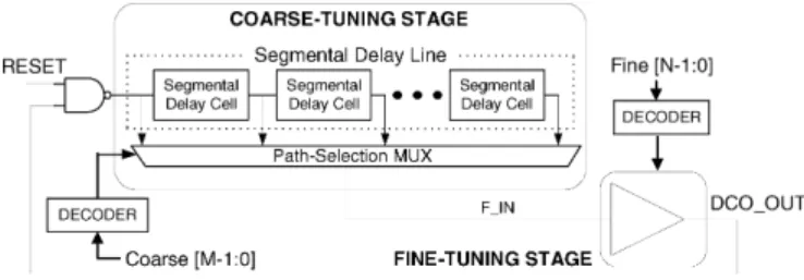
Fig. 1. Architecture of the proposed DCO.
current of delay cell to obtain different delay values. Although it has high resolution, it needs a static current source that will consume more static power dissipation. The LC tank DCO [7] can also achieve high delay resolution, however, it needs advanced process and requires intensive circuit layout. These approaches demand high complexity at circuit level, resulting in long design cycle and low portability.
In order to reduce design cycle when process or specification is changed, many DCOs implemented with standard cells have been proposed to enhance portability [2], [3], [8], [9]. Driving capability modulation (DCM) changes the driving current of each delay cell by controlling number of enabled tri-state buffers/inverters [2], [8]. The design concept of this approach is straightforward, but it has a poor performance in linearity and power consumption, and the resolution is insufficient. The or-and-inverter (OAI) cells are proposed to enhance resolution by different input pattern combinations; however linearity remains to be solved [3]. Although digitally controlled varactor (DCV) has a good performance in resolution and linearity [9], it is hard to take a few cells to provide wider operation range. As a result, large power consumption is demanded due to many DCV cells to maintain an acceptable operation range. Thus, this paper attempts to propose a low-power high-resolution wide-range DCO with high portability.
Fig. 1 illustrates the architecture of the proposed ultra-low-power DCO. Based on standard cells, our proposal can save power consumption and keep resolution. To preserve the con-trol code resolution and operation range, the proposed DCO employs cascading structure for both coarse-tuning and fine-tuning stages to maintain control code-to-delay linearity and ex-tend operation range easily. Two low-power circuit design tech-niques are proposed here. First, the proposed segmental delay line (SDL) can disable the transition of redundant segmental delay cells which is a two-inputANDgate in coarse-tuning stage at target operation frequency. Second, the hysteresis delay cell (HDC) is proposed for fine-tuning stage to reduce the number of short-delay cells.
Fig. 2. Proposed segmental coarse-tuning stage with SDL.
Fig. 3. Proposed fine-tuning stage with HDC and DCV.
II. PROPOSEDDCO ARCHITECTURE
A. Segmental Coarse-Tuning Stage
Fig. 2 shows the proposed segmental coarse-tuning stage, which is composed of two-inputANDgates that form a SDL and a path-selection multiplexer. It can provide dif-ferent delay values by selecting difdif-ferent delay paths organized by these two-inputANDgates. In the conventional delay line of path-selection schemes [3], [4], [9], the delay cell is com-posed of two inverters. When delay line is requested to provide higher operation frequency, a shorter delay path is selected and the rest delay cells will not be used. However, these delay cells are not disabled. To reduce power consumption as the operating frequency changes, some enabling input controlled signals (EN [ ]) are set to low level to disable those redundant two-inputANDgates, leading to save power consumption.
B. Fine-Tuning Stage
Because the resolution of the above mentioned coarse-tuning stage is not sufficient for typical DCO applications, a fine-tuning stage is added. In order to achieve better resolution and less power consumption, this fine-tuning stage is divided into three different substages as shown in Fig. 3. It should be noted that the controllable range of each stage is larger than the delay step of the previous stage. As a result, the cascading DCO struc-ture does not have any dead zone larger than the LSB resolu-tion of DCO. The delay steps of these fine-tuning substages are different; delay cells of the first stage and third stage have the largest and smallest delay step, respectively. Therefore, delay cell of the third fine-tuning stage determines the DCO LSB res-olution and controllable range of the first fine-tuning stage can cover the delay step of the coarse-tuning stage easily. Since the
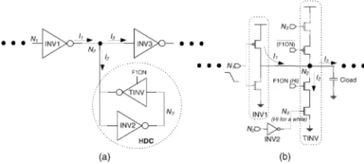
Fig. 4. (a) Proposed HDC. (b) Equivalent circuit of HDC for analysis.
proposed HDC can provide larger delay step than DCV, the first fine-tuning stage employs HDCs to replace many DCV cells, leading to save power consumption. Due to better resolution ca-pability, different DCVs are exploited in the second and third fine-tuning stages to improve the overall resolution of DCO. The operation concept of DCV is to control the gate capacitance of logic gate with input state to adjust the delay time [4], [9]. The second and third fine-tuning stages employ long-delay DCV cells (two-inputNAND) and short-delay DCV cells (tri-state inverter), respectively.
To optimize both power consumption and resolution, a strategy of allocating the proportion of the substages in the proposed fine-tuning stage is introduced. First, in order to achieve high operation frequency, should be limited to enlarge the length of total delay line in the fine-tuning stage. Then a suitable delay step of HDC can be determined by . Second, because the delay resolution is only determined by the delay step of DCV in the third fine-tuning stage, it needs to select a short-delay DCV from the cell library to meet the resolution requirement. After delay step has been determined, R can be chosen for the range of the third fine-tuning stage and the loading capacitance consideration. Finally, after the delay step adjustment of HDC and short-delay DCV, the delay step of long-delay DCV and in the second fine-tuning stage can also be determined. Note that Q can be reduced significantly by ex-ploiting HDC to save power. For example, if the requirement of output delay is 260 ps, it uses 4 HDCs to cover such delay range and 8 short-delay DCV cells to achieve high resolution. By the final step, 32 long-delay DCV cells are utilized to form the second fine-tuning stage. As a result, total power consumption and resolution of the proposed fine-tuning stage is 40.28 W and 0.97 ps, respectively, in a 0.13- m CMOS process.
C. Hysteresis Delay Cell
Fig. 4(a) illustrates the proposed HDCs used in the fine-tuning stage and each of which contains one inverter (INV2) and one tri-state inverter (TINV). As the input state of control signal
( ) of TINV in HDC changes,
dif-ferent delay of the third fine-tuning stage can be obtained. The operation concept of HDC is to control driving current to ob-tain different propagation delay. When TINV of the HDC is en-abled, the output signal of enabled TINV has the hysteresis phe-nomenon in the transition state to produce different delay times from the delay chain. Fig. 4(b) illustrates the equivalent circuit of HDC for analysis. The propagation delay from to
is a function of loading capacitance and equivalent resistance of turn-on MOS [10] and is given by
(1) where is the loading capacitance of , , and are equivalent resistance of NMOS and PMOS in the driving inverter (INV1), respectively. In the general operating situation, remains as a constant value. But, the equivalent resistance of turn-on MOS in INV1 varies with saturation current and drain-source voltage and is expressed by
(2)
where is the saturation current of transistor device. When TINV is enabled, since the input signal of TINV does not vary with the input of INV1 instantaneously, it will sink the inverse current to reduce the effective driving current from to .This leads to enlarge delay time of the delay chain. Fig. 5 shows the hysteresis phenomenon of this HDC, where input signal transition is observed from SPICE simulation. In the beginning, and remain at high level and is at low level. As signal level changes from high to low, the signal level of attempts to vary from low to high. However, because remains at high level for a while (delayed by INV2), TINV sinks the inverse current to slow down the pull-high speed of
. Thus, (2) should be rewritten as follows
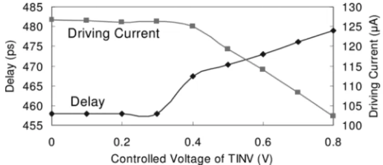
(3) The effective driving current changes from to
as TINV is enabled. The relation among input voltage of TINV, effective driving current, and INV1 delay is shown in Fig. 6. As the input voltage of TINV increases, the effec-tive driving current of INV1 will decrease, leading to enlarge the delay of inverter chain. In addition, based on the different driving capability tri-state inverters in a given cell library, a set of different delay steps of HDC can be constructed for a speci-fied DCO requirement.
III. DCO PERFORMANCECOMPARISONS
A. Coarse-Tuning Stage Performance Comparisons
For performance comparison, we rebuild those published ap-proaches with an in-house 0.13- m CMOS standard cell library
Fig. 6. Relation among input voltage of TINV, effective driving current, and INV1 delay.
Fig. 7. Power comparisons of different coarse-tuning designs.
and then compare with our proposal. Because the DCO con-sists of coarse and fine tuning stages in general, the performance comparisons are divided into two parts as well.
In the coarse-tuning stage, we reconstruct the conventional delay line of path-selection type by two-inverter delay cells for power consumption comparisons. For fair comparisons, both conventional and the proposed segmental coarse-tuning stages have the same operation range. In terms of different operation frequencies, the simulation results of power consumption are shown in Fig. 7. As compared with conventional approaches, the proposed segmental coarse-tuning stage can reduce 70% and 25% of the power consumption at 500 and 200 MHz, re-spectively. Because the number of disabled redundant delay cells varies with different operation frequencies; the segmental scheme has different power reduction ratio in different opera-tion frequencies.
B. Fine-Tuning Stage Performance Comparisons
The fine-tuning stage determines many major performance indexes of DCO, such as LSB resolution, delay linearity, and power consumption. Therefore, the performance comparisons of fine-tuning stage focus on these important performance in-dices. In the cell-based design approach, many designs exploit DCM or DCV to construct fine-tuning stage [2], [4], [8], [9]. For fair comparisons, these designs are rebuilt under the sim-ilar operation range and number of control bit. To ensure cor-rect functionality, the operation range of fine-tuning stage in all
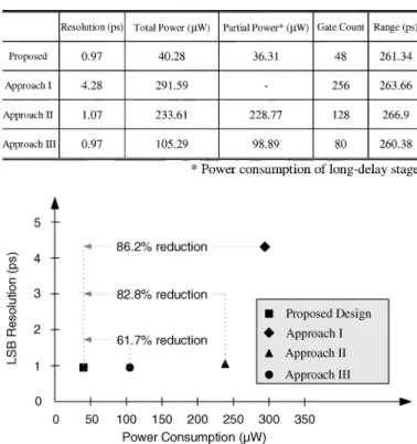
TABLE I
PERFORMANCECOMPARISONSWITHDIFFERENTFINE-TUNINGSTAGES
Fig. 8. Power and resolution comparisons of different fine-tuning designs.
comparison candidates should be larger than the minimum delay step of two-input AND gate, which is 200 ps in an in-house 0.13- m standard cell library. The rebuilt fine-tuning stages by different design approaches are: DCM type (Approach I) [2], [8], DCV type (Approach II) [9], and combination of DCM and DCV type (Approach III) [4]. The operation frequency range should be similar for fair comparisons, resulting in the different number of delay cells in different structures. For example, Ap-proach I, ApAp-proach II, and ApAp-proach III utilize 256, 128, and 80 tri-state inverters, respectively. In contrast to these approaches, the proposed structure only needs 12 tri-state inverters, 4 in-verters, and 32 two-input NAND gates (based on the strategy mentioned in Section II with and are assigned to 4, 32, and 8, respectively).
The performance comparisons simulated at 200 MHz at 0.8 V and typical corner cases, are summarized in Table I. Note that all of them have the similar performance in LSB resolution ex-cept Approach I. But, in terms of power consumption and area, the proposed design has significant improvement. Since the pro-posed HDC can replace many DCV cells to obtain wider op-eration range, the number of delay cells connected with each driving inverter and loading capacitance can be reduced, leading to save power consumption and gate count as well. The reduc-tion ratios are 86.2%, 82.8%, and 61.7%, as compared with Ap-proach I, ApAp-proach II, and ApAp-proach III, respectively. Fig. 8 also shows that our proposal has the high LSB resolution and low-power features as compared with the other designs.
Except Approach I, all of comparison candidates employ a short-delay DCV cell to form the finest delay cell; however, they utilize different type long-delay stages. Thus, we focus on the
Fig. 9. Microphotography and layout of DCO test chip.
TABLE II
MEASUREMENTRESULTS OFSTEP/RANGE OFTUNINGSTAGE
Fig. 10. Comparisons of measurement and post-layout simulation results.
power comparison of long-delay stage in different approaches. In contrast to Approach II whose long-delay stage only utilizes long-delay DCV cell, our proposal exploits HDC and hence has less long-delay DCV cells compared with Approach II. As a result, power-to-delay ratio of long-delay stage of our proposal and Approach II is 0.14 W ps (36.31 W/261.34 ps) and 0.86 W ps (228.77 W/266.9 ps), respectively. Based on this power comparison, it is clear that HDC-based structure can provide better power-to-delay ratio than pure DCV type structure, implying HDC is more effective in power saving for a given delay.
IV. IMPLEMENTATION ANDEXPERIMENTALRESULTS
Based on the requested frequency range and resolution for our application, the design parameters of the proposed DCO are
determined as follows: , , , ,
and . In order to verify the feasibility and performance of the proposed DCO in advanced processes, a test chip has been fabricated in 90-nm 1P9M CMOS process, where the chip mi-crophoto and layout of the DCO chip is shown in Fig. 9. The DCO output signal is measured using LeCroy SDA4000A at 1V/25 C (supply of I/O pad is 2.5 V) to test the performance. Due to the speed limitation of I/O pad, the DCO output fre-quency has to be divided by 2 when DCO operates at high frequency. Table II shows the delay step and operation range of different tuning stages in the proposed DCO. It shows that the controllable range of each stage is larger than the step of the previous stage, and the average DCO resolution is 1.47 ps. Fig. 10 shows the comparison between measurement results
Fig. 11. Jitter histogram of DCO at 952 MHz.
and post-layout simulation to illustrate the linearity analysis of the proposed DCO. Both root-mean-square (rms) and peak-to-peak phase jitter at 417 MHz is 8.18 and 49.05 ps, respectively. Fig. 11 shows the rms and peak-to-peak phase jitter is 8.24 and 49.95 ps, respectively, at 952 MHz under 1 V and 60 mV supply noise.
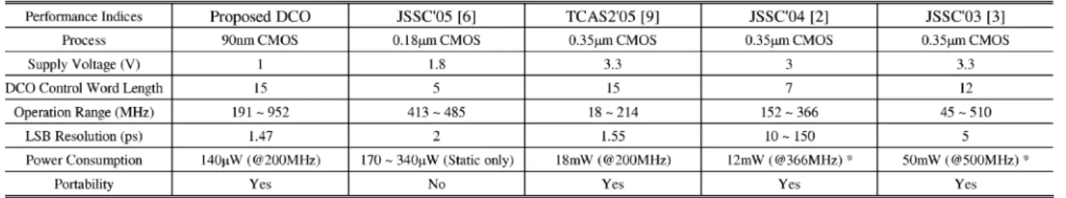
Table III lists comparison results with the state-of-the-art DCOs. In terms of power consumption, the proposed DCO has the lowest power consumption compared with other DCO de-signs. Furthermore, the proposed low-power solution does not induce any performance loss. Additionally, since the proposed DCO can be implemented with standard cells, it has a good portability. As a result the proposed DCO has the benefits of better resolution, operation range, linearity, and portability.
V. CONCLUSION
In this paper, we have proposed an ultra-low-power DCO with cell-based design for SoC applications. With the proposed seg-mental tuning structure and hysteriesis delay cell, the power consumption of coarse-tuning and fine-tuning stages can be fur-ther reduced by 70% and 86.2%, respectively, as compared with conventional designs. Measurement results show that our pro-posed DCO can achieve 1.47 ps resolution and 140 W at fre-quency of 200 MHz. As a result our proposal achieves not only
less power consumption, but also better LSB resolution and delay linearity of DCO. Moreover, because the proposed DCO has a good portability as a soft intellectual property (IP), it is very suitable for SoC applications as well as system-level integration.
ACKNOWLEDGMENT
The authors would like to thank their colleagues within the SI2 group of National Chiao Tung University, Taiwan, R.O.C., for many fruitful discussions in test chip design and implementation.
REFERENCES
[1] J. Dunning, G. Garcia, J. Lundberg, and E. Nuckolls, “An all-digital phase-locked loop with 50-cycle lock time suitable for high-perfor-mance microprocessors,” IEEE J. Solid-State Circuits, vol. 30, no. 4, pp. 412–422, Apr. 1995.
[2] T. Olsson and P. Nilsson, “A digitally controlled PLL for SoC applica-tions,” IEEE J. Solid-State Circuits, vol. 39, no. 5, pp. 751–760, May 2004.
[3] C.-C. Chung and C.-Y. Lee, “An all digital phase-locked loop for high-speed clock generation,” IEEE J. Solid-State Circuits, vol. 38, no. 2, pp. 347–351, Feb. 2003.
[4] D. Sheng, C.-C. Chung, and C.-Y. Lee, “An all-digital phase-locked loop with high-resolution for SoC applications,” in Proc. IEEE VLSI-DAT, Apr. 2006, pp. 207–210.
[5] R. B. Staszewski, D. Leipold, K. Muhammad, and P. T. Balsara, “All-digital PLL with ultra fast settling,” IEEE Trans. Circuits Syst. II, Exp. Briefs, vol. 54, no. 2, pp. 181–185, Jan. 2007.
[6] M. Maymandi-Nejad and M. Sachdev, “A monotonic digitally con-trolled delay element,” IEEE J. Solid-State Circuits, vol. 40, no. 11, pp. 2212–2219, Nov. 2005.
[7] R. B. Staszewski, D. Leipold, K. Muhammad, and P. T. Balsara, “Digitally controlled oscillator (DCO)-based architecture for RF frequency synthesis in a deep-submicrometer CMOS process,” IEEE Trans. Circuits Syst. II, Analog Digit. Signal Process., vol. 50, no. 11, pp. 815–828, Nov. 2003.
[8] E. Roth, M. Thalmann, N. Felber, and W. Fichtner, “A delay-line based DCO for multimedia applications using digital standard cells only,” in Proc. Dig. Tech. Papers ISSCC’03, Feb. 2003, pp. 432–433. [9] P.-L. Chen, C.-C. Chung, and C.-Y. Lee, “A portable digitally
con-trolled oscillator using novel varactors,” IEEE Trans. Circuits Syst. II, Exp. Briefs, vol. 52, no. 5, pp. 233–237, May 2005.
[10] J. M. Rabaey, Digital Integrated Circuits—A Design Perspective, second ed. Englewood Cliffs, NJ: Prentice-Hall, 2003.