Effects of Thermal N2 Annealing on Passivation Capabilily of
Sputtered Ta(-N) Layers Against Cu Oxidation
Jui-Chang Chuang and Moo-Chieh Chen
Departmentof Electronics Engineering and Institute of Electronics, National Chiao-Tung University, Hsinchu 300, Taiwan
ABSTRACT
The effects of thermal N3 annealing on the passivation capability of sputtered Ta and Ta-nitride [Ta(-N)] layers against Cu oxidation in a 200 A Ta(-N) covered Ta(-N)/Cu/Si02/Si structures was investigated. The N2 annealed Ta lay-ers revealed degradation in passivation capability, presumably due to grain growth of the Ta passivation layer. In con-trast, the nitrogen-doped Ta-nitride layers showed a contrary trend. For the Ta-nitride layer with 23.5 atom % of nitro-gen, passivation capability was effectively improved by N2 annealing at 300°C. For the Ta-nitride layer with 30.5 atom % of nitrogen, N2 annealing at higher temperatures (500—700°C) was necessary to improve the passivation capability. The healing of sputtering damage of Ta-nitride passivation layers by the thermal N2 annealing was responsible, presumably, for the improvement of passivation capability.
Introduction
Copperhas been extensively studied as a potential
sub-stitute for aluminum and Al alloys in multilevel metalliza-tion of semiconductor devices.'3 Compared with Al and Al alloys, Cu has a number of beneficial factors, such as lower bulk resistivity (1.7 vs. 2.7 and >4.0 mfl cm),"4 higher elec-tromigration resistance,5 higher melting point,4'5 and lower reactivity with commonly used diffusion barrier materi-als.6'7 However, there are obstructive factors compared with Al and Al alloys, such as difficulty in dry etching,8 poor adhesion to the dielectric layer,"2 easy diffusion in silicon and Si02,9'3 deep level trap in silicon, and Cu sili-cide formation at low temperatures. Thus, the use of bar-rier layers to reduce the diffusion of Cu and to improve its adhesion to dielectrics, especially Si02,8"42° is of great importance. The various barrier/adhesion layers for Cu metallization that have been extensively investigated are mostly listed in Ref. 14.
It is well known that Cu oxidizes easily in air and in humid ambient,21-24 even at room temperature. This char-acteristic has impeded the application of Cu in integrated circuits. A proper technique of passivation against Cu oxi-dation must be developed for its widespread application.25 So far; passivation schemes used to resist Cu oxidation in an oxidizing ambient have been studied"2 and proposed by some researchers, among them the self-aligned passivation by Al, Mg,24'27 Ti, Cr,28 and Nb,29 the sidewall passiva-tion30'3' by Mo and TiN, the formation of surface suicide,32 and the B-implanted Cu,33
Previously, the passivation capability of 200 A tantalum (Ta) and tantalum nitride (TaN or Ta2N) [or for short Ta(-N)] covered Cu films were studied and found by the authors to be able to withstand thermal annealing in flowing 03 at temperatures up to 400°C without Cu oxidation,34 In the current study, electrical measurement and various tech-niques of material analysis are used to study the effects of thermal N2 annealing of Th(-N)/Cu/Si02/Si structures on the passivation capability of Ta(-N) layers against Cu oxidation.
Experimenhl
For sample preparation, the starting materials were p-type, boron-doped, 3 in. diam Si wafers with nominal resis-tivity of 17-55 11 cm. After initial RCA cleaning, the Si wafers were thermally oxidized at 1050°C in steam to grow a 5000 A Si02. A Cu film 2000 A thick was sputter deposit-ed on the oxide layer; which was followdeposit-ed by a 200 A Ta or Ta-nitride film deposition on the Cu film in the same sput-tering system without breaking the vacuum. The Ta film was sputter deposited using a pure Ta target (99.999% purity) in Ar ambient, while the Ta-nitride films were deposited by reactive sputtering using the same Ta target in a gas mixture of Ar and N2 with various flow rates, The
* Electrochemical Society Active Member,
gases used were of electronic grade, and the base pressure of the deposition chamber was S X 10 Torr. All films were sputtered at a pressure of 7,8 mTorr without intentional substrate heating. Table I summarizes the sputtering con-dition and sample identification; the percentage atomic concentrations of nitrogen in the sputtered films are also tabulated.35
Then, the wafers were diced into 1.5 x 1.5 cm pieces for various thermal treatments. First, the diced wafers were thermally treated in N2 ambient for 30 mm at 300, 500, and 700°C separately; this thermal process is termed thermal N3 annealing. To study the effect of N2 annealing on the passivation capability, the as-deposited as well as the N2 annealed samples were thermally annealed in flowing 03 ambient for 50 mm at various temperatures. The sample identifications are summarized in Table II. A,3500, for example, is designated as sample A, thermally annealed in 02 ambient at 350°C without any N2 annealing, and B,N4500 is designated as sample B, annealed at 500°C in N2 ambient followed by thermal annealing in 02 ambient at 450°C.
Electrical measurement and material analysis were used to characterize the passivation capability of as-deposited and N2 annealed Ta and Ta-nitride films. Sheet resistance (Rs) was measured using a four-point probe. Scanning electron microscopy (SEM) was used to investigate surface morphology, X-ray photoelectron spectroscopy (XPS) was used for chemical state analysis, X-ray diffraction (XRD) analysis was used for phase identification, and secondary ion mass spectroscopy (SIMS) and Auger electron spec-troscopy (AES) were used for elemental depth profile analysis.
Resultsand Discussion
Thepassivation capability of 200 A Ta and Ta-nitride layers for the Ta(-N) covered Ta(-N)/Cu/Si03/Si structures in an oxidizing ambient was investigated in a previous study by the authors.34 It was also found that N3 annealing of these Ta(-N) layers did not change the chemical states and the atomic concentrations of tantalum and nitrogen.35 In the current study, the effects of N2 annealing on the pas-sivation capability of the Ta(-N) layers were examined.
TableI. Sputtering condition and nitrogen content of as-deposited Ta and Ta-nitride films.
A B C
Sample identification (Ta) (Ta-nitride) (Ta-nitride) Partial pressure of N2 in
sputtering gas (mTorr)
Deposition poweç(W)
Deposition rate (A/s)
0 150 0.3 1.52 150 0.3 2.4 150 0.3 Nitrogen atomic 0 23.5 30.5 concentration (%)
as-deposited N2 300°C annealing 500°C 700°C 350°C 02 400°C annealing 450°C 500°C A3N A2N A7N B3N B5N B?N 25 a. 20 15 •j 10
. 5
0 0. C3N C7N C33500 C5N3SOOC?N3500 C3N4000 C5N4000C7N4000 C3N4500 C5N4SOOC7N4SOO C3NS000 C7NS000C7N5000 IA2O0O
1 I I 2 3 4Cycle
(elemental) -932.75eVcYcle/\
A00
935 934 933 932 931 930Binding energy (eV)
A5N4000
Cycle
-(elemental) A 4000
932.75eV 5N Cu2p312:6
-(oxide) 933.3 eV cycle 0 I I I I I 935 934 933 932 931 930Binding energy (eV)
Table II. Summary of sample identification and N,/02 annealing temperatures.
A samples B samples C samples
A3500 A3N3SOO A2N3500 A?N3500 B3500 B3N3500 B5N3500 B7N3500 C3500 A4000 A3N4000 A5N4000 A?N4000 B,4000 B3N4000 B5N4000 B?N4000 C4000
A4500 A2N4SOO ASN4SOO A?N4500 Bas4500 B3N4SOO B5N4500 B?N4SOO C4500
A5000 A3NS000 ASNS000 A3N5000 B5000 B3N5000 BSN5000 B?N4SOO C5000
Ta Passivation Layers
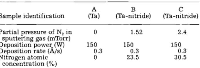
Asamples—Figure 1 shows the XRD spectra of 400°c 02 annealed A samples. Signals of the CuO phase appeared only in the spectrum of A7N4000 sample. Also, the sheet
resistance measured of this sample waseight times larger thanthat of the other samples, indicating the oxidation34 of Cu in this sample.
Figure 2 shows the SIMS depth profiles of A samples. There was not much structural difference between samples A4000 (Fig. 2a) and A5N4000 (Fig. 2 b). However, the
CuO(-111) CuO(-202) CuO(-311)
Cu(111)
A7N4000 ASN4000
AN4O0O samples showed a significant changein elemen-tal depth profiles (Fig. 2c), indicating the degradation of passivation capability resulting from a 700°CN2
anneal-ing.Figure 3 shows the XPS depth profiles of composi-tional elementsandthe binding energy spectra of Cu 2P3/2
photoelectrons for the Aas4000 and ASN4000 samples. A
A3N4000
A40OO
(a)
30 35 40 45
50 55 60
652
6 (degree)
Fig.1. XRD spectra of 400°C 02 annealed A samples.
0
v• Ta
5 6 7 I, a. U I, C 0 C 22 20 18 16 14 12 10 8 C(a)
C(b)
C(c)
1 0.0 0.1 0.2 0.3 0.4 0.5 0.6
DEPTH (sm)
ETa
108 1 o7 106i o
1 4 1 o 102 101 100 1 -1 -0 -t o 106 1 o 1 4 1 o3 102 101 100 I -1 -c 108io
106-iO
io
io
102 101 -100 10-1 -0.1(b)
12 C a.a 9
0I
0 a..1 0.0 0.1 0.20.3 0.4 0.5 0.6
DEPTH (nm)
C a. U C C 0 C 16 14 12 10 8 6 4 2 0.0 0.1 0.2 0.3 0.4 0.5 0.6DEPTH (nm)
Fig. 2. SIMS depth profiles of compositional elements for the samples (a) A,400O, (bi ASN4000, and (ci A7N4000.
Fig. 3. XPS depth profiles of compositional elements and XPS
binding energy spectra of Cu 2P3/2 photoelectrons for the samples (a) A0400O and (b) A5N4000.
J. Electrochem. Soc., Vol. 145, No. 11, November 1998 The Electrochemical Society, Inc. 4031
copperoxide phase of CuO was identified in the spectrum
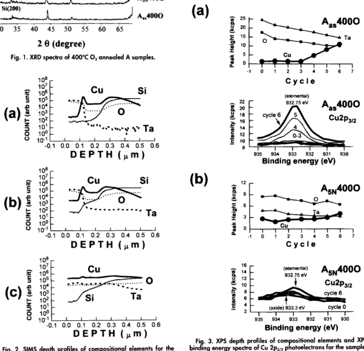
of ASN4000 (Fig. 3b, cycles 0) but not in the spectrum of A,400O (Fig. 3a). The degradation of passivation capabil-ity for the Ta passivation layer due to N2 annealing can be more clearly observed on the SEM micrographs shown in Fig. 4, in which CuO clusters224'36 are present on the sur-face of N2 annealed samples. The copper oxide phase of CuO was also determined by the XPS analysis for the sam-ple of A?N4000. In fact, the degradation occurred due to N2
annealing at temperatures as low as 300°C.
The degradation of passivation capability of Ta passiva-tion layer is presumably caused by the grain growth of the thin Ta passivation layer. Figures 5 and 6 show,
respec-tively, the XRD spectra and the surface morphology for A _________________________________________
30 35 40 45 50 55
60 65
2
0 (degree)
Fig.5. XRD specfra for A samples with and without N2 annealing.
samples with and without N2 annealing. The f3Ta signal
was detected on sample A7N (Fig. 5) and Ta flaking was observed on the surface of sample ASN as well as A7N (Fig. 6b). As the grain size became compatible with the film thickness, shorter diffusion paths'420'34' were built along the grain boundaries and the voids,34'35 leading to degradation of passivation capability.
Ta-NifridePassivation Layers
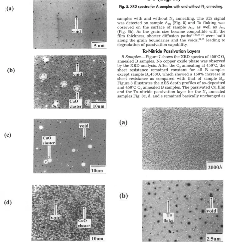
BSamples.—Figure 7 shows the XRDspectraof 450°C 02
annealed B samples. No copper oxide phase was observed by the XRD analysis. After the 02 annealing at 450°C, the sheet resistance remained constant for all B samples except sample B004500, which showed a 150% increase in sheet resistance as compared with that of sample Ba,. Figure 8 illustrates the AES depth profiles of as-deposited and 450°C 02 annealed B samples. The passivated Cu film and the Ta-nitride passivation layer for the N2 annealed samples Fig. 8c, d, and e remained basically unchanged as
$ Ta Si(200) Cu(111)
JjOL_J A
A
(a)
(b)
(a)
(c)
(b)
(d)
Fig. 4. SEM micrographs showing surface morphology for the Fig. 6. SEM micrographs showing surface morphology for the samples (a) A,,,4000, (b) A3N4000, (c) ASN4000, and (d) A7N4000. samples (a) A0, and (b) A7N.
CuO(-llt) CttO(200) j Cu(111)
B450O
B554500 B45OO B545OO30 35 40 45 50 55 60 65
Fig. 7. XRD specfra of 450°C °2 annealed B samples.
compared
with those of the as-deposited sample B0
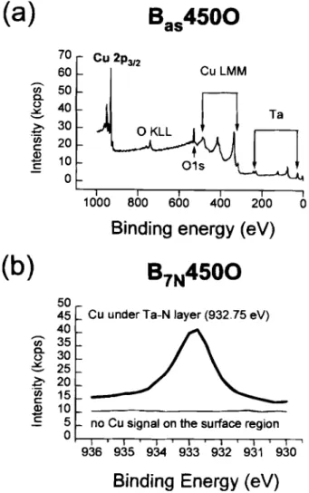
(Fig. 8a); however; complete intermixing of Cu, Ta, and 0 occurred for the sample of Bag4500 (Fig. 8b), which did not go through N2 annealing. Figure 9 shows the results of the XPS analysis. The Cu 2P212 photoelectrons were detected on the surface of sample B84500 (Fig. 9a), and were iden-tified to be in the state of CuO. The XPS spectra of Cu 2P3/2 photoelectrons for sample B?N4500 in the surface region and under the Ta-nitride layer are illustrated in Fig. 9b. No detectable Cu photoelectron was found in the surface region and the Ta-nitride layer. The Cu 2P3/2 photoelec-trons found under the Ta-nitride passivation layer were
determined to be in the elemental state. For sample
B7N4500, the only oxide phase detected by the XPS was Ta205 existing in the outermost surface region. Under the Ta205 layer; Ta 4f712 and N is photoelectrons remained in their nitride phase as were in the as-deposited sample!5
The N2 annealing process for B samples effectively improved the passivation capability of their passivation
lay-(d) ite B,,45OO Cu Cu p
:JF\1itq_
ATWA Nf
Ta/ V
V 4° P1 N -4 4 8 1812 14 14 2 Sputter Time (mln(Fig. 8. AESdepthprofiles of compositionalelementsfor the sam-pies (a) Be,, (b) B054500, (c) B3N4500, (d) BSN4500, and (e) BSN4SOO.
Bas4500
Cu 2p312 CuLMM TaOls
'JtLLJ
I I1000 800
600 400
200 0Binding energy (eV)
BTN4500
936 935 934 933 932 931 930
Binding Energy (eV)
Fig. 9. XPS specfra showing (a) surface compositional elements
survey for the sample B,,4500 and (b) binding energy spectrum of
Cu 2P3/2 photoelectrons for the sample B7N4SOO on the outermost surface as well as under the Ta-nifride passivation layer.
ers.And the superiority of passivation capability of sam-ple B0 over that of samsam-ple A5 was presumably due to amorphism2'3628 of the Ta-nitride layer. Figure 10 shows the surface morphology for the as-deposited Ta-nitride (or Ta2N)2° layer (Fig. iOa) as well as the 700°C N2 annealed film (Fig. iOb). No obvious grain growth of Ta-nitride was observed. This implies the fine grain of the Ta-nitride film and thus a long diffusion path for Cu along the grain boundaries. The thermal N2 annealing healed the micro-damage in the reactively sputtered Ta-nitride layer;25 how-ever; it resulted in new defects, i.e., void formation, as shown in Fig. Sb and lob. Thus, the passivation improve-ment was limited to thermal annealing in 02 ambient at 450°C. It was found that none of samples A or B, either with or without N2 annealing, can withstand a thermal annealing in 02 ambient at 500°C for 50 mm without the Cu film being oxidized.
C Samples—Figure ii shows the XRD spectra of 400°C 02 annealed C samples. Signals of the CuO phase were detected on sample Cas4000, which did not go through any N2 annealing process. For the sample annealed in N2 ambi-ent at 500°C, the signals of CuO diminished. For the sample annealed in N2 ambient at 700 and 800°C, a CuO phase sig-nal was not observed in the XRI)spectrum.Figure 12 shows
the percentage change of the sheet resistance resulting from thermal 02 annealing vs. temperatures of N2 annealing for C samples thermally annealed in 02 ambient at 350 and 400°C. The improvement of passivation capability resulting f mm
N2 annealing was indicated by the abrupt decrease of the sheet resistance change. For thermal 02 annealing at 350°C, N2 annealing at temperatures above 500°C was needed; for
70 60 50 40 30 20 10 0
2 0 (degree)
(a)
C/)a
0
>'
(I) C a, C(b)
Cu under Ta-N layer (932.75 eV) 50 45 40 c;;.. ssa. 0
-
25.' 20
1510
S 5
0 Bno Cu signal on the surface region
(a) its 80 548 Q C 44 28 2 45 810121415 IS
Spotter Time (minI
(b)
0 15 15 20 25 20 Sputter Time mini
(c)
gIeBI4UIu
2 4 4 8 10 12 14 ItSputter Time (mm)
(e)
'°°L1
0 4 t 8 IC 12 14 15the thermal 02 annealing at 400°C, N2 annealing at temper-atures above 700°C was needed. Figure 13 ifiustrates the AES depth profiles for C samples thermally annealed in 02 ambient at 350°C. For samples Cas3500andC5N3500, Cu was oxidized partially and the Ta-nitride passivation layer was covered with a layer of CuO (Fig. 13a and b). The extent of Cu oxidation was reduced by raising the N2 annealing temperature to 700°C (Fig. 13c). Figure 14 shows the SIMS depth profiles for C samples thermally annealed in 02 ambi-ent at 400°C. For sample C,4000, the original structure of Ta-nitride! Cu/Si02/Si was destroyed and copper oxide can be seen clearly (Fig. 14a). Similar results were observed for the samples with N2 annealing at temperatures below 700°C. For samples C?N4000 and C8N4000, which were annealed in N2 at 700 and 800°C, respectively, the original structure of Ta-nitride/Cu/Si02/Si retained its integrity (Fig. 14b and c). Figure 15 shows the XPS survey spectra of surface elements for the C samples. Only the samples annealed in N2 at 700°C did not reveal Cu 2p photoelectrons which were determined to be CuO phase. From the above
. Inn
Temperature of N2 pre-sinterlng (°C)
Fig. 12. Sheet resistance change (ARs/Rs) vs. temperature of N2
annealing for C samples thermally annealed in 02 ambient at 350
and 400°C.
Sputter Time (mm)
Fig. 13. AES depth profiles of compositional elements for the
samples (a) C0,3500, (b) C5N3500, and (c) C7N3500.
J. Electrochem. Soc., Vol. 145, No. 11, November 1998 The Electrochemical Society, Inc. 4033
600
+ 00
3500\
0
4000 0 i nn 200 400 600 800C350O
TaFig. 10. SEM micrographs showing surface morphology for the
samples (a, top) B0, and (b, bottom) B7N.
2 4 6
8 10 12 14 16
Sputter Time (mm) C5N 350 0(a)
100 80 60 C.)<40
20(b)
C.)4
(c)
100 8060
C.)4
40 20 20-S.
, 0
—2 4 6
8 10 12 14 16 Sputter Time (mm)Si(200)Cu(111)
Cu(200)J C4OOO
C7N 350 0J cooo
C54OOOCuO() C4OOO
30 35 40 45 50 55 60 65
2 0
(degree)
Fig.11. XRD spectra of 400°C 02 annealed C samples.
N
CuO
Cu
I I I0.0 0.1 0.2 0.3 0.4 0.5 0.6
DEPTH (1am)
0.0 0.1 0.2 0.3 0.4 0.5 0.6
DEPTH (nm)
I I 0.0 0.10.2 0.3 0.4 0.5 0.6
DEPTH (1am)
Fig. 14. SIMS depth profiles of compositional elements for the
samples (a) C0,4000, (b) C7N4000, and (c) CSN4000.
observation,we conclude that the passivation capability of C samples, can be improved by N2 annealing at tempera-tures above 700°C.
Figure 16 shows the XRD spectra of as-deposited and thermally N2 annealed C samples. A small peak belonging to the Ta-nitride phase appeared in the C?N spectrum. Similar to B samples, the thermal N2 annealing did not result in the change of atomic concentration and chemical state of Ta and N in C samples.35 A comparison of the sur-face morphologies of the as-deposited sample Ca. and the 700°C N2 annealed sample C?N is shown in Fig. 17. N2 annealing at 700°C resulted in no obvious grain growth. The amorphism of the Ta-nitride films of C samples is sim-ilar to that of B samples. However, the void formation (Fig. 17b) prohibited further improvement on the passivation capability by thermal N2 annealing at higher temperatures. To improve passivation capability, an N2 annealing at 300°C would be beneficial to sample B, but a 700°C N2 annealing was necessary for sample C to be effective. The differences lies in the degree of sputtering damage between sample Ba, and sample Cas. For the as-deposited sample Ca,, visible damage resulting from energetic N2 plasma during sputtering was observed (Fig. 17a). We presumed that the sputtering induced damage34'35 was responsible for the inferior passivation capability of sample Ca. as compared with sample Be,. The improvement of passivation capabil-ity for the high temperature N2 annealed C samples was principally due to sputtering damage healing.
Conclusion
Thiswork studied the effects of thermal N2 annealing on the passivation capability of sputtered Ta and Ta-nitride
C7N4000
C7N3500
Cu 2p Cu LMM Cu 3sC5N3500
Cu2p Ta 5sCas3500
1-I
P I 1000 800 600 400 200 0Binding Energy (eV)
Fig. 15. XPS survey spectra of surface compositional elements
for samples C,35OO, CSN3500, C7N3500, and C7N4000.
layersagainst Cu oxidation in a 200 A N) covered Ta(-N)/Cu/Si02/Si structure. For Ta passivation layers, the Ta/Cu/Si02/Si structure was able to sustain a thermal annealing in 02 ambient at 400°C for 50 mm without Cu oxidation. However N2 annealing at temperatures of 3 00°C and above resulted in the degradation of passivation
capability. This is, presumably, because thermal N2
annealing resulted in grain growth for the Ta passivation layer, leading to shorter paths of diffusion for Cu along the grain boundaries. The N-doped Ta-nitride layers revealed an opposite effect on passivation capability with respect to N2 annealing. For the Ta-nitride layer of sample B (with 23.5 atom % nitrogen in Ta-nitride), passivation capabili-ty was effectively improved by the N2 annealing process at 300°C. The N2 annealed sample was able to sustain ther-mal annealing in 02 ambient at temperatures up to 450°C without Cu oxidation. Moreover, the higher the N2 anneal-ing temperature was, the better the result of passivation became. For the Ta-nitride layer of sample C (with 30.5
Ta-N Si(2OO) Cu(111) -
.J C5
-- - - .— - —
-J ca
30 35 40
4550 55 60 65
2 0 (degree)
Fig. 16. XRD spectra of as-deposited and thermally N2 annealed C samples. 0 is Ta 4f N C .Q
(a)
C(b)
C(C)!
108io
106io
102 101 -100 10-1 -0.1 108 106 io5 i04 102 101 100 101 — -0.1io
io
106io
102 101 100 10-1 — -0.1 C.
I-. >1 9-U) C w 4-CSi
0
J. Electrochem. Soc., Vol. 145, No. 11, November 1998 The Electrochemical Society, Inc. 4035
atom % nitrogen in Ta-nitride), N2 annealing at higher temperatures of 500 to 700°C was needed for the improve-ment to be effective because the as-deposited Ta-nitride layer was more seriously damaged. The sputtering damage healing of Ta-nitride passivation layers of sample B and sample C by the thermal N2 annealing was, presumably, responsible for the improvement of passivation capability.
Acknowledgment
Theauthors wish to thank the Semiconductor Research Center of National Chiao-Tung University for providing an excellent processing environment. This work was sup-ported by the National Science Council, ROC, under con-tract NSC-86-22 1 5-E-009-040.
Manuscript submitted October 6, 1997; revised manu-script received August 14, 1998.
National Chiao-Tung University assisted in meeting the publication costs of this article.
REFERENCES
1. See, for example, MRS Bull., 18 (1993) and 19 (1994), devoted to the topic of copper metaffization for micro-electronics.
2. See, for example, Thin Solid Films, 262 (1995), devot-ed to copper-basdevot-ed metallization and interconnects for ultralarge-scale integration applications. 3. K. P. Rodbell, E. G. Colgan, and C.-K. Hu, Mater. Res.
Soc. Symp. Proc., 337, 59 (1994).
4. CRC Handbook of Chemistry and Physics, 73rd ed., D. R. Lide, Editor, Section 12, CRC Press, Inc., Boca Raton, FL (1992).
5. 5. Shingubara, K. Fujiki, A. Sano, H. Sakaue, and Y.
Horiike, Mater. Res. Soc. Symp. Proc., 338, p. 441, P. Børgesen, J. C. Coburn, J. E. Sanchez, Jr., K. P. Rod-bell, and W. F. Filter, Editors, Materials Research Society, Pittsburgh, PA (1994).
6. Binary Alloy Phase Diagrams, 2nd ed. T. B. Massalski, Editor, pp. 1446, 1485, 2703, and 2919, ASM Interna-tional, Material Park, OH (1990).
7. E. A. Brandes, Smithells Metals Handbook, 6th ed., Chap. 8, p. 21, Robert Hartnoll Ltd., Bodmin, Corn-wall, England (1983).
8. Y. Igarashi, T. Yamanobe, and T. Ito, Thin Solid Films,
262, 124 (1995).
9. J. D. McBrayer, R. M. Swanson, and T. W. Sigmon, J. Electrochem. Soc., 133, 1242 (1986).
10. Y. Shacham-Diamand, A. Dedhia, D. Hoffstetter, and W. G. Oldham, J. Elect rochem. Soc., 140, 2427 (1993). 11. D. Gupta, Mater. Res. Soc. Symp. Proc., 337, p. 209
(1994), 5. P. Murarka, A. Katz, K. N. Tu, and K. Maex, Editors, p. 209, Materials Research Society, Pittsburgh, PA (1994).
12. G. Raghaven, C. Chiang, P. B. Anders, S. M. Tzeng, R. Villasol, G. Bai, M. Bohr, and D. B. Fraser, Thin Solid Films, 262, 168 (1995).
13. S. M. Sze,Physicsof Semiconductor Devices, 2nd ed., Chap. 6-8, John Wiley & Sons, New York (1981). 14. 5. Q.Wang,S. Suthar C. Hoeflich, and B. J. Burrow, J.
Appi. Phys., 73, 2301 (1993).
15. J-C. Chiou, K-C. Juang, and M-C. Chen, J. Elec-trochem. Soc., 142, 2326 (1995).
16. J. S. Reid, E. Kolawa, R. P. Ruiz, and M-A. Nicolet, Thin Solid Films, 236, 319 (1993).
17. H. Ono, T. Nakano, and T. Ohta, Appl. Phys. Lett., 64, 1511 (1994).
18. K.-C. Park and K-B. Kim, J. Electrochem. Soc., 142, 3110 (1995).
19. J. 0. Olowolafe, J. Li, J. W. Mayer, and E. G. Colgan, Appi. Phys. Lett., 58, 469 (1991).
20. A. Noya, M. Takeyama, K. Sasaki, E. Aoyagi, and K. Hiraga, Jpn. J. Appl. Phys., Part 1, 33, 1528 (1994). 21. J. Li, J. W. Mayer, and E. G. Colgan, J. Appl. Phys., 70,
2820 (1991).
22. M. O'Reilly, X. Jiang, J. T. Beechinor, S. Lynch, C. NI Dheasuna, J. C. Patterson, and G. M. Crean, Appl. Surf. Sci., 91, 152 (1995).
23. H. K. Liou, J. S. Huang, and K. N. Th, J. AppI. Phys., 77, 5443 (1995).
24. A. J. Griffin, Jr., S. E. Hernández, and F. K. Brotzen, J. Electrochem. Soc., 141, 807 (1994).
25. C-K. Hu, B. Luther, F. B. Kaufman, J. Hummel, C. Uzoh, and D. J. Pearson, Thin Solid Films, 262, 84 (1995).
26. W. A. Lanford, P. J. Ding, W. Wang, S. Hymes, and S. P. Murarka, Thin Solid Films, 262, 234 (1995).
27. P. J. Ding, W. Wang, W. A. Lanford, S. Hymes, and S. P. Murarka, Appi. Phys. Lett., 65, 1778 (1994).
28. J. Li, J. W. Mayer, Y. Shacham-Diamond, and E. G. Col-gan, Appl. Phys. Lett., 60, 2983 (1992).
29. H. Itow, Y. Nakasaki, G. Minamihaba, K. Suguro, and H. Okano, AppI. Phys. Lett., 63, 934 (1993).
30. D. S. Gardner, J. Onuki, K. Kudoo, Y. Misawa, and Q.T. Vu, Thin Solid Films, 262, 104 (1995).
31. Y. Igarashi, T. Yamanobe, T. Yamaji, S. Nishikawa, and T. Ito, Jpn. J. Appl. Phys., Part 1, 33, 462 (1994). 32. 5. Hymes, S. P. Murarka, C. Shepard, and W. A.
Lan-ford, J. Appl. Phys., 71, 4623 (1992).
33. P. J. Ding, W. A. Lanford, S. Hymes, and S. P. Murarka, J. Appl. Phys., 74, 1331 (1993).
34. J-C Chuang and M-C. Chen, J. Electrochem. Soc., 145,
3170 (1998).
35. J-C Chuang and M-C. Chen, Thin Solid Films, 322, 213
(1998).
36. D. D. Wu, Masters Thesis, National Chiao-Thng Uni-versity, Hsinchu, Taiwan (1996).
37. Metallization in Silicon Processing for the VLSI Era, Vol. 1, S. Wolf and R. N. Tauber, Editors, Lattice Press, Sunset Beach, CA (1986).
38. K. Holloway, P. M. Fryer, C. Cabral, Jr., J. M. E. Harp-er, P. J. Bailey, and K. H. KellehHarp-er, J. Appl. Phys., 71, 5433 (1992).
Fig. 17. SEM micrographs showing surface morphology for the