The Growth and Raman Spectra of boron-doped Silicon Nanowires
Chao-Yu Meng, Jui-Lin Chen and Si-Chen Lee
Graduate Institute of Electronics Engineering and Department of Electrical Engineering,
National Taiwan University, Taipei, 106, Taiwan
Abstract — Boron-doped silicon nanowires, synthesized
under different temperatures and pressures, have been analysed by scanning electron microscope. The pressure affects the diameters of silicon nanowires more seriously than the temperature especially when growth temperature is below 440oC. The Fano fitting results of Raman spectra and the intensity ratio of anti-Stock / Stock reveal that the Raman downshift of boron-doped silicon nanowires is smaller than the un-doped ones due to the interaction between dopants and light induced plasma.
Index Terms — Raman spectrum, boron-doped, silicon
nanowires.
I. INTRODUCTION
In the last few years, nanomaterials have attracted increasing attention due to its quantum size effects and technological interest. Silicon nanowires (SiNWs) in particular are one of the most attractive materials because the existing semiconductor fabrication technologies are mainly based on Si. So it is important to investigate the growth parameters of SiNWs sufficiently and build up the onward nanowires technology based on them. To study the quantum confinement effect further, Raman spectroscopy is adopted due to its nondestructive nature. Various works on Raman spectra of undoped SiNWs have been reported recently [1-6]. The sample heating effects stemming from laser irradiation might be the dominant reason which causes the downshift and broadening of SiNWs Raman spectra [7]. Besides, the Fano effects should be also taken into account to characterize the asymmetric line shape.
In this paper, the boron doped SiNWs are studied using Raman spectra.
II. EXPERIMENT
Corning 1737F glasses were used as the template in this study. 20 nm Au colloids were sprayed onto the glass surface and served as the catalyst during Vapor-Liquid-Solid (VLS) growth. The flow ratio of B2H6 to SiH4 is
100ppm during the experiments. The process temperature and pressure varied from 430 to 460oC and from 5 to 25
torr, respectively. For comparison, the un-doped SiNWs
grown at 460oC were measured as the reference. The
variation of SiNWs diameters were measured by LEO 1530 high resolution SEM. Raman spectra was taken by Jobin Yvon T64000 system and Coherent Verdi-V10 532 nm laser.
III. RESULTS AND DISCUSSION
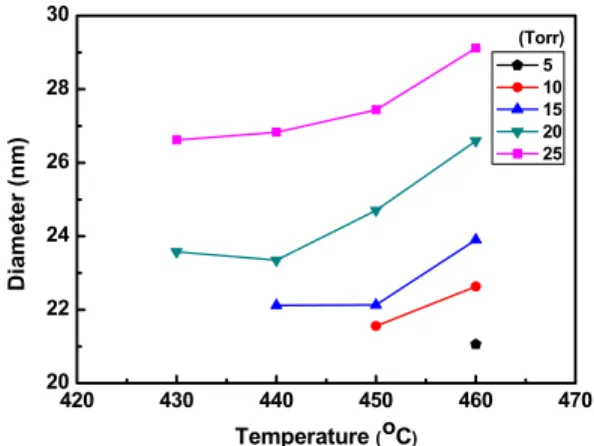
Fig. 1 illustrates the diameter variation of SiNWs under the different growth temperature. The growth pressure was an independent parameter. The diameter of SiNWs increases with the temperature. When the process pressure decreases the temperature needed to start the VLS process also increases. For examples, the temperature needed for the VLS growth at 5 Torr is higher than 460oC but it is
only 430oC at 20 torr.
Fig. 1. Diameter of SiNWs grown on 20 nm Au particles at different growth temperature.
The effect of pressure on the SiNWs growth on 20 nm Au particles is shown in Fig. 2. Comparing with temperature effect, it is much easier to control the SiNW diameter by the growth pressure. It is notable that the 430oC and 440oC curves of Fig. 2 overlaps. This means
that once the process temperature is below 440oC, the
diameter of the SiNWs becomes mainly dependent on the growth pressure. The 3D map showing the diameter of the SiNWs as a function of the process pressure and
420 430 440 450 460 470 20 22 24 26 28 30 Dia m et er (nm) Temperature (oC) 5 10 15 20 25 (Torr)
Proceedings of 2005 5th IEEE Conference on Nanotechnology Nagoya, Japan, July 2005
temperature is illustrated in Fig. 3. The intersection of the 3D surface and x-y plane is the lower limit to start VLS growth on 20 nm Au nanoparticles.
Fig. 2. Diameter of SiNWs at different growth pressure.
Fig. 3. Diameter mapping with respect to process pressure and temperature.
It should be noted that most parts of the SiNWs in our thin film are not contacted with the substrate but suspend by other nanowires thus leads to bad thermal contact with the substrate. Therefore, the heating effect of SiNWs with incident laser power will become more seriously than that of the silicon bulk substrate. Since the sample heating will cause the downshift of Raman spectra, the intensity ratio of anti-Stock/Stock (IAS/IS) becomes an important index to
identify the sample temperature. The IAS/IS ratio of
un-doped and boron-un-doped SiNWs grown at 460oC versus
laser power is shown in Fig. 4. The similar behaviors of these two curves illustrate the same heating effect. For the closed curves also reveal that the temperature of un-doped SiNWs is only slightly higher than the boron-doped one.
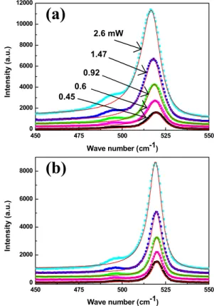
Figures 5 (a) and (b) show the Stokes Raman spectra of un-doped and boron-doped SiNWs, respectively. The
Fig. 4. Intensity ratio of anti-Stock/Stock (IAS/IS) as a
function of incident laser power.
scales of laser power used to measure the Raman spectra are kept the same for un-doped and boron-doped SiNWs. As the laser power increases the Raman line shape downshifts and asymmetrically broadens. Compared Fig. 5 (a) with Fig. 5 (b), it is found that the FWHM of un-doped SiNWs is much more broaden than those of the boron-doped SiNWs. It means the phonon life time in un-doped SiNWs is shorter than that in the boron-un-doped ones.
Fig. 5. Stokes Raman spectra of (a) un-doped and (b) boron-doped SiNWs versus differenct incident laser power. The solids line represent the fits of Fano resonance line shape. 5 10 15 20 25 20 22 24 26 28 30 (oC) Diam et er ( n m) Pressure (torr) 430 440 450 460 460 455 450 445 440 435 430 22 24 26 28 30 5 10 15 20 25 D ia m et er ( nm ) Pressu re (to rr) Tem pera ture(o C) 21 22 23 24 25 26 27 28 29 30 (nm) 450 475 500 525 550 0 2000 4000 6000 8000 10000 12000 Inte ns ity (a .u. ) Wave number (cm-1) 450 475 500 525 550 0 2000 4000 6000 8000 Inte ns ity (a .u.) Wave number (cm-1)
(a)
(b)
0.45 0.6 0.92 1.47 2.6 mW 0.14 0.16 0.18 0.20 0.22 I AS /IS P IThe solid lines represent the fits of the Raman spectra to a Fano resonance line shape given by[8]
(1)
where ωο is the renormalized phonon frequency in the
presence of coupled scattering, q is the asymmetry parameter (q → ∞ gives a Lorentzian), and Γis the line-width parameter. Fano interference scattering in doped bulk silicon has been extensively dealt with in earlier Raman studies [9-13]. The interference scattering results in an asymmetry line shape as described by Eq. (1).
Fig. 6. Parameters extracted by fitting the Fano resonance line shape versus incident laser power. ((a) peak positionωο, (b) line width Γ, and (c) asymmetry factor |1/q| )
With sufficiently high doping levels, electrons or holes will take part in the light-scattering process and excite the free carriers to the next higher conduction band or valance band. And the electronic continuum cooperated with LO (TO) phonons results in the asymmetric Fano line shape.
The Fano parameters extracted from the fitting curves in Fig. 5 are plotted in Figs. 6 (a) ~ (c) versus incident laser power. Compared Fig. 6 (a) with Fig. 4, it is found that when the incident laser power is below 0.45 mW the temperature of these samples is around room temperature and the difference of Raman downshift between un-doped and boron-doped SiNWs is only 0.1 cm-1. As the incident
laser power increases, the downshift of un-doped SiNWs increases rapidly but that of the boron-doped SiNWs changes only slightly. The causes of the Raman peak downshift can be describes as follows: (I) The temperature effects, (II) the stress effects, (III) the effects of high carrier densities. Since the temperature of un-doped and boron-doped SiNWs is close from Fig. 4 and there isn’t additional stress applied on these samples thus the main reason of the different downshift must stem from the doping effects. This result also corresponds to the variation of 1/q factor which has been found proportional to the free carrier concentration in bulk silicon [9-10]. With the increment of incident laser power, the injected free carriers also increase and participate in the light-scattering process as described above.
For the heavily doped p-type bulk silicon, the doping concentration needed to achieve a 2 cm-1 shift is about 1×
1020 cm-3 [13] but in our case the concentration calculated
from the mole fraction ratio is only about 1×1019 cm-3
which is one order below the concentration needed in bulk silicon. This fact reveals that the doping or injected free carriers induced electronic continuum interference, which cooperated with the LO (TO) phonon, affects the downshift of Raman peak more seriously than in bulk silicon.
IV. CONCLUSION
Boron-doped silicon nanowires, synthesized under different temperatures and pressures, have been analysed. The pressure affects the diameters of silicon nanowires more seriously than the temperature especially when growth temperature is below 440oC. And the lower limit
of the SiNWs growth as a function of the process pressure and temperature is also found.
Suspended SiNWs are more easily to be heated by incident laser than bulk silicon due to poor thermal contact with the substrate. Since sample heating plays an important role when doing Raman spectra measurement. Therefore, the intensity ratio of anti-Stock/Stock (IAS/IS)
( )
(
(
2)
)
21
ε
ε
ω
+
+
=
A
q
I
(
)
Γ
−
=
ω
ω
οε
0 1 2 3 0.02 0.04 0.06 0.08 0.10 0.12 |1/ q | Laser Power (mW) p i 517 518 519 520 521 ωο ( cm -1 ) p i 3 4 5 6 7 Γ ( cm -1) p i(a)
(b)
(c)
becomes an important index to identify the sample temperature. Besides, unlike the bulk silicon, the doping or injected free carriers affects the downshift of Raman peak more seriously than in bulk silicon.
REFERENCES
[1] B. Li et al., “Raman spectral study of silicon nanowires” Phys. Rev. B 59, 1645 (1999)
[2] R. P. Wang et al., “Raman spectral study of silicon nanowires: High-order scattering and phonon confinement effects” Phys. Rev. B 61, 16827 (2000)
[3] S.L. Zhang et al., “Variation of Raman feature on excitation wavelength in silicon nanowires” Appl. Phys. Lett. 81, 4446 (2002)
[4] D. P. Yu et al., “Nanoscale silicon wires synthesized using simple physical evaporation” Appl. Phys. Lett. 72, 3458 (1998)
[5] S. Hofmann et al., “Gold catalyzed growth of silicon nanowires by plasma enhanced chemical vapor deposition.pdf “ J. Appl. Phys. 94, 6005 (2003)
[6] R. Gupta et al., “Laser-Induced Fano Resonance Scattering in Silicon Nanowires” Nano Lett. 3, 627 (2003)
[7] S. Piscanec et al., “Raman spectroscopy of silicon nanowires” Phys. Rev. B 68, 241312 (2003)
[8] U.Fano, “Effects of Configuration Interaction on Intensities and Phase Shifts” Phys. Rev. 124, 1866 (1961)
[9] M. Balkanski et al., “Theory of interference distortion of Raman scattering line shapes in semiconductors” Phys. Rev. B 12, 4328 (1975)
[10]F. Cerdeira et al., “Effects of carrier concentration on the Raman frequencies of Si and Ge” Phys. Rev. B 5, 1440 (1972)
[11]M. Chandrasekhar et al., “Effects of interband excitations on Raman phonons in heavily doped n-Si” Phys. Rev. B 17, 1623 (1978)
[12]N. H. Nickel et al., “Raman spectroscopy of heavily doped polycrystalline silicon thin films” Phys. Rev. B 61, 15558 (2000)
[13]R. Beserman et al., “Raman scattering measurement of the free-carrier concentration and of the impurity location in boron-implanted silicon” J. Appl. Phys. 48, 1548 (1977)