Characterization of Asymmetrical Half Bridge Flyback Converter
Tso-Min Chen,
Student Member,
IEEE
and Chern-Lin Chen,
Senior Member,
IEEE
Graduate Institute of Electronics Engineering & Department of Electrical EngineeringNational Taiwan University Taipei, Taiwan 106
Abstract
-
Flyback derived converters are attractive because of their simple capacitive output fdter when compared with other converters used in multiple-output or cost-sensitive applications. This paper analyzes the detailed circuit behavior of the asymmetrical half bridge flyback converter. Several practical issues, including the specific relationships between the duty cycle and the different types of energy in the energy-storage elements, and the zero voltage switching (ZVS) conditions of the power switches have been thoroughly examined. Mathematical equations have also been given. A 5Vl20A prototype has been built to verify the analytical results.I. INTRODUCTION
The conventional flyback converter is attractive where multiple-output or cost-sensitive applications are concerned, thanks to its simple capacitive output filter. Nevertheless, hard switching operation of the power switch results in high switching loss, high EMI noises, and high switch voltage stress. Various kinds of soft switching techniques have been proposed for flyback converters [l-81. Among them, the resonant converter [l-21, the active-clamp circuit [3-51, and the asymmetrical half bridge converter are probably the most well known converters. Resonant converter can reduce the switching losses and EM1 noises. However, the voltage andor current stresses increase and result in high conduction losses. Incorporation of active clamp network provides the benefit of ZVS operation of the power switches in the active clamp flyback converter [3-51. However, the drawback that we will have to bear is the high voltage stresses on the power switches.
The asymmetrical half bridge flyback converter, which can achieve ZVS operations of the power switches, is gaining popularity. The switch voltage stresses are no more than the input voltage can be achieved. In the previous works [6-81, the role of the blocking capacitor in the process of energy storing has been overlooked. When only the magnetic components are being considered as the energy-storage elements in the studied converter, a 50% duty cycle constraint has been derived [8]. However, in the present paper, it has been proved that the 50% duty cycle constraint does not occur. This is because the blocking capacitor also stores energy when the output rectifier is off. The specific relationships between the duty cycle and the various types of energy in the energy-storage elements have been examined in depth.
This work was supported partially under the contract NSC 90-22 13-E-002-120 by National Science Council, Taiwan.
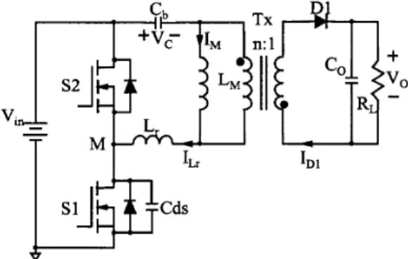
Fig. 1 shows the simplified circuit diagram of the asymmetrical half bridge flyback converter. The ZVS conditions for the power switches, SI and S2, have not yet been discussed before. In fact, the ZVS mechanisms of them are quite different. One of them is just a linear charging process. The ZVS operation of this power switch, S2, can be maintained simply when there is a sufficiently long dead time between SI and S2. However, the ZVS operation of the other switch, S I , is achieved only when the energy stored in the resonant inductor is greater than that of the output capacitors of these power switches.
A 5Vl20A prototype has been built to verify the analytical results. With the assistance of the given design equations, the power switches can maintain ZVS from no-load to full-load situations.
11. STEADY-STATE OPERATION
Fig. 1 shows the simplified circuit diagram of the asymmetrical half bridge flyback converter. The inductor L, denotes the combination of the leakage inductance of Tx
and the external inductor. To describe the basic operational principles, several assumptions are made.
The converter has reached a steady-state operation. L, is much less than LM.
The resonant period of Cband L, is much greater than the off time of S I .
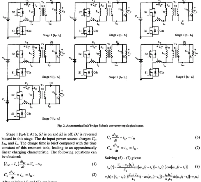
To facilitate the analysis of the asymmetrical half bridge flyback converter, Fig. 2 and Fig. 3 show the seven topological stages of the converter during a switching cycle and its key waveforms, respectively. The operations of this converter can be explained as follows:
Fig. 1. Simplified schematic of the asymmetrical half bridge flyback Converter.
PCds
Stage 7 [k- to1Fig. 2. Asymmetrical half bridge flyback converter topological states. Stage 1 [b-t,]: At SI is on and S2 is off. DI is reversed
biased in this stage. The dc input power source charges c b ,
LM, and L,. The charge time is brief compared with the time constant of this resonant tank, leading to an approximately linear charging characteristic. The following equations can be obtained:
After solving (1) and (2), we have:
5"
-.,(to) sm[w,,(t ' - t o ) ] + iLr(t0)cos[o,,(t - t o ) ] (3)Zl
i L , ( t ) =
LM
+
L, 1where Z, =
,/-
andor,
=where Z,
=iT
L , +Lr and U,, = 1 Cb Ifc,
J ( c b f /c&
)(LM + L,) stage ends when SI turns off. This stage ends when the antiparallel diode of S2 startsto conduct. Stage 2 [tl-t?]: c b , LM, L,, and C A form a new resonant
network after SI turns off at t = tl. Cds, which is the equivalent capacitance at point M, is charged by the current
of L,. In this stage, the state equations can be written as follows:
Stage 3 [t2-t3]: After the antiparallel diode of S2 starts to conduct at t2, c b resonates with L, and LM. The voltage
across LM decreases. Before the current of L, changes direction, S2 can be turned on under ZVS.
In this stage, the current of L, charges c b . The voltage across c b increases due to the transfer of the energy from L, and LM. The state equations can be written as follows: (LM + L , ) - = y v , , diL, -vc -v* ( 5 )
n
to t l t2 is
Fig. 3. Steady state waveforms of the asymmetrical half bridge flyback
(L,
+
Lr)& = -vc (11)dt
(12) C - - i *c -
dt Lr'
Solving (1 1) and (12), we have:
iLr(t)= -*sin[mrl(t -t2)]+iL,(t2)cos[w,l(t - t 2 ) ] (13)
4
vc(t)= v,(t,)cos[w,,(t -t2)1+i,,(t2)Z, sin[wl(t
-41.
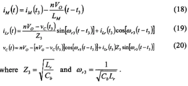
(14)Stage 4 [t&]: After the output rectifier starts to conduct at t3, iDl is the difference between iM and iLr multiplying by
the turns ratio of TX. The state equations can be written as follows: diM L -=-nVo dt *c - C
-
- iLr.
dt (18) ib(t)= 3 sm[w,,(t-t,)]+i,,(t,)cos[w,,(t-t,)] (19) vc(t)= nv, -[nv, -vc(t3)lcos[q3(r -r3)]+ib(t3p3 s i n [ q 3 ( t - t 3 ) ] (20) i, ( t ) = i , (t3)- -(t nV0 - t , ) L ,nv,
- v (t)
. z3 1 where Z3 = -K
and or3 =-a'
Stage 5 [k-t5]: S2 turns off at t4. The current of L, discharges CA, and Vhdecreases. This stage ends when the antiparallel diode of SI starts to conduct at t5. The output rectifier still conducts at t5, because the resonant inductor limits the discharging rate of iLr. The state equations can be written as follows: C , - - - - l *c - . C , - - i
*,
- dt Lr dt L r ' Solving (2 1)-
(24) yields: (25) (26) i , ( t ) = i , ( t 4 ) --
nV0 (t-
t,)
"Jt) = [-I&)+ n v 0 ] Q 5 {I - cos[w,4(t -t4)]+i,('*) sitl[q4(t - t 4 ) ] + 4 t 4 ) L , -v&4)+nVo ' sm[w,,(t - t 4 ) ] + iL,(t4)cos[q4(t
-
t 4 ) ] z4 'b %b' (27) (28) 1where Z, =
d
-
and or, =c,
Lr I1c,
J E z z
Stage 6 [ts-k]: At t5, Vh has dropped to zero and the antiparallel diode of SI is conducted. Before
iL,
changes direction, SI can be turned on under ZVS. The equations describing the circuit operation during this stage are as follows: di,-
diLr L,-
- -nVo L,-
=V ,
- v,+
nVo dt dt dt Cb-*,
--
i L , .Solving (29)
-
(3 l), we can obtain:i,(t)= i M ( t 5 ) - - ( t - t s ) nV0 L M Solving (1 5)
-
(17) yields:(t
-
2s>I+
i b (ts >c0sbr3 (t-
ts>I
( 3 3 ) .&)=
[ v ~
- ~ c ( ~ s l + ~ ~ o X ~
-~oslw,,(r-r,lD+i~,(r,~~ ~in[w,,(r-r,lI+~,(r,)(34) Stage 7 [t&]: At
k,
SI turns on under ZVS. The resonant inductor current iL, increases rapidly. This stage ends when this current increases to the point where the output rectifier cuts off. The dc input power source begins to charge cb, L,, and LM again. Another switching cyclestarts.
K n -vc(4>+"vo
z
3
i,,
(4
=111. ANALYSIS
According to the above analysis, this section will quantitatively analyze the key characteristics of this converter.
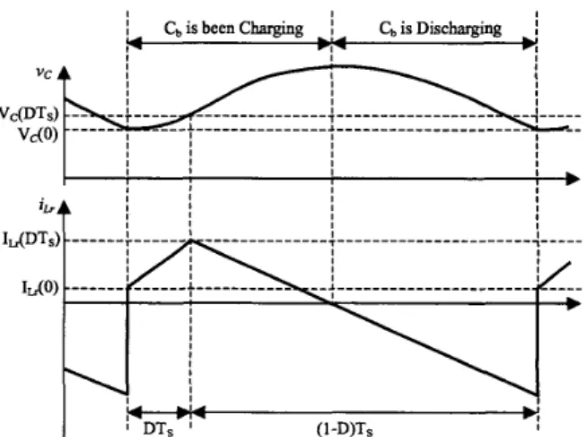
A. Energy-storage elements: The energy-storage elements in this converter consist of the blocking capacitor, the magnetizing inductor of Tx7 and the resonant inductor.
Fig. 4 shows the simplified waveforms of the voltage across the blocking capacitor and the current of the resonant inductor. During the interval DTs, the dc input power source charges cb, LM, and L,, causing the
increments in the voltage across cb as well as the current of LM and L,. Energy stored in these elements can be expressed as:
1
ELM + = (LM + Lr )['LIZ (0's -'LIZ
(011
(35)The incremental voltage across c b for this duration can be expressed as:
Inserting (38) into (35) yields:
ELM
+
EL, =G
'
DT' [2Kn-
(Vcb (DT' )+
Vc, (O))].
(39) 2 nCombining (36) and (37), we can obtain:
Ecb = i ~ D T s [ V c b ( D T s ) + V c b ( 0 ) ] 2 n (40) From (39) and (40), the total energy stored during the interval DTs is I I I CbisbeenCharging n T C,isDischarging j I I I I I 8 y (1-D)Ts I
Fig. 4. Simplified waveforms of the voltage across the blocking capacitor and the current of the resonant inductor.
When the voltage ripple across the blocking capacitor is neglected, (39) and (40) can be further condensed into ELM
+
ELI.=
--
1 Io DT, [2Kn-
2qn,0] = PoT,(l- D ) (42)2 n
(43)
Ecb
=
-2 DTs(2KnD) = PoTsD.
Equations (42) and (43) clearly describe the relationships between the amount of stored energy and the duty cycle.
During another interval (l-D)Ts, part of the energy stored in LM and L, transfers to the secondary side of Tx and the rest energy charges c b . After the resonant
inductor current changes direction, the energy stored in
cbtransfers to the output capacitor via Tx.
1 I
2 n
B. Z V S condition: The ZVS mechanism of S2 is alike a
linear charging process. According to (10) in section
II
,the ZVS condition of S2 can be obtained v, ( t ) =
(K,,
-
.,(Il))-
(1-
cos[wF2(t-
t,)Dc,
For Cb >> C, and ~ , ~ ( ? - f ~ ) small that sin[w,,(t-t1)]=ur2(t--t,) and COS[U,,(?-?~)]= 1
,
we get an approximate solution:(45) From (45), the Z V S operation of S2 can always be maintained when a sufficiently long dead time between the two power switches is used. The required dead time to achieve ZVS operation of S2 can be obtained by (45). The Z V S condition of SI depends on the energy stored in L,, which is quite different with S2. It can be obtained from (28) in section
II
:+-sin[q4(t-t4)]+V, iLr (f4
)
I O . (46)%Cds
Owing to the angular frequency, U,, , is much bigger than
w,,
, we cannot assume that 1-
cos[o,,(t - t,)] = 0 and omit this term just like the way in the previous case. However, this term can still be omitted because its coefficient is negligible when compared with that of the other terms. Therefore, (46) can be further simplified into(47) We can rearrange (47) to give
Solving (48), the ZVS condition of SI can be obtained:
1 1
- L 2 r L r i (t
>-c,v,,Z.
2 (49)
From (49), the ZVS condition of
SI
depends on the energy stored in L,.IV. EXPERIMENTAL RESULTS
To experimentally characterize the circuit behavior of the studied converter, a prototype was built to the specifications listed below:
switching frequencyfs: 60 kHz; input voltage Vi,: 400 Vdc; output voltage V,: 5 Vdc; maximum load current: 20 A; ZVS range: 0% to 100% load.
The power stage consists of the following parameters: diode DZ: 2xToshiba 30GWJ2C42C;
blocking capacitor Cb: 3.3uFI250V; input capacitor: 68uFl450V; Transformer:
switches SI and S2: Toshiba 2SK2842;
A , of core: 1 cm2;
primary: 36 turns of litz wire 2OxO.lmm; secondary: 3 turns of litz wire 100x0. lmm; resonant inductance, L, : 18 u H
(includes Llk and an external inductance); (between the turn-off of SI and turn-on of S2); LM: 280
a,
Llk: 8 UH;9 dead time: lOoUs
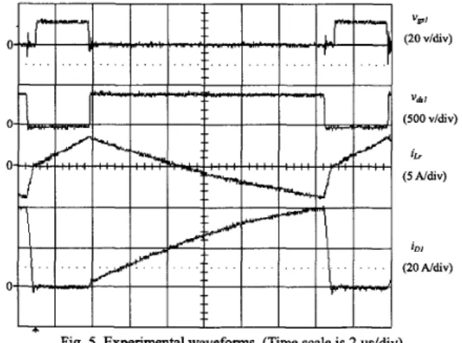
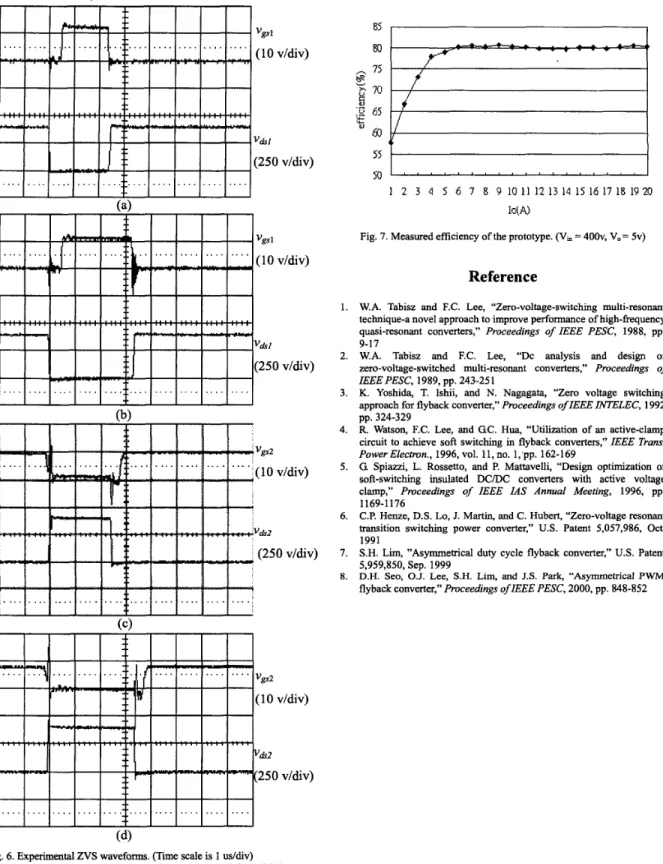
Some key experimental waveforms are shown in Fig. 5. These waveforms resemble closely those shown in Fig. 3. The ZVS operations of SI and S2 can be noted form the waveforms shown in Fig. 6. From Fig. 6(a) and 6(c), the converter remains ZVS operations of SI and S2 even under no load condition. The efficiency of the prototype is plotted in Fig. 7.
v.
SUMMARYFrom the analytical and experimental results, several circuit features have been observed as follows:
A. Not only the magnetizing inductor of the transformer and the resonant inductor, but also the blocking capacitor store energy when the output rectifier is off. When the duty cycle increases, the energy stored in the blocking capacitor will also increase accordingly. However, the energy stored in the magnetizing inductor and the resonant inductor will decrease. Most of the energy is stored in the blocking capacitor when the duty cycle exceeds 50%.
B. The ZVS conditions of these two power switches are quite different. The ZVS operation of S2 can always be maintain when a sufficiently long dead time between
SI
and S2 is used. However, SI achieves ZVS only when the energy stored in L, is larger than that of C.,
This paper describes the circuit behavior of the asymmetrical half bridge flyback converter. A detail analysis and mathematical equations have been given. A 5V120A prototype has been built to verify the analytical results. The experimental results show that the power switches can maintain ZVS operations from no-load to full-load and that the efficiency can reach an optimum value of 80%. V S J (20 v/div) V h l (500 v/div) L (5 Aldiv) .,.
85
so
h 75 E 2. 70 B2
65 k w ’ 6 0 5s M ddiv) v/&v) 1, “ ‘ ~ ‘ “ ” ‘ ‘ ~ ” ’ “ ’Fig. 6. Experimental ZVS waveforms. (Time scale is 1 us/div) (a) S1 at no load; @) S1 at full load; (c) S2 at no load ;(d) S2 at full load.