Effect of Structural Imperfections on the Excitonic Energy
Diamagnetic Shift on Self-assembled InAs/GaAs Nano-rings :
A Theoretical Approach
Effect of Structural Imperfections on the Excitonic Energy Diamagnetic
Shift in Self-assembled InAs/GaAs Nano-rings :
A Theoretical Approach
Student
Wei-ting Chiu
Advisor
Oleksandr Voskoboynikov
A Thesis
Submitted to Department of Electronics Engineering and Institute of electronics College of Electrical and Computer Engineering
National Chiao Tung University in partial Fulfillment of the Requirements
for the Degree of Master
in
Electronics Engineering November 2010
Hsinchu, Taiwan, Republic of China
脫
脫
脫 脫脫脫脫脫脫脫脫脫脫脫脫脫脫脫脫脫脫脫脫脫脫脫脫脫脫脫脫脫脫脫脫脫脫脫脫脫脫脫脫脫脫 脫 脫 脫 脫 脫 脫脫
脫脫
脫
脫 脫脫脫脫 脫
脫 脫 脫 脫 脫脫
Effect of Structural Imperfections on the Excitonic Energy Diamagnetic
Shift in Self-assembled InAs/GaAs Quantum Rings :
A Theoretical Approach
Student: Wei-ting Chiu Advisor: Prof. Voskoboynikov
Department of Electronics Engineering and
Institute of Electronics
National Chiao Tung University
ABSTRACT
In this study we calculate the excitonic energy diamagnetic shifts in self-assembled semiconductor nano-rings using the mapping and exact diagonalization methods. The mapping method allows a three dimensional description of the ring and the exact diagonalization method gives a way to compute the excitonic energies and wave functions. We start from symmetrically wobbled quantum rings with the electronic confinement potentials possessing a reflectional symmetry on the $(110)$ plane. The structural imperfections are considered by applying small variations on the geometry and potential profile and thus the reflectional symmetry is broken. Our results show that with small structural imperfections the excitonic wave functions will be located in one of the potential valleys and the extension of the wave functions will shrink greatly. A dramatical decrease in the excitonic energy diamagnetic shift is observed because the diamagnetic shift depends on the effective area spanned by the excitonic wave function. The calculated excitonic ground state energies and diamagnetic shift coefficients are in good agreement with the experimental measurements.
脫脫脫脫脫脫脫脫脫脫 脫
脫
脫
Thu
Contents
List of Figures . . . ii
List of Tables . . . iii
Chapter 1 Introduction . . . 1
Chapter 2 Theory . . . 3
2.1 Description of the System . . . 3
2.2 Mapping Method . . . 7
2.3 Exact-diagonalization of the Excitonic Hamiltonian . . . 8
2.4 Definition of the Diamagnetic Shift Coefficients . . . 9
2.5 Mesh Grids and the Calculation Details . . . 10
Chapter 3 Results and Discussion . . . 14
Chapter 4 Conclusion and Future Work . . . 24
4.1 Conclusion . . . 24
4.2 Previous Works . . . 24
4.3 Future Work . . . 25
List of Figures
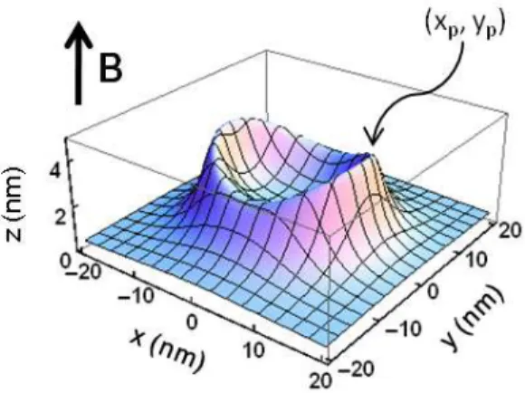
2.1 Geometry of a symmetrically wobbled nano-ring with uniform magnetic field
applied in z-direction. . . 4
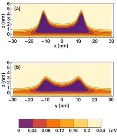
2.2 Contour plot of the electronic confinement potential of a symmetrically
wob-bled ring. The potential is projected onto (a) the x-z plane and (b) the y-z plane. 5
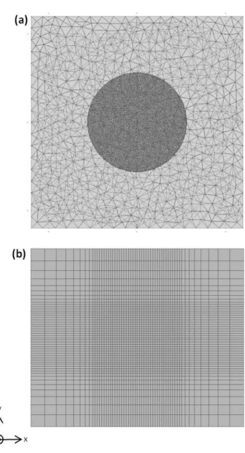
2.3 Top view of the meshes. (a) The mesh is generated randomly by COMSOL multiphysics package with 219,009 mesh points. (b) The mesh is controlled
and used in our simulation with 92,169 mesh points. . . 13
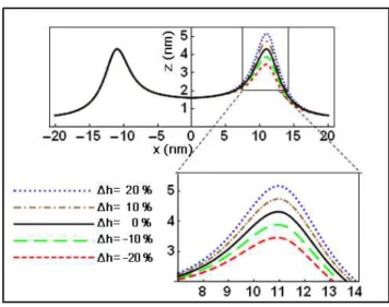
3.1 The ring’s height profiles with different ∆h. The ring’s heights are unchanged
along the negative x-direction. . . 16
3.2 Projections of the electronic confinement potential onto x-z plane, the posi-tive x direction is shown. (a): potential of a symmetrically wobbled ring; (b): ∆h=20%, ∆V =0; (c): ∆h=-20%, ∆V =0; (d): ∆h=0%, ∆V =0.2; (e): ∆h=0%,
∆V =-0.2. . . . 17
3.3 Projections of electronic potential on x-z plane changing both ∆h and ∆V . (a):
∆h = ∆V = 0; (b): ∆h=20%, ∆V =0.2; (c): ∆h=-20%, ∆V =-0.2. . . . 18
3.4 Probability densities for the excitons confined in nano-rings, projected onto the x-y plane with (a) ∆h = ∆V = 0, (b) ∆h = -10% and ∆V = -0.1 and (c) ∆h = 10% and ∆V = 0.1. (d) the height profile of a symmetrically wobbled ring and gives a reference for the location of the exciton probability densities. The
dashed lines indicate the position at x = 11.5nm and x = -11.5nm. . . 19
3.5 The excitonic transition energies with different (a) ∆h and (b) ∆V . The dashed
lines indicate the experimental measurement of excitonic energy: 1320 meV. . . 22
3.6 The excitonic transition energies when changing simultaneously both ∆h and ∆V . The dashed line indicates the experimental measurement of excitonic
List of Tables
3.1 Values of parameters used in this study. . . 15
3.2 Parameters for asymmetries. . . 15
3.3 Normalized coefficients of energy diamagnetic shift as a function on ∆h and ∆V . 20
3.4 Normalized coefficients of energy diamagnetic shift while changing both ∆h
Chapter 1
Introduction
In classical physics the magnetic response of a charged system is defined by the Lorentz force. Within the quantum domain the magnetic response of a ring structure shows an extraor-dinary result - the Aharonov-Bohm (AB) effect [1]. In some experiments the AB effect was clearly shown in the electronic energy spectra [2, 3] where magnetic dependent oscillations in the conductance and ground state energy were observed. Beside the experimental studies there were also theoretical investigations on the magnetic response of quantum-rings [4,5]. The magneto-optical properties of semiconductor nano-rings have called a considerable attention since the AB effect is not expected here because of the neutrality of exciton.
Recently, nano-ring structures were produced [8] and the magneto-excitonic ground-state behavior of a single quantum ring was observed [9]. According to the cross-sectional scanning-tunneling microscopy (X-STM) observations [8] those quantum rings are anisotropic in the height of the rim. Ring rim height in [110] direction is larger than in [110]. Also a mathematical description of the geometry was suggested. Although there is no longer a rotational symmetry within this model, an inherent reflectional symmetry on the (110) plane exists. However, even there is still a reflectional symmetry, when calculating the excitonic energy the separation of variables is impossible. Hence, the excitonic energy can be simulated on the base of a three dimensional description.
In this study we investigate the excitonic ground state energy and diamagnetic shift for quantum nano-rings and compare our results with the experimental measurements [9]. We should note that the diamagnetic shift coefficient [10,11] indicates the area spanned by the wave function of a particle confined to a system. In our simulation we found that the mathematical model with reflectional symmetry on the (110) plane would make the exciton wave function
equally distributed into the two potential valleys of the quantum ring’s potential. Nevertheless, the perfect reflectional symmetry of the system only exists in idealized mathematical model and there would always be some structural imperfections which break the reflectional symmetry. Therefore, to include the imperfections in the model we made adjustments for both the geometry and confinement potential of the quantum rings. Changing the height profile on one of the wobbled hills causes a wobbling asymmetry on the quantum ring, and a disbalanced potential is resulted in the different depths of one of the side potential valleys. Our result shows that with small deviations in the height profile and confinement potential on one side (the positive x side) of the ring, the distribution of the excitonic wave function would collapse into the corresponding potential valley, causing a drop on the excitonic energy diamagnetic shift coefficient.
This report is organized as follows: in chapter two we describe nano-ring systems in their geometry and confinement potentials, including structural imperfections into the mathematical model, and the simulation method is presented; the simulation results are discussed in chapter three; finally, we summarize our work and propose possible future works.
Chapter 2
Theory
2.1 Description of the System
To build a model of a quantum ring, we first assume that the ring is grown on a plane parallel to the x-y plane and an external magnetic field applied in z-direction. The height profile of the ring is taken from Ref. [12] which fits actual shape of a quantum ring. We modify it in order to apply in this study a wobbling asymmetry:
h(x, y) = h0+ [1 + ain· C(x, y)] · h e hM(x, y) − h0 i e γ0(x, y)2 ∆R(x, y)2+ eγ 0(x, y)2 ·R(x, y)e 2− ∆R(x, y)2 e R(x, y)2 , p x2+ y2 ≤ eR; h(x, y) = h∞+ [1 + aout· C(x, y)] · h ehM(x, y) − h∞ieγ ∞(x, y)2 ∆R(x, y)2 + eγ ∞(x, y)2 ,px2 + y2 > eR, (2.1) where C(x, y) = exp " −(x − xp) 2+ (y − y p)2 b2 # , (2.2) e hM(x, y) = hM µ 1 + ξx 2− y2 x2+ y2 ¶ , (2.3) e R(x, y) = R µ 1 + ξRx 2− y2 x2+ y2 ¶ , (2.4) ∆R(x, y) = px2+ y2− eR, (2.5) e γ0(x, y) = γ0 µ 1 + ξγx 2− y2 x2+ y2 ¶ , (2.6)
Figure 2.1: Geometry of a symmetrically wobbled nano-ring with uniform magnetic field ap-plied in z-direction. e γ∞(x, y) = γ∞ µ 1 + ξγx 2− y2 x2+ y2 ¶ . (2.7)
The parameters (xp, yp) indicate the ring’s peak positions on the rim (see fig. 2.1, as the arrow
pointed), b controls the range of wobbling asymmetry, ainand aout can be manipulated to give
different degree of wobbling asymmetries, and R is the radius of the rim. If ain = aout = 0 the
ring has a reflectional symmetry about x=0 plane and the wobbling is symmetric (see fig. 2.1 and Ref. [12]).
Using this geometry we create a corresponding electronic confinement potential:
Ve(x, y, z) = ∆E · 1 − 1 + tanh¡z a ¢ 2 · 1 −1 + tanh ³ z−h(x,y) a ´ 2 . (2.8)
This expression gives a slowly changing potential for electron confined in the ring which reflects the composition of InAs smoothly varying from inside (the ring’s indium-rich part) to outside.
From Fig. 2.2 it should noticed that unlike a conventional doubly-connected ring, this struc-ture is singly-connected since the center is not hollow. However, it still possesses some ring’s properties since the probability density of the exciton confined inside the ring, at the rim posi-tion is still higher than at the center part, thus it is a ring-like nano structure.
We assume that there are two reasons for the structural imperfections. The first one comes from a wobbling asymmetry of the height profile of the nano-ring. We can achieve such
geom-Figure 2.2: Contour plot of the electronic confinement potential of a symmetrically wobbled ring. The potential is projected onto (a) the x-z plane and (b) the y-z plane.
etry imperfections (wobbling asymmetry) by substituting different values of ain and aout. We
define the degree of the wobbling asymmetry ∆h on the rim of the ring by
∆h = h+− h−
h−
× 100%, (2.9)
where h+(h−) indicate the height at the peak’s positions on the rim in the +(-) x-direction. A
set of parameters {ain, aout} gives a value of ∆h.
Another origin of the structural imperfections is disbalanced potential valley depths along x-axis. To model the potential depth change on the positive x-side we define another expression for the electronic confinement potential
Ve(x, y, z) = ∆E · 1 − 1 + tanh¡z a ¢ 2 · 1 −1 + tanh ³ z−h(x,y) a ´ 2 (2.10) · 1 − 1 + tanh ³ x−bV bV ´ 2 + 1 − 1 + tanh ³ xV−x bV ´ 2 +∆E · 1 − (1 + ∆V ) · 1 + tanh¡z a ¢ 2 · 1 − 1 + tanh ³ z−h(x,y) a ´ 2 · 1 − 1 + tanh ³ x−bV bV ´ 2 · 1 − 1 + tanh ³ xV−x bV ´ 2 ,
where xV and bV controls the range of the disbalanced potential, and ∆V indicates the value of
disbalance. The potential on the negative x-side is unchanged.
The value ∆V reflects the indium composition (c of IncGa1−cAs) difference along x-direction.
We can set ∆V = 0.1 when the composition at the peak position at the rim of the ring on the positive x-direction is 10% more than on the negative x side. By varying ∆h and ∆V we build a model of nano-rings with two kinds of structural imperfections: the wobbling asymmetry in the geometry and disbalanced confinement potential.
2.2 Mapping Method
In order to have a unified parameter following the geometry and composition changes we define the mapping function [14] as follows:
M(x, y, z) = 1 − Ve(x, y, z)
∆Ee
. (2.11)
Using this function we can further obtain other position-dependent material parameters by the following interpolations:
m∗
e(h)(x, y, z) = m∗e(h),in· M(x, y, z) + m∗e(h),out· [1 − M(x, y, z)] , (2.12)
²(x, y, z) = ²in· M(x, y, z) + ²out· [1 − M(x, y, z)] ,
Eg(x, y, z) = Eg,in· M(x, y, z) + Eg,out· [1 − M(x, y, z)] ,
where m∗
e(h) is the electron (hole) effective mass, ² is the permittivity, and Eg is the energy gap.
The subscription of in and out indicate the corresponding inside (InAs) and the outside (GaAs) material parameters.
The hole confinement potential can be obtained from the electronic potential and the energy gap:
Vh(x, y, z) = Eg(x, y, z) − Ve(x, y, z) − Eg,in. (2.13)
The mapping procedure gives a full three-dimensional description of this ring-like structure. All the material parameters are mapped by the mapping function and hence they follow the exper-imental informations about geometry and composition of the structure. We can then solve the corresponding exciton problem to find the excitonic energy and corresponding wave function using the above position-dependent parameters.
2.3 Exact-diagonalization of the Excitonic Hamiltonian
To obtain the excitonic energy and wave function of the system we implement the exact-diagonalization method [15, 16]. This method uses the non-interacting electron and hole wave functions as basis to expand the excitonic wave function and then diagonalize the excitonic Hamiltonian.
The exciton Hamiltonian is expressed as: b
HX = bHe+ bHh− e2G(re, rh), (2.14)
where G(re, rh) is the Green’s function of the Poisson equation
²0∇r[²(r)∇rG(r, r0)] = −δ(r − r0), (2.15)
²(r) is the position dependent permittivity defined in previous section, bHeand bHh are the
non-interacting electron and hole Hamiltonians: b He(h) = 1 2Π e(h) r à 1 m∗ e(h)(r) ! Πe(h)r + Ve(h)(r), (2.16)
where Ve(h)(r) and m∗e(h)(r) are the electronic (hole) confinement potential and effective mass,
Πe(h)r = −i~∇r+ (−)eA(r) is the momentum operator for electron (hole), A(r) is the vector
potential of the magnetic field B(r) = ∇ × A(r) and e is the absolute value of electron charge. We ignore the electron and hole spins in this study. Solving the above non-interacting problems
we obtain the vector spaces for electron and hole Λe(re) and Λh(rh) which are spanned by the
non-interacting electron and hole basis {Fel(re)} and {Fhk(rh)}, where el and hk represent the
main quantum numbers of the electron and hole. The excitonic wave function can be expanded by the non-interacting electron and hole basis:
ΨX(re, rh) =
X
i
where i indicates the set of certain possible transitions: {el; hk}. We obtain the excitonic energy
EX from the following secular equation
det£(Eel+ Ehk+ Eg,in− EX) δij − e2Gij
¤
= 0. (2.18)
The coefficient ai can be obtained from:
X j © (Eel+ Ehk+ Eg,in) δij − e2Gij ª · aj = EXn · ai, (2.19) where Gij = Z Fel(re) Fel0(re) Vhk;hk0(re)dre, (2.20)
and we can possess Vhk;hk0(re) by solving the Poisson equations for all sets {hk, hk0}:
²0∇r[² (r) ∇rVhk;hk0(r)] = −Fhk(r) Fhk0(r). (2.21)
2.4 Definition of the Diamagnetic Shift Coefficients
To calculate the diamagnetic shift we choose the following gauges for the vector potential [17]:
A(re) = 1
2B × (re− re); A(rh) =
1
where re= (xe, ye, ze) and rh = (xh, yh, zh) with xe = hψX|xe|ψXi; (2.23) ye = hψX|ye|ψXi; ze = hψX|ze|ψXi; xh = hψX|xh|ψXi; yh = hψX|yh|ψXi, zh = hψX|zh|ψXi,
those are the expectation values of the electron and hole positions.
With the above gauges in the low-field limit and B applied in the z-direction we can approx-imate the energy shift of the exciton in ground state as
∆E ≈ γB2, (2.24)
where γ is the diamagnetic shift coefficient which can be calculated through
e2 8 µ h(x − xe) 2+ (y − y e)2 m∗ e i + h(x − xh) 2+ (y − y h)2 m∗ h i ¶ . (2.25)
The numerator of the expectation values in Eq. (3.15) is the effective extension for the electron and hole confined in the ring, and thus corresponds to the actual lateral confinement of the exciton. Thus by calculating γ we can possess the knowledge of the distribution of the excitonic wave function and actual position of the exciton in this system.
2.5 Mesh Grids and the Calculation Details
The mesh grids is important in this simulation since there is two equaled valleys while using a mathematical model. The ground state wave function of a particle confined in the potential
with two balanced valleys is expected to extend into the both potential valleys equivalently. According to our computation experiences, if the density of the mesh is inadequate or not fol-lowing the reflectional symmetry the calculated wave function of the particle will not reveal such symmetry.
We build the model of the ring using COMSOL multiphysics package (www.comsol.com). This package can generate meshes automatically and conveniently, but the meshes produced are not always decent and balanced for a full three dimensional calculation. While solving our problem in ideal situation we should have a mesh with infinitesimal distance between every two mesh points so a exact result can be obtained. However, practically due to machine power and memory limitations we can only produce a mesh with distances between every two mesh points as small as possible to reduce the error. In this study we monitor the error which comes from mesh by looking into the terms of (2.20). For example, due to a reflectional symmetry (while there are no structural imperfections) the term
G12=
Z
Fe1(re) Fe2(re) Vh1;h1(re)dre= 0. (2.26)
Since Fe1(re) and Vh1;h1(rr) are even functions and Fe2(re) is odd (the potential is an even
function due to reflectional symmetry, so the ground state of the particle in the potential is even and the first excited state is odd), ideally the above term should be zero. However, if we use the mesh produced automatically by the package with only 59,711 mesh points the value of the
term is in an order of 10−7 eV which is close to the energy diamagnetic shift with an order of
10−6 eV in low magnetic field. Therefore, an error rises while the mesh is not appropriately
defined.
There are two possible ways to eliminate the error caused by the mesh. The first one is by increasing the mesh size, thus the distance between mesh points decreases. But at the same time requirements for machine power and memory are getting to physical machine limits. If the mesh is generated with an upper bound of 1.02 nm for the distance between two mesh points in the central part of the simulation domain, the calculated electron and hole wave function can
in total can only be used to calculate electron and hole separately, because of the limitation of the machine memory we can not involve enough large number of electron and hole states to expand the excitonic wave function for our a system. Hence we choose an adaptive mesh grids as shown in Fig. 2.3. The distance between mesh points in the central part within a region 50nm×40nm×20 nm is 1.25nm. This mesh follows the symmetry of the system and minimizes the disbalance in the particles’ wave function with the value of (2.26) reduced to an order of
10−15eV which gives a good accuracy. We shorten the length of the outside domain (relative
to the center part) to reduce the requirement of machine power. The particles’ wave functions are localized in the central part and they are more extended in x-direction than in y-direction, thus decreasing the domain length in y-direction causes only negligible errors. For consistency of this work we keep the same mesh upon changing the value of ∆h and ∆V . The simulation is performed within a domain with edges 120nm×80nm×80nm with 92,169 mesh points in total.
In this study we take five electronic states and five hole states to expand the exciton wave function since there are only five electron states confined in the system while the structural im-perfections are not included. We find the convergence by keeping the same number of electron states and increasing the number of hole states. The difference of the exciton ground state en-ergy when we take five hole states or four hole states to expand the exciton wave function is
only in an order of 10−7 eV. Therefore, we take five hole states as well. In order to maintain
a consistency in this work we keep the same computational configuration while varying the values of ∆h and ∆V .
Figure 2.3: Top view of the meshes. (a) The mesh is generated randomly by COMSOL multi-physics package with 219,009 mesh points. (b) The mesh is controlled and used in our simula-tion with 92,169 mesh points.
Chapter 3
Results and Discussion
We use the parameters for the height profile as suggested in Ref. [12] and c = 0.55 is chosen
to be the indium content in the IncGa1−cAs quantum ring. Material parameters such as effective
masses, band gaps for electron and hole in strained InAs is taken from Ref. [13]. All values
of the parameters are listed in Table 3.1. m0 stands for the electron rest mass and ²0 is the
permittivity in vacuum.
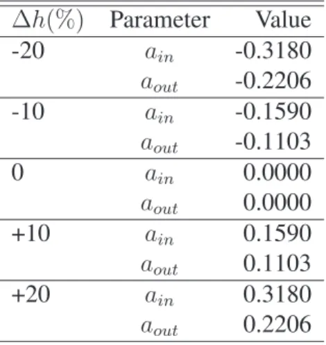
The structural imperfections are included in this work by considering ∆V = -0.2, -0.1, 0, 0.1, 0.2 (we use (2.8) while ∆V =0 and (2.10) when ∆V 6= 0 ) and ∆h = -20%, -10%, 0%,
10%, 20% with appropriate sets of {ain, aout} listed in Table 3.2. While varying ∆h both the
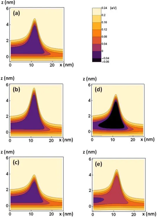
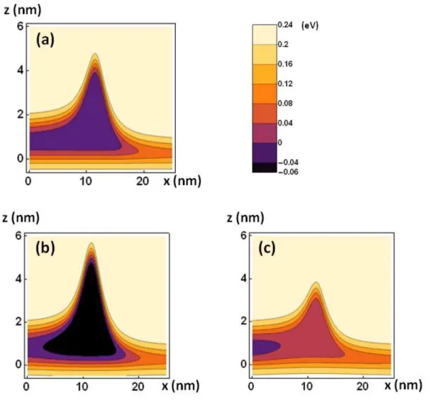
geometry and the confinement potential alter (see Fig. 3.1 and 3.2). Changes in the confinement potential due to changes of ∆V is depicted in Fig. 3.2(d) and 3.2(e). In Fig. 3.3 we present the electronic confinement potentials with both ∆h and ∆V varying.
From our simulation we found that when the potential is symmetric about x=0 plane the exciton wave function are distributed equally within two valleys of the potential at the ring’s rim. However, when we induce small variations in either the ring’s geometry or the potential the wave function collapses into one of the valleys, as a consequence, the spread of the probability distribution of the exciton shrinks.
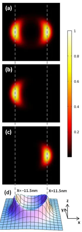
Fig. 3.4 demonstrates the probability density of the excitons confined in the quantum ring. While there is no wobbling asymmetry the wave function extends to both valleys equally ( see Fig. 3.4(a) ). If we impose a structural imperfection either by decreasing ∆h or ∆V with 10% of their original value the exciton tends to be stay in the valley on the negative x side ( Fig. 3.4(b) ). If we increase each of ∆h or ∆V the wave function of the exciton collapses into another valley ( Fig. 3.4(c) ).
Table 3.1: Values of parameters used in this study.
Parameter Value Parameter Value
†m∗ e,in 0.054 m0 R 10.75 nm m∗ e,out 0.067 m0 γ0 3 nm †m∗ h,in 0.266 m0 γ∞ 3 nm m∗ h,out 0.500 m0 hM 3.6 nm †E g,in 0.147 eV h0 1.6 nm Eg,out 1.159 eV h∞ 0.4 nm †∆E 0.230 eV ξ 0.2 †² in 14.138 ²0 ξγ -0.25 ²out 12.900 ²0 ξR 0.07 xp 11.5 nm b 6 nm yp 0 nm bV 4 nm xV 18.5 nm
†Parameters inside the In
cGa1−cAs/GaAs ring
are taken by interpolation.
Table 3.2: Parameters for asymmetries.
∆h(%) Parameter Value -20 ain -0.3180 aout -0.2206 -10 ain -0.1590 aout -0.1103 0 ain 0.0000 aout 0.0000 +10 ain 0.1590 aout 0.1103 +20 ain 0.3180 aout 0.2206
Figure 3.1: The ring’s height profiles with different ∆h. The ring’s heights are unchanged along the negative x-direction.
We know that the diamagnetic shift coefficient (γ) is proportional to the effective area spanned by the exciton wave function, therefore, if the extension of the exciton wave function decreases the coefficient drops as well. We define γ(∆h, ∆V ) as a function of the parameters ∆h and ∆V and present with the ratio of γ(∆h, ∆V ) to γ(0, 0). We calculate γ with varying only one parameter for the structural imperfection and the ratio is shown in table 3.3. The result demonstrates that with either a small variation in the wobbling asymmetry or a small disbal-anced potential lead to decrease of γ. In table 3.4 we show the ratio while both the wobbling asymmetry and the disbalanced potential are considered, and we obtain the same tendency for
Figure 3.2: Projections of the electronic confinement potential onto x-z plane, the positive x direction is shown. (a): potential of a symmetrically wobbled ring; (b): ∆h=20%, ∆V =0; (c): ∆h=-20%, ∆V =0; (d): ∆h=0%, ∆V =0.2; (e): ∆h=0%, ∆V =-0.2.
Figure 3.3: Projections of electronic potential on x-z plane changing both ∆h and ∆V . (a): ∆h = ∆V = 0; (b): ∆h=20%, ∆V =0.2; (c): ∆h=-20%, ∆V =-0.2.
Figure 3.4: Probability densities for the excitons confined in nano-rings, projected onto the x-y plane with (a) ∆h = ∆V = 0, (b) ∆h = -10% and ∆V = -0.1 and (c) ∆h = 10% and ∆V = 0.1. (d) the height profile of a symmetrically wobbled ring and gives a reference for the location of the exciton probability densities. The dashed lines indicate the position at x = 11.5nm and x = -11.5nm.
Table 3.3: Normalized coefficients of energy diamagnetic shift as a function on ∆h and ∆V . ∆h(%) γ(∆h, 0)/γ(0, 0) ∆V γ(0, ∆V )/γ(0, 0) -20 0.32 -0.2 0.31 -10 0.35 -0.1 0.32 0 1.00 0 1.00 10 0.29 0.1 0.29 20 0.28 0.2 0.27
Table 3.4: Normalized coefficients of energy diamagnetic shift while changing both ∆h and ∆V . ( ∆h, ∆V ) γ(∆h, ∆V )/γ(0, 0) (-20%, -0.2) 0.33 (-10%, -0.1) 0.35 ( 0%, 0 ) 1.00 ( 10%, 0.1 ) 0.26 ( 20%, 0.2 ) 0.23
Notice that when we decrease either ∆h or ∆V , the ratio γ(∆h, ∆V )/γ(0, 0) approaches 0.3. Because for those changes the excitonic wave functions are located at the unchanged potential valley, the effective areas spanned by the excitonic wave functions are similar no matter which parameter we decrease. The same results appear while we decrease both the parameters simultaneously (see table 3.4), which supports our arguments. However, if ∆h and ∆V continue increasing γ keeps dropping. When we enhance both ∆h and ∆V to 20% and 0.2 respectively the ratio γ(∆h, ∆V )/γ(0, 0) approaches 0.23 and the calculated excitonic
energy diamagnetic shift coefficient reaches 10 µeV /T2. The reason for the minification of γ
is that the confinement is stronger when imposing two kinds of imperfections than considering only one of them, thus the extension of the exciton wave function is more restricted inside the valley which the structural imperfections are applied. The result conforms with the experimental
measurement of a averaging value of 6.8 µeV /T2 [9].
The calculated excitonic ground state energies are shown in Fig. 3.5 and Fig. 3.6. With a symmetrically wobbled ring and balanced confinement potential the excitonic ground state
en-ergy is about 1360 meV which is higher compared with the energies when imperfections are ap-plied. The coulombic interaction between electron and hole is smaller due to a wider extension of excitonic wave function when the excitonic wave function is distributed into both potential valleys, therefore the excitonic ground state energy is higher. If we impose structural imper-fections the excitonic ground state energy would go down because now the exciton is located in one of the potential valleys and the coulombic interaction is stronger because of a reduced extension of the excitonic wave functions. While we decrease either ∆h or ∆V the energies reach 1350 meV (see Fig. 3.5 and 3.6). Because the excitons stay now in the unchanged poten-tial valley, the energies saturate while the degree of the imperfections become larger. However, when the imperfections are imposed involving a raise of ∆V the exciton ground state energies continue dropping. Since in this situation the exciton locates in the valley where the potential depth is decreasing, the excitonic energies are dropping as ∆V increasing. The calculated ex-citonic ground state energies range from 1300 meV to 1340 meV while disbalanced potentials are imposed and the results consist with the experimental measurement of 1320 meV [9].
Figure 3.5: The excitonic transition energies with different (a) ∆h and (b) ∆V . The dashed lines indicate the experimental measurement of excitonic energy: 1320 meV.
Figure 3.6: The excitonic transition energies when changing simultaneously both ∆h and ∆V . The dashed line indicates the experimental measurement of excitonic energy: 1320 meV.
Chapter 4
Conclusion and Future Work
4.1 Conclusion
In conclusion, we calculate the excitonic diamagnetic shift coefficients of wobbled and singly-connected InAs/GaAs semiconductor nano-rings using the mapping and exact-diagonalization methods. Beside a mathematically model with a reflectional symmetry in the confinement po-tential we introduce two possible structural imperfections - wobbling asymmetry and disbal-anced potentials - in our simulation. Within these approaches and taking an appropriate mesh we are able to describe this system. From our simulation we found that with small deviations in the geometries and confinement potentials the excitonic diamagnetic shift coefficient decreases greatly. Our results are in a good agreement with the experimental measurings.
4.2 Previous Works
In Ref. [18] we calculated the excitonic and biexcitonic energies of InAs/GaAs nano-rings with geometry suggested in Ref. [8] and radius 7 nm. The problem was solved self-consistently using our mapping method, and we obtained preliminary results about this nano structure. After that we implemented the diagonalization method and calculated the magnetic response of rings in a weak magnetic field with an asymmetry in the geometry, this result was published in Ref. [19]. The magnetic susceptibility of wobbled semiconductor nano-rings were calculated in Ref. [20], and we found that the averaged susceptibility shows small temperature effect. The mapping method was used to calculate the energy of concentric triple nano-rings as well, and the calculated inhomogeneous broadening of the excitonic energy peaks was found in a good agreement with the experimental data [21].
4.3 Future Work
It is interesting to figure out the effect of structural imperfections on the diamagnetic shift coefficient of biexciton, and it can be compared with experimental measurement [9]. The
reac-tion of charged excitons such as X+ and X− (exciton with an extra electron or a hole) in the
References
[1] Y. Aharonov and D. Bohm, ”Significance of Electromagnetic Potentials in the Quantum
Theory,” Physical Review 115, 485 (1959).
[2] A. Lorke, R. J. Luyken, A. O. Govorov, J. P. Kotthaus, J. M. Garc´ıa and P. M. Petroff,
”Spectroscopy of Nanoscopic Semiconductor Rings,” Physical Review Letters 84, 2223 (2000).
[3] A. Fuhrer, S. L¨uscher, T. Ihn, T. Heinzel, K. Ensslin, W. Wegscheider and M. Bichler,
”Energy spectra of quantum rings,” Nature (London) 413, 822 (2001).
[4] O. Voskoboynikov, Y. Li, H. -M. Lu, C -F. Shih, and C. P. Lee, ”Energy states and
magne-tization in nanoscale quantum rings,” Physical Review B 66,155306 (2002).
[5] M. Aichinger, S. A. Chin, E. Krotscheck, and E. R¨as¨anen, ”Effects of geometry and
im-purities on quantum rings in magnetic fields,” Physical Review B 73, 195310 (2006).
[6] O. Voskoboynikov, C. M. J. Wijers, J. L. Liu, and C. P. Lee, ”Magneto-optical response
of layers of semiconductor quantum dots and nanorings,” Physical Review B 71, 245332 (2005).
[7] D. Haft, C. Schulhauser, A. O. Govorov, R. J. Warburton, K. Karrai, J. M. Garcia, W.
Schoenfeld, P. M. Petroff, ”Magneto-optical properties of ring-shaped self-assembled In-GaAs quantum dots,” Physica E 13, 165 (2002).
[8] P. Offermans, P. M. Koenraad, J. H. Wolter, D. Granados J. M. Garc´ıa, V. M. Fomin, V. N.
Gladilin, and J. T. Devreese, ”Atomic-scale structure of self-assembled InGaAs quantum rings in GaAs,” Applied Physics Letters 87, 131902 (2005).
[9] T. -C. Lin, C. -H. Lin, H. -S. Ling, Y. -J. Fu, W. -H. Chang, S. -D. Lin, and C. -P. Lee,
”Impacts of structural asymmetry on the magnetic response of excitons and biexcitons in single self-assembled In(Ga)As quantum rings,” Physical Review B 80, 081304(R) (2009).
[10] S. N. Walck and T. L. Reinecke, ”Exciton diamagnetic shift in semiconductor
nanostruc-tures,” Physical Review B 57, 9088 (1998).
[11] M. Grochol, F. Grose, and R. Zimmermann, ”Exciton wave function properties probed by
diamagnetic shift in disordered quantum wells,” Physical Review B 71, 125339 (2005).
[12] V. M. Fomin, V. N. Gladilin, S. N. Klimin, J. T. Devreese, N. A. J. M. Kleemans and P.
M. Koenraad, ”Theory of electron energy spectrum and Aharonov-Bohm effect in
self-assembled InxGa1−xAs quantum rings in GaAs,” Physical Review B 76, 235320 (2007).
[13] C. E. Pryor and M. -E. Pistol, ”Band-edge diagrams for strained III–V semiconductor
[14] L. M. Thu and O. Voskoboynikov, AIP Conference Proceedings 1233, 952 (2010).
[15] H. Hu, J. -L. Zhu, J. -J. Xiong, ”Energy levels and far-infrared spectroscopy for two
elec-trons in a nanoscopic semiconductor ring,” Physical Review B 62, 16777 (2000).
[16] L. M. Thu and O. Voskobonikov, ”Magneto-optics of layers of double quantum dot
molecules,” Physical Review B 80, 155442 (2009) .
[17] L. D. Landau and E. M. Lifshitz, ”The Classical Theory of Fields,” 4th revised English
edition, Pergamon Press Ltd (1975).
[18] L. M. Thu, W. T. Chiu, Shao-Fu Xue, Ta-Chun Lin, and O. Voskoboynikov, ”Binding
energy of magneto-biexcitons in semiconductor nano-rings,” Physics Procedia 3, 1149 (2010).
[19] L. M. Thu, W. T. Chiu, Ta-Chun Lin, and O. Voskoboynikov, ”Effect of geometry on the
excitonic diamagnetic shift of nano-rings,” accepted in Physica Status Solidi C, published online in 25 October 2010.
[20] L. M. Thu, W. T. Chiu, and O. Voskoboynikov, ”Temperature stable positive magnetic
sus-ceptibility of semiconductor wobbled nano ring,” Journal of Physics: Conference Series 245, 012042 (2010).
[21] L. M. Thu, W. T. Chiu, and O. Voskoboynikov, ”Inhomogeneous broadening of the
exci-tonic peaks for ensembles of concentric triple nano-rings,” submitted to Physical Review