國 立 交 通 大 學
電子工程學系 電子研究所碩士班
碩 士 論 文
不同前處理對氮氧化鉿(鋯)
閘極介電層於鍺基板之電物性研究
The Electrical and Physical Properties of Hf(Zr)-oxynitride Gate
Dielectrics on Ge Substrates with Various Surface Pretreatments
研 究 生:林 哲 弘
指導教授:張 俊 彥 博士
不同前處理對氮氧化鉿(鋯)
閘極介電層於鍺基板之電物性研究
The Electrical and Physical Properties of Hf(Zr)-oxynitride Gate
Dielectrics on Ge Substrates with Various Surface Pretreatments
研 究 生:林 哲 弘 Student:Je-Hung Lin
指導教授:張 俊 彥 博士 Advisor:Dr. Chun-Yen Chang
國 立 交 通 大 學
電子工程學系電子研究所碩士班
碩 士 論 文
A Thesis
Submitted to Department of Electronics Engineering & Institute of Electronics College of Electrical and Computer Engineering
National Chiao Tung University in partial Fulfillment of the Requirements
for the Degree of Master
in
Electronics Engineeing & Institute of Electronics
June 2006
Hsinchu, Taiwan, Republic of China
不同前處理對氮氧化鉿(鋯)
閘極介電層於鍺基板之電物性研究
研 究 生:林 哲 弘 指 導 教 授:張 俊 彥 博士
國立交通大學
電子工程學系 電子研究所碩士班
摘 要
對於四氟化碳和氨氣電漿前處理以及二矽乙烷的鈍化前處理方法,我
們有系統地研究此三種表面前處理對於氮氧化鉿以及氮氧化鋯閘極介電層
在鍺基板上之電物性。
我們發現高介電係數材料與鍺基板的接面和矽基板的接面有不同熱化
學的特性;在矽基板與氮氧化鋯之間的接面層會因高溫處理而成長,並且
有助於鋯金屬矽化物的形成。相反的,在鍺基板與氮氧化鋯之間的接面層
會因高溫處理而揮發,並且抑制鋯金屬鍺化物的形成,此外,由於接面層
揮發使介電層所產生的局部凹陷現象,亦會損害高介電係數材料/鍺基板元
件結構的電性。
高介電係數材料/鍺基板結構會有很差的熱穩定性主要是由於低品質的
鍺原生氧化層,因此沉積介電質後的熱退火處理以及沉積金屬電極後的熱
退火處理就被用來檢驗白金/高介電係數材料/鍺基板電容結構之熱穩定
性。我們發現沉積介電質後的熱退火處理並不會增加鍺基板的捕捉缺陷
( bulk traps ),而沉積金屬電極後的熱退火處理卻會使其增加。此外,這兩
種熱退火處理都能削減接面載子捕捉密度( D
it)與縮小等效氧化層厚度,但
此二種熱處理過程卻同時增加了閘極漏電流。
四氟化碳電漿前處理會使白金/高介電係數材料/鍺基板電容結構中的
遲滯寬度與閘極漏電流增大,這很可能是由於接面載子捕捉密度以及表面
粗糙度的增加。另一方面,氨氣電漿前處理卻壓縮了遲滯寬度,這應該與
較少的氧化鍺和接面載子捕捉密度有關,另外,此種氮化過程也能減少氧
化鍺的成長以及它的揮發,因而改善白金/高介電係數材料/鍺基板電容結構
的熱穩定性。
在攝氏五百五十度下熱脫附十分鐘以及接下來的二矽乙烷鈍化前處理
已經成功地消除鍺的原生氧化層,因此大大縮小了遲滯的寬度,但是在高
頻的電容-電壓曲線圖中,有經過二矽乙烷鈍化前處理的試片卻呈現出低頻
的電容-電壓特性曲線。然而,這些表面前處理解決了遲滯現象並且改善了
白金/高介電係數材料/鍺基板電容結構的熱穩定性,因此持續最佳化接面特
性應能改善電性以及實現鍺基板結合高介電係數材料之元件。
The Electrical and Physical Properties of Hf(Zr)-oxynitride Gate
Dielectrics on Ge Substrates with Various Surface Pretreatments
Student:Je-Hung Lin Advisor: Dr. Chun-Yen Chang
Department of Electronics Engineering and Institute of Electronics
National Chiao Tung University, Hsinchu, Taiwan
ABSTRACT
We have systematically investigated the electrical and physical properties of HfOxNy and
ZrOxNy gate dielectrics on Ge substrates with different surface pretreatments, including CF4
plasma pretreatment, NH3 plasma pretreatment and Si2H6 passivation.
We found that the interfacial layer of high-k/Si and high-k/Ge have distinct thermochemical properties; high temperature processing aided the interfacial layer growth and the formation of Zr–silicate in ZrOx(Ny)/Si gate stack. On the contrary, severe interfacial layer
volatilization and the inhibition of Zr–germinate were found in ZrOx(Ny)/Ge system,
moreover, the generated localized pits in deposited high-k films owing to the desorption of the interfacial layer might degrade the electrical properties of fabricated high-k/Ge devices.
stability of Pt/high-k/Ge capacitors. We found that the PDA process did not multiply the pre-existing bulk traps in Ge substrate but the PMA process increased them. Furthermore, both annealing processes were found to annihilate the amount of Dit and shrink the CET, but
these thermal processed increased the gate leakage current at the same time.
The CF4 plasma pretreatment enlarged the hysteresis width and gate leakage current of
Pt/high-k/Ge capacitors, which were possibly due to the increment of Dit and surface
roughness. On the other hand, the NH3 plasma pretreatment compressed the hysteresis width,
which was related with less GeOx and Dit, moreover, this nitridation process improved the
thermal stability of Pt/high-k/Ge capacitors by diminishing the formation of GeOx and their
volatilization.
The Ge native oxide was successful eliminated by thermal desorption at 550°C for 10
min and following Si2H6 passivation, which greatly reduced the hysteresis width of
Pt/high-k/Ge capacitors, but the high frequency C-V curves of the Si2H6 passivation samples
presented a low-frequency-like characteristic. However, those surface pretreatments solved the hysteresis effect and improved the thermal stability of Pt/high-k/Ge capacitors, thus the continuous optimization of the interface properties are expected to improve the electrical characterization and achieve the Ge device in combination with a high-k dielectric.
誌 謝
兩年的碩士班研究生活即將告一個段落,在這兩年之中,獲得了許多
的幫助與指導,也使得我的碩士生涯能夠順利進行,在此我必須要感謝這
些人。
首先要感謝我的指導教授 張俊彥 校長,在繁忙的校務工作之餘仍耐
心地給予研究上的指導與鼓勵,而老師在學術上的研究精神與遠見更是我
學習的目標。再來要感謝國家奈米實驗室的 簡昭欣 博士,簡博士豐富的
專業知識與研究態度,亦令我受益匪淺。
此外,要特別感謝鄭兆欽學長在課業上以及實驗上給予我的指導與協
助,尤其在專業領域上的問題與困惑,都能給予我最正確的方向與指導,
並且也時常關心我的實驗進度與成果,在此也祝學長在接下來的博士班生
涯能過得多采多姿。另外也要感謝楊明瑞學長、陳怡誠學長、陳漢譽學長、
黃聖懿學長、涂峻豪學長、楊君惠小姐以及郭美玲小姐,感謝他們在課業
與實驗上的協助與幫忙。當然也要感謝實驗室的各位學長姐以及與我同屆
的緯仁、弘斌與昱穎,陪我一起走過兩年的碩士班生活,也留下許多快樂
有趣的回憶。
最後,要感謝我的父母和兩個妹妹,感謝你們給予我的支持與鼓勵,
使我在求學的道路上能夠走得更加順利與愉快!
Contents
Abstract (Chinese) --- Ⅰ
Abstract (English) --- Ⅲ
Acknowledgement --- Ⅴ
Contents --- Ⅵ
Figure Captions --- Ⅸ
Chapter 1 Introduction
1-1 General Background --- 1
1-2 Motivation --- 4
1-3 Organization of the Thesis --- 6
Chapter 2 The High-k/Ge Interface Properties
2-1 Introduction --- 10
2-2 Experimental Procedures --- 11
2-3 Results and Discussion --- 11
2-3-1 X-ray photoelectron spectroscopy (XPS) and high-resolution
transmission electron microscopy (HRTEM) --- 11
2-4 Summary --- 16
Chapter 3 Post Dielectric/Metal Annealing
3-1 Introduction --- 31
3-2 Experimental Procedures --- 32
3-3 Results and Discussion --- 33
3-4 Summary --- 35
Chapter 4 CF
4and NH
3Plasma Pretreatment
4-1 Introduction --- 41
4-2 Experimental Procedures --- 42
4-3 Results and Discussion --- 43
4-3-1 The hysteresis of Pt/ZrO
xN
y/Ge gate stack --- 43
4-3-2 CF
4plasma pretreatment --- 44
4-3-3 NH
3plasma pretreatment --- 46
4-4 Summary --- 47
Chapter 5 UHVCVD Si
2H
6Passivation
5-1 Introduction --- 58
5-3 Results and Discussion --- 60
5-3-1 The properties and estimated thickness of Si interlayer --- 60
5-3-2 Electrical characteristics of Pt/high-k/Si/n-Ge capacitor --- 61
5-3-3 Physical properties of Pt/high-k/Si/n-Ge capacitor --- 64
5-4 Summary --- 66
Chapter 6 Conclusions and Suggestions for Future Work
6-1 Conclusions --- 79
6-2 Suggestions for Future Work --- 81
References --- 83
Figure Captions
Chapter 1 Introduction
Fig. 1-1 The equivalent oxide thickness versus generation technology node for (a) microprocessor and (b)low power.
Fig. 1-2 Jg,limit versus Jg,simulated for (a)high-performance logic, (b)low-standby
power and (c)low-operating power.
Fig. 1-3 Energy gap versus dielectric constant for SiO2, Si3N4, Al2O3, ZrSiO4, HfSiO4, ZrO2
and HfO2.
Chapter 2 The High-k/Ge Interface Properties
Fig. 2-1 (a)Si 2p, (b)N 1s and (c)O 1s core-level spectra of ZrOxNy thin films on Si
substrates before and after different PDA temperatures.
Fig. 2-2 (a)Ge 2p, (b)Ge 3d and (c)O 1s core-level spectra of ZrOxNy thin films on Ge
substrates before and after different PDA temperatures.
Fig. 2-3 Zr 3d core-level spectra of ZrOxNy thin films on (a)Si and (b)Ge substrates
before and after different PDA temperatures.
Fig. 2-4 (a)Si 2p, (b)N 1s and (c)O 1s core-level spectra of ZrO2 thin films on Si
Fig. 2-5 (a)Ge 2p, (b)Ge 3d and (c)O 1s core-level spectra of ZrO2 thin films on Ge
substrates before and after different PDA temperatures.
Fig. 2-6 Zr 3d core-level spectra of ZrO2 thin films on (a)Si and (b)Ge substrates before
and after different PDA temperatures.
Fig. 2-7 The ratio of GeOx to Ge substrate versus annealing conditions for ZrOxNy/Ge and
ZrO2/Ge gate stacks. Inset: cross-sectional TEM image of ZrO2/Ge gate stacks
before annealing.
Fig. 2-8 The SIMS depth profiles for ZrOxNy thin films on (a)Si and Ge substrates and
(b)Ge substrates before and after 600°C PDA.
Fig. 2-9 The AFM images of Ge substrate with (a)no annealing, (b)400°C annealing for 5 min and (c)500°C annealing for 5 min.
Fig. 2-10 The AFM images of Ge substrate with (a)600°C annealing for 1 min and (b) 600°C annealing for 5 min.
Fig. 2-11 The AFM images of ZrOxNy/Si gate stack with (a)as-deposited and (b)600°C
PDA for 5 min.
Fig. 2-12 The AFM images of ZrOxNy/Ge gate stack with (a)as-deposited and (b)500°C
PDA for 5 min.
Fig. 2-13 The AFM images of ZrOxNy/Ge gate stack with (a)600°C PDA for 1 min and
(b)600°C PDA for 5 min.
600°C PDA for 5 min.
Chapter 3 Post Dielectric/Metal Annealing
Fig. 3-1 Typical 100-kHz(a)C–V and (b)G–V curves of Pt/HfOxNy/n-Ge capacitors
before and after PDA, respectively.
Fig. 3-2 C–V (dash) and G–V (solid) curves of Pt/HfOxNy/n-Si capacitors.
Fig. 3-3 Typical 100-kHz(a)C–V and (b)G–V curves of Pt/HfOxNy/n-Ge capacitors
before and after PMA, respectively.
Fig. 3-4 The Auger depth profile of the Pt/HfOxNy/n-Ge gate stacks.
Fig. 3-5 The Dit of as-deposited Pt/high-k/Ge capacitors and annealed ones.
Fig. 3-6 The flat-band voltage of Pt/high-k/Ge capacitors for as-deposited and annealed ones.
Fig. 3-7 The gate leakage current density of Pt/high-k/Ge capacitors for as-deposited and annealed ones.
Fig. 3-8 The hysteresis of as-deposited Pt/high-k/Ge capacitors and annealed ones.
Chapter 4 CF
4and NH
3Plasma Pretreatment
pretreatment.
Fig. 4-2 Typical 1-MHz and 100-kHz C–V curves of Pt/ZrOxNy/n-Si capacitor without any
surface pretreatment.
Fig. 4-3 The 1-MHz C–V curves of Pt/ZrOxNy/n-Ge capacitor (solid lines refer to the
sweep-voltage from 0 V to 1 V, 1.2 V, 1.4 V, 1.6 V, 1.8 V, 2 V, respectively; symbol lines refer to the sweep-voltage from 1 V to 0 V, -1.2 V, -1.4 V, -1.6 V, -1.8 V, -2 V, respectively).
Fig. 4-4 Energy-band diagram of ZrOxNy/IL/n-Ge gate stack with Pt metal gate electrode
under the inversion condition.
Fig. 4-5 Energy-band diagram of ZrOxNy/IL/n-Ge gate stack with Pt metal gate electrode
under the accumulation condition.
Fig. 4-6 I-V characteristics of Pt/ZrOxNy/n-Ge gate stack (the leakage current density is ca.
9 x 10⁻⁷ A·cm-2 and ca. 1 x 10⁻⁵ A·cm-2 at Vfb - 1 V and Vfb+ 1 V, respectively).
Fig. 4-7 C–V curves of Pt/ZrOxNy/n-Ge capacitors with (open symbol) and without (solid
symbol) CF4 plasma pretreatment.
Fig. 4-8 C–V curves of Pt/ZrOxNy/n-Si capacitors with (open symbol) and without (solid
symbol) CF4 plasma pretreatment.
symbol for Si substrate; solid symbol for Ge substrate).
Fig. 4-10 The 1-MHz C–V curves of Pt/ZrOxNy/n-Ge capacitor with CF4 plasma
pretreatment ( solid lines refer to the sweep-voltage from 0 V to 1 V, 1.2 V, 1.4 V, 1.6 V, 1.8 V, 2 V, respectively; symbol lines refer to the sweep-voltage from 1 V to 0 V, -1.2 V, -1.4 V, -1.6 V, -1.8 V, -2 V, respectively).
Fig. 4-11 The AFM images of Ge substrate (a)before CF4 plasma pretreatment and (b)
after CF4 plasma pretreatment.
Fig. 4-12 The AFM images of Si substrate (a)before CF4 plasma pretreatment and (b)
after CF4 plasma pretreatment.
Fig. 4-13 Normalized C–V curves of Pt/HfOxNy/n-Ge capacitors with (open symbol) and
without (solid symbol) NH3 plasma pretreatment.
Fig. 4-14 C–V curves of Pt/HfOxNy/n-Si capacitors with (open symbol) and without (solid
symbol) NH3 plasma pretreatment.
Fig. 4-15 (a)Ge 2p and (b)Ge 3p core-level spectra of HfOxNy thin films on Ge substrates
before and after NH3 plasma pretreatment.
Fig. 4-16 I-V characteristics of Pt/HfOxNy/n-Ge gate stack with (open symbol) and without
(solid symbol) NH3 plasma pretreatment.
Chapter 5 UHVCVD Si
2H
6Passivation
Fig. 5-1 (a)Si 2p, (b)Ge 2p and (c)Ge 3d core-level spectra of Ge substrates with and without Si2H6 passivation.
Fig. 5-2 Typical 1-MHz C–V curves of Pt/HfOxNy/Si/n-Ge capacitors with Si2H6
passivation for(a)1min and (b)2min.
Fig. 5-3 The 1-MHz, 100-kHz, 10-kHz and 1-kHz C–V curves of(a)Pt/HfOxNy/n-Si and
(b)Pt/HfOxNy/n-Ge capacitors without Si2H6 passivation.
Fig. 5-4 1-MHz, 100-kHz, 10-kHz and 1-kHz C–V curves of Pt/HfOxNy/Si/n-Ge capacitors
with Si2H6 passivation for(a)1min and (b)2min.
Fig. 5-5 Typical 100-kHz(a)C–V and (b)G–V curves of Pt/HfOxNy/n-sub capacitors with
and without Si2H6 passivation.
Fig. 5-6 The flat-band voltage of Pt/HfOxNy/n-sub capacitors for as-deposited and annealed
ones.
Fig. 5-7 The gate leakage current density of Pt/HfOxNy/n-sub capacitors for as-deposited
and annealed ones.
Fig. 5-8 The gate leakage current density versus the CET of Pt/HfOxNy/n-sub capacitors for
as-deposited and annealed ones.
(open symbols) capacitors.
Fig. 5-10 The gate leakage current density versus the CET of Pt/ZrOxNy/n-sub capacitors for
as-deposited and annealed ones.
Fig. 5-11 The Hf 4f core-level spectrum of HfOxNy thin films on Ge substrates with and
without Si2H6 passivation.
Fig. 5-12 (a)Ge 2p and (b)Ge 3p core-level spectra of HfOxNy thin films on Ge substrates
with and without Si2H6 passivation.
Fig. 5-13 (a)Ge 2p and (b)Ge 3p core-level spectra of HfOxNy/n-Ge gate stacks with Si2H6
passivation for 1 min.
Fig. 5-14 (a)O 1s and (b)Si 2p core-level spectra of HfOxNy/n-Ge gate stacks with Si2H6
passivation for 1 min.
Fig. 5-15 The SIMS depth profiles of HfOxNy/n-Ge gate stacks (after 1min Si2H6
Chapter 1
Introduction
1-1 General Background
As the dimensions of complementary metal oxide semiconductor (CMOS) devices are scaled down to keep the continuous improvement on device performance, the thickness of the traditional SiO2 gate dielectric will steadily decrease to 1.2 nm, which resulting in large
leakage current and poor reliability. For n-channel MOSFET, the ideal drive current in saturation region can be expressed as
(
)
21
2
ox ox n D t GS TW
I
V
L
εμ
⎛ ⎞ ⎜ ⎟ ⎝ ⎠=
−
V
(1.1)Where
ε
ox is the permittivity of gate oxide,t
ox is the gate oxide thickness,μ
n is the mobility for electrons, is the channel width, is the effective channel length, is the applied gate-to-source voltage and is the threshold voltage. Besides decreasing the gate oxide thickness, it seems there are still many parameters in the above formula can be adjusted to improve the device driving capability. However, some approaches will bring about serious drawbacks. For instance, too large will create an undesirable high electric field across the gate oxide, which degrades the device reliability. Moreover, the reduction of about 200 mV is limited because of the induced statistical fluctuations in thermal energy at a typical operation circumstance of up to 100°C. Therefore, the reduction of gate oxideW
L
V
GS TV
GSV
TV
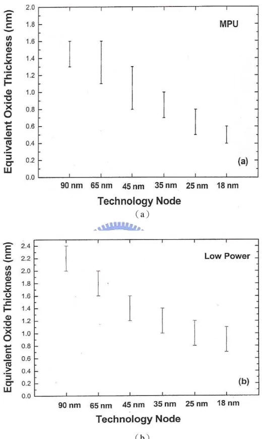
thickness and the shrinkage of the channel length are the simple ways which made the continuous improvement on device performance in the past two decades. However, scaling down of Si device’s dimensions has approached to its fundamental physical limit. Therefore, new materials with higher dielectric constant and novel device structures must be developed. Currently, the CMOS technology node of 90 nm is well developed, According to the International Technology Roadmap for Semiconductors (ITRS) [1], the equivalent oxide thickness (EOT) should be less than 1.6 nm for next generation. Figure 1-1 (a) and (b) depict the shrinking trend of equivalent oxide thickness as a function of technology node for microprocessor and low power devices. Although silicon oxy-nitride (SiON) gate dielectric has replaced SiO2 to achieve 90 nm technology node by its better dielectric integrity and
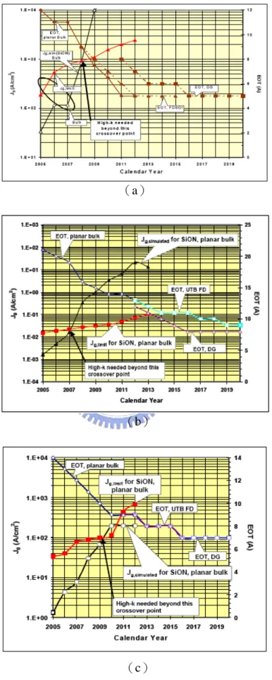
lower stress induced leakage current, the dielectric constant of SiON is not high enough for 65 nm technology node. Besides, as the thickness of SiO2 and SiON is less than 1.2 nm, the
direct tunneling effect will become a very critical issue to overcome. The resulting gate leakage current will not only degrade the device performance but increase the power dissipation. The relation between gate leakage current and EOT is shown in figure 1-2 (a) to (c) where “Jg,limit” is the gate leakage current density limit, and “Jg,simulated” is the
expected value of the gate leakage current density from the simulations. Because of direct tunneling current, the leakage current limit cannot be met with using SiON after 2008 for the high-performance logic transistors. Furthermore, the Jg,simulated curve separates rapidly from
the Jg,limit curve after 2008, indicating that the gate leakage current would become
completely out of specification if SiON were to continue to be used for the gate dielectric after 2008. Therefore, the high dielectric constant (high-k) material which significantly reduces gate leakage for a given EOT is clearly needed by 2008.
Recently, high-k materials such as Al2O3, ZrO2, HfO2 and their silicates [2-15] have been
studied widely. Unfortunately, the dielectric constant of most high-k materials is inversely proportional to their band-gap, as shown in figure 1-3. Although the gate leakage current is suppressed by the thicker physical thickness of high-k materials at same EOT, the narrower band-gap and smaller band offset would enhance Schottky emission of carriers. Furthermore, the trap-assisted tunneling, Frenkel-Poole emission and the hopping effect are the problems remain to be solved. Consequently, there are several issues must be improved before those high-k materials take the place of SiO2 and SiON.
(1) Thin interfacial layer.
(2) Low interface state density ( Dit<1011 eV / cm2 )
(3) Thermodynamic stability in direct contact with substrate.
(4) High energy band-gap with more than 1 eV of conduction band offset to reduce carrier thermal emission.
(5) Low gate leakage current ( JG<1 mA/cm2 at VG=VFB + 1 V for PMOS and VG=
(6) Small hysteresis ( hysteresis<20 mV ) (7) Amorphous phase
(8) Good gate compatibility.
(9) Stable process compatibility, especially for the high temperature dopant activation of source/drain.
(10) Less mobility degradation.
On the other hand, improvements of carrier mobility can be obtained by replacing Si channel with strained Si [16]; however, a major breakthrough may be achieved if the conventional Si substrate is replaced by Ge which has high intrinsic carrier mobility. The hole mobility is four times grater than Si and electron mobility is twice as big as Si. Because of its higher low-field carrier mobility and smaller mobility band-gap for supply voltage scaling, there are many attempts to use Ge as a channel material in high-speed field-effect transistors. However, it still remains several important issues, which we have mentioned above, waiting to be solved.
1-2 Motivation
Recently, high-k materials such as HfO2 [17] and ZrO2 [18] have been under intense
investigation for gate dielectric application into the 65 nm technology node and beyond to replace conventional SiO2 or SiON because of the excessive leakage current and reliability
concerns. However, single oxide high-k dielectrics such as HfO2 and ZrO2 have been reported
to be vulnerable to the diffusion of oxygen, which causes formation of a low-k interfacial layer. The incorporation of both Si and N into HfO2 has attracted considerable interest
because of its several improved features addressing those issues facing binary HfO2,
especially for the increase of crystallization temperature and the suppression of defect states caused by the oxygen vacancies in HfO2 film. According to the report [19], Although HfSiON
with optimized composition ratio remains amorphous state up to 1100°C, the dielectric
constant of HfSiON is decrease to about 10, which is caused by the present of silicon oxide bonds. On the other hand, HfOxNy and ZrOxNy [20] seem to be promising for further
scaling-down of EOT since incorporated nitrogen strengthen the immunity against oxygen diffusion as well as boron penetration [21] without lowering the dielectric constant.
As mentioned above, improvements of carrier mobility can be obtained by replacing Si channel with Ge channel owing to its higher intrinsic electron and hole mobility. Unfortunately, GeO2/Ge exhibits unstable interface, poor electrical properties [22] and may be
too disordered intrinsically [23], so the water–soluble and unstable germanium native oxides have been the main obstacles to Ge application. Consequently, growing high-k dielectric materials becomes a very attractive option to overcome the limitations of GeO2 and provide
alternatives to Si-based microelectronics. In this article, we investigate HfOxNy and ZrOxNy
electrical properties of Ge MOS capacitor.
1-3 Organization of the Thesis
In chapter 2, we first studied the high-k/Ge interface properties and discussed about the thermal stability of high-k/Ge interface. We also found that the interfacial layer has distinct thermochemical properties on Ge and Si substrates. Various material analysis techniques, such as x-ray photoelectron spectroscopy (XPS), high-resolution transmission electron microscopy (HRTEM), secondary ion mass spectroscopy (SIMS) and atomic force microscopy (AFM), were performed to characterize the entire structures and surface morphology.
In chapter 3, we studied the effects of thermal processes in Pt/high-k/Ge gate stack by employing capacitance and conductance measurements. The interface properties and thermal stability of high-k/Ge gate stack which we had discussed helped us to understand the thermal mechanism of Pt/high-k/Ge capacitor.
In chapter 4 and chapter 5, we demonstrated three different kinds of surface pretreatments including CF4 plasma pretreatment, NH3 plasma pretreatment and Si2H6
passivation. These surface pretreatments were applied to solve the issues of Pt/high-k/Ge gate stack, such as hysteresis, thermal stability and frequency dispersion.
(a)
(b)
Fig. 1-1 The equivalent oxide thickness versus generation technology node for (a) microprocessor and (b)low power.
(a)
(b)
(c)
Fig. 1-3 Energy gap versus dielectric constant for SiO2, Si3N4, Al2O3, ZrSiO4, HfSiO4, ZrO2
Chapter 2
The High-k/Ge Interface Properties
2-1 Introduction
There have been extensive studies on several promising high-permittivity (high-k) candidates such as HfO2 [24-25], ZrO2 [26] and Al2O3[27] deposited on Ge because of the
application of its higher low-field carrier mobility; the admirable capacitance properties and transistor performances were continually demonstrated in recent years [28-29]. However, it seems essential to clarify what other advantages and disadvantages of Ge as a replacement of Si. For instance, the thinner lower-permittivity interfacial layer was observed in high-k/Ge system [30], which is beneficial in further scaling the equivalent-oxide-thickness (EOT) below 1 nm, meanwhile, this interfacial layer is very thermodynamically unstable which would degrade the electrical characterization seriously. This finding also implies that fundamental dissimilarities exist between the thermochemical properties of the Ge and Si. Annealing GeO2 at 420°C results in the transformation of GeO2 to GeO, and desorbs as GeO
at higher temperatures. In contrast with SiO2, SiO gets transformed into SiO2 up to 780°C and
decomposes to volatile SiO at higher temperatures [31]. Ge native oxide which is unstable and volatile grows easily on Ge surface when exposed to atmosphere. GeO2 seems to play an
mechanism of high-k/Ge interface and how it affects our electrical characterization.
2-2 Experimental Procedures
(100) p-type Ge and Si wafers were subjected to a cleaning process sequence of deionized (DI) water rinse followed by diluted HF acid solution dipping for three cycles. Two different high-k thin films were then deposited by reactive sputtering chamber at 2 x 10⁻⁷ torr; ZrO2 was deposited in an Ar+O2 ambient [O2/Ar+O2=0.2] with a high-purity Zr target, while
ZrOxNy was deposited in an Ar+N2 ambient [N2/Ar+N2=0.33] with residual oxygen. For
studying the interfacial reaction between the interfacial layer and Zr high-k dielectrics on Ge and Si substrates, we analyzed the effect of N2 post-deposition annealing (PDA) on the
chemical configuration by ex-situ x-ray photoelectron spectroscopy (XPS) using an Al Kα source (1486.6 eV). We also employed high-resolution transmission electron microscopy (HRTEM), secondary ion mass spectroscopy (SIMS) and atomic force microscopy (AFM) to characterize the entire structures and surface morphology.
2-3 Results and Discussion
2-3-1 X-ray photoelectron spectroscopy (XPS) and high-resolution
transmission electron microscopy (HRTEM)
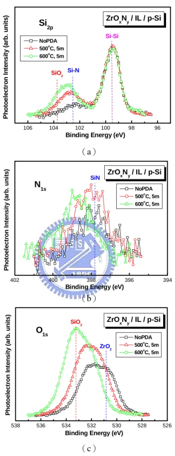
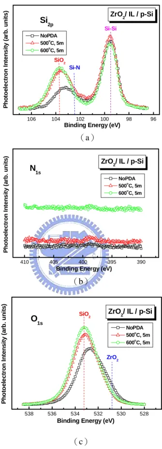
ultra-thin films on Si substrates before and after 500°C or 600°C PDA, respectively. The binding energies of Si-Si, Si-N and SiO2 are 99.5 eV, 102.5 eV and 103.7 eV in Si 2p
spectrum. We observed that as the PDA temperature increases, the intensity of SiO2 increases
clearly, which corresponds to the formation of the interfacial layer as O 1s spectrum. Furthermore, the peak of O 1s spectrum shifts to higher binding energy also indicates the transition from ZrO2 to Zr–silicate.
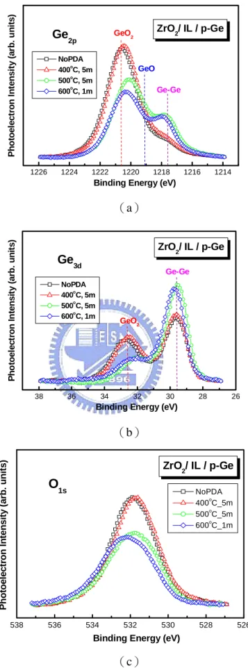
Figure 2-2 (a) to (c) show the core-level spectra of Ge 2p, Ge 3d and O 1s for the ZrOxNy
ultra-thin films on Ge substrates before and after different PDA temperatures. The energies of Ge-Ge, GeO and GeO2 in Ge 2p spectrum are 1217.6 eV, 1219.1 eV and 1220.6 eV,
respectively. Dissimilarly, the intensity of GeO2 is diminished with the increasing PDA
temperatures, which indicates that thermally induced transformation of GeOx (x ≦ 2) into
GeO gaseous species led to severe interfacial layer desorption through the top high-k films. As far as the loss of Ge oxide species is concerned, Ogino and Amemiya proposed two possible reaction mechanisms [32-33] as follows:
2 ( ) ( ) 2 ( ) Ge s +GeO s → GeO v (2.1) 2 1 ( ) ( ) ( ). 2 G e s + O v → G eO v (2.2)
The critical temperature, at which the chemical reduction of GeO2 into volatile GeO takes
place, was reported to range from 350°C to 550°C [34-36]. Higher temperature is believed to be able to accelerate the desorption rate via the mechanism (2.1). Besides, residual oxygen in
an N2 ambient may diffuse through the high-k film and trigger the mechanism (2.2). Therefore,
higher thermal annealing temperature leads to GeOx volatilizes acutely, which is also
evidenced by the reduced intensities of the corresponding O 1s spectra.
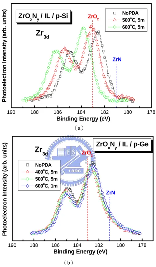
Figure 2-3 (a) and (b) show the Zr 3d core-level spectra of ZrOxNy thin films on Si and
Ge substrate. We observed the spectrum of ZrOxNy/Si gate stacks shifting to higher binding
energy and becoming almost identical after 600°C PDA; this finding indicates that high-temperature annealing tends to convert both the Zr–N and Zr–O bonds into the configuration of Zr–O–Si bond [37-38]. From the O 1s broad spectra in figure 2-1 (c), we confirm this tendency by observing the shifting toward higher binding energy and the increased peak intensity, which is also consistent with the findings of the Si 2p spectra in figure 2-1 (a). Interestingly, there is no evidence of the emergence of interfacial Zr–O–Ge bonding albeit 600°C annealing.
Figure 2-4 (a) to (c) display the core-level spectra of Si 2p, N 1s and O 1s for the ZrO2
ultra-thin films on Si substrates before and after 500°C or 600°C PDA, respectively. Similar to ZrOxNy case, the intensity of SiO2 increases with the PDA temperature increases,
meanwhile the O 1s spectrum also show the transition from ZrO2 to Zr–silicate. Deservedly,
there is no Si-N signal in ZrO2 case.
The spectra in figure 2-5 also suggest that higher annealing temperature would accelerate the desorption rate of GeO2 whatever the high-k film is ZrO2 or ZrOxNy. Figure 2-6 (a) and (b)
show the Zr 3d core-level spectra of ZrO2 thin films on Si and Ge substrate. Without any
thermal process, the interfacial layer tends to be Zr–silicate on Si substrate for the ZrO2 case.
After 600°C PDA, the Zr 3d spectrum shifted to 183.8 eV which is the same value in ZrOxNy
case. In figure 2-6 (b), the subsequent 600°C annealing still can not prompt the occurrence of Zr–germinate, i.e., ZrGeOx: indeed, the spectrum profiles even slightly move backward to
lower binding energy.
The purpose of comparing these two Ge spectra (Ge 2p and Ge 3d) was due to the fact that they have significantly different sampling depths. Through the curve fitting for these two Ge core-levels with mixed Gaussian-Lorentzian line shapes, the amounts of three components (Ge, GeO and GeO2) were extracted, as illustrated in figure 2-7; the inset displays the
HRTEM image of as-deposited ZrO2 thin film, in which an interfacial layer of ca. 22 Å can be
equivocally seen, showing agreement with the estimated thickness of ca. 20 Å by XPS calculation [39]. After annealing at 600°C, the GeOx–contained interfacial layer certainly
revealed acute volatilization, which was also evidenced by the reduced intensity of the corresponding O 1s spectrum.
2-3-2 Secondary ion mass spectroscopy (SIMS) and atomic force microscopy
(AFM)
Ge-N bonds signal was too slight to be detected for XPS, where we verified it in figure 2-8 (a) again, and furthermore increasing annealing temperature would accelerate the breaks of Ge-N bonds. On the contrary, the intensity of Si-N bonds was very strong in figure 2-1, which was corresponded to the result of figure 2-8 (a). In figure 2-8 (b), we found out that Ge diffused into ZrOxNy after 600°C PDA, which was resembled in XPS result and severely degraded the
electrical properties of fabricated high-k/Ge devices.
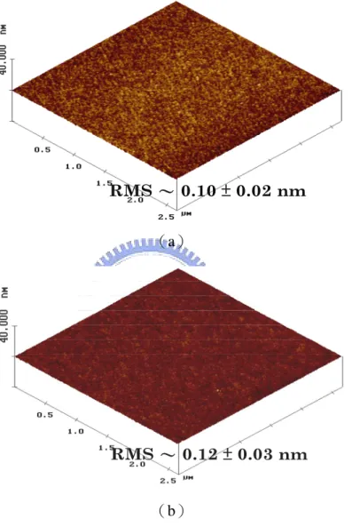
Figure 2-9 and figure 2-10 show the AFM images with different annealing temperatures of Ge substrate. The room-mean-square (RMS) surface roughness was increased with the higher annealing temperatures, indicating that more GeO2 transformed into volatile GeO and
left a lot of small pits and holes on the Ge substrate. Figure 2-11 is the AFM images of ZrOxNy/Si gate stack with and without PDA, and we observed that the surface roughness did
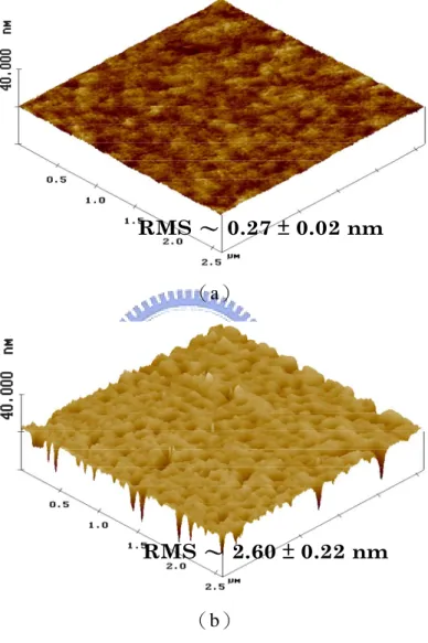
not change apparently even after 600°C PDA. However, the surface morphology of ZrOxNy
overlayer on Ge substrate was clearly damaged after 600°C annealing, as shown in figure 2-12 and 2-13; this in turn possibly created a considerably high defect density and then severely jeopardized the insulating properties of high-k thin film on Ge [40]. Moreover, the surface morphology of ZrO2 overlayer on Ge substrate was damaged seriously after 600°C
annealing, as shown in figure 2-14. We also noticed that the surface roughness of ZrO2/Ge
gate stack was higher than that of ZrOxNy/Ge gate stack, which might due to a great deal of
desorption of GeOx–contained interfacial layer is the possible origin of why we did not
observe the formation of Zr–germinate after high temperature annealing on Ge.
2-4 Summary
In this chapter, we have studied the high-k/Ge interface properties and discussed about the thermal stability of high-k/substrate interface on Ge is not as good as that on Si due to inherent poor quality of Ge native oxide. We found that the interfacial layer has distinct thermochemical properties on these two substrates. High temperature processing aided the interfacial layer growth and the formation of Zr–silicate in ZrOx(Ny)/Si gate stack. On the
contrary, severe interfacial layer volatilization and the inhibition of Zr–germinate were found in ZrOx(Ny)/Ge system; these features are expected to possess a better EOT scalability with
respect to ZrOx(Ny)/Si system. However, the generated localized pits in deposited high-k films
owing to the desorption of the underlying interfacial layer may severely degrade the electrical properties of fabricated high-k/Ge devices.
106 104 102 100 98 96 Si2p ZrOxNy / IL / p-Si NoPDA 500oC, 5m 600oC, 5m P h o to e le c tro n In te n s ity ( a rb . u n its )
Binding Energy (eV)
Si-Si Si-N SiO 2 (a) 402 400 398 396 394 SiN N 1s ZrOxNy / IL / p-Si NoPDA 500oC, 5m 600oC, 5m P h o to e le c tr o n In te n s ity ( a rb . un it s )
Binding Energy (eV)
(b) 538 536 534 532 530 528 526 O 1s ZrOxNy / IL / p-Si NoPDA 500oC, 5m 600oC, 5m Photo elec tron Int ens it y (ar b . uni ts)
Binding Energy (eV) ZrO2
SiO2
(c)
1224 1222 1220 1218 1216 1214 ZrOxNy / IL / p-Ge Ge 2p NoPDA 400o C, 5m 500oC, 5m 600oC, 1m Pho toel ectro n Int ensi ty (ar b . uni ts)
Binding Energy (eV)
GeO2 GeO Ge-Ge (a) 36 34 32 30 28 26 Ge 3d NoPDA 400o C, 5m 500oC, 5m 600oC, 1m P h o toe le c tr o n I n te n s ity (a rb . u n its )
Binding Energy (eV)
GeO 2 Ge-Ge (b) 536 534 532 530 528 ZrOxNy / IL / p-Ge O 1s NoPDA 400oC, 5m 500oC, 5m 600oC, 1m P h o toe le c tr o n Int e n s it y (a rb . un it s)
Binding Energy (eV)
(c)
Fig. 2-2 (a)Ge 2p, (b)Ge 3d and (c)O 1s core-level spectra of ZrOxNy thin films on Ge
190 188 186 184 182 180 178 NoPDA
ZrO
xN
y/ IL / p-Si
ZrO2 500oC, 5mZr
3d ZrN 600oC, 5m Phot oel e c tron I n te ns it y (a rb . u n it s)Binding Energy (eV)
(a) 190 188 186 184 182 180 178 ZrN ZrO 2
ZrO
xN
y/ IL / p-Ge
Zr
3d NoPDA 400oC, 5m 500oC, 5m 600oC, 1m P h ot oe le c tr o n Int e ns it y (a rb . u n its )Binding Energy (eV)
(b)
Fig. 2-3 Zr 3d core-level spectra of ZrOxNy thin films on (a)Si and (b)Ge substrates
106 104 102 100 98 96 ZrO 2/ IL / p-Si Si 2p SiO2 Si-N NoPDA 500oC, 5m 600oC, 5m
Binding Energy (eV)
Si-Si P ho toe lec tr o n In te n s it y (a rb . u n its) (a) 410 405 400 395 390 N 1s ZrO2/ IL / p-Si NoPDA 500o C, 5m 600oC, 5m Pho to e le ctr on I nt e ns it y ( a rb . u n it s)
Binding Energy (eV)
(b) 538 536 534 532 530 528 O 1s ZrO2/ IL / p-Si NoPDA 500o C, 5m 600oC, 5m P h ot o e lec tro n In te n s it y (a rb . un it s )
Binding Energy (eV)
SiO2
ZrO2
(c)
1226 1224 1222 1220 1218 1216 1214 Ge 2p ZrO2/ IL / p-Ge NoPDA 400o C, 5m 500oC, 5m 600o C, 1m P h ot o e le c tr o n In te n s ity ( a rb . un it s )
Binding Energy (eV)
GeO2 GeO Ge-Ge (a) ZrO2/ IL / p-Ge GeO2 Ge-Ge Ge 3d NoPDA 400o C, 5m 500oC, 5m 600oC, 1m P h o toel ec tron In tensit y (arb . unit s)
Binding Energy (eV)
38 36 34 32 30 28 26 (b) 538 536 534 532 530 528 526 O 1s ZrO2/ IL / p-Ge NoPDA 400oC_5m 500oC_5m 600o C_1m Ph otoel e c tr o n I n te nsi ty ( a rb. un it s )
Binding Energy (eV)
(c)
substrates before and after different PDA temperatures. 190 188 186 184 182 180
Zr
3dZrO
2/ IL / p-Si
NoPDA 500oC, 5m 600oC, 5m P h o toe le c tron In te ns ity (a rb . un its )Binding Energy (eV)
ZrO2 ZrN (a) 190 188 186 184 182 180 178
Zr
3dZrO
2/ IL / p-Ge
NoPDA 400oC, 5m 500oC, 5m 600oC, 1m Phot oe lect ron I n te nsit y ( a rb . unit s )Binding Energy (eV)
ZrO
2
ZrN
(b)
Fig. 2-6 Zr 3d core-level spectra of ZrO2 thin films on (a)Si and (b)Ge substrates before
Annealing Conditions
ZrON
ZrO
2Annealing Conditions
ZrON
ZrO
2Fig. 2-7 The ratio of GeOx to Ge substrate versus annealing conditions for ZrOxNy/Ge and
ZrO2/Ge gate stacks. Inset: cross-sectional TEM image of ZrO2/Ge gate stacks
0 3 6 9 12 15 1019 1020 1021 1022 ZrON / IL substrate Ap pr oxi m a te N A to m ic Per c ent ag e (% ) Ge (600oC PDA) Ge (as-dep.) Si (as-dep.) ZrON / IL / sub. N At o m ic C o n c e n tra ti on ( a to ms /c c) Depth (nm) 10-1 100 101 (a) 0 2 4 6 8 10 101 102 103 104 105 106 A p p ro x im at e N A to m ic P e rc e n ta g e (% ) Zr, G e , O S e c o n d a ry Io n In te ns it y ( c ts /s e c )
N
ZrON IL Ge sub.Dash line: as-dep. Solid line: 600oC PDA
Zr
ZrON / IL / GeO
Ge
Depth (nm) 10-2 10-1 100 101 102 (b)Fig. 2-8 The SIMS depth profiles for ZrOxNy thin films on (a)Si and Ge substrates and
RMS ~ 0.38 ± 0.02 nm RMS ~ 0.38 ± 0.02 nm (a) RMS ~ 0.38 ± 0.03 nm RMS ~ 0.38 ± 0.03 nm (b) RMS ~ 0.55 ± 0.05 nm RMS ~ 0.55 ± 0.05 nm (c)
Fig. 2-9 The AFM images of Ge substrate with (a)no annealing, (b)400°C annealing for 5 min and (c)500°C annealing for 5 min.
RMS ~ 0.65 ± 0.03 nm RMS ~ 0.65 ± 0.03 nm (a) RMS ~ 2.21 ± 0.16 nm RMS ~ 2.21 ± 0.16 nm (b)
Fig. 2-10 The AFM images of Ge substrate with (a)600°C annealing for 1 min and (b) 600°C annealing for 5 min.
RMS ~ 0.10 ± 0.02 nm RMS ~ 0.10 ± 0.02 nm (a) RMS ~ 0.12 ± 0.03 nm RMS ~ 0.12 ± 0.03 nm (b)
Fig. 2-11 The AFM images of ZrOxNy/Si gate stack with (a)as-deposited and (b)600°C
RMS ~ 0.21 ± 0.02 nm RMS ~ 0.21 ± 0.02 nm (a) RMS ~ 0.25 ± 0.02 nm RMS ~ 0.25 ± 0.02 nm (b)
Fig. 2-12 The AFM images of ZrOxNy/Ge gate stack with (a)as-deposited and (b)500°C
RMS ~ 0.27 ± 0.02 nm RMS ~ 0.27 ± 0.02 nm (a) RMS ~ 2.60 ± 0.22 nm RMS ~ 2.60 ± 0.22 nm (b)
Fig. 2-13 The AFM images of ZrOxNy/Ge gate stack with (a)600°C PDA for 1 min and
RMS ~ 0.30 ± 0.04 nm RMS ~ 0.30 ± 0.04 nm (a) RMS ~ 3.03 ± 0.11 nm RMS ~ 3.03 ± 0.11 nm (b)
Fig. 2-14 The AFM images of ZrO2/Ge gate stack with (a)600°C PDA for 1 min and (b)
Chapter 3
Post Dielectric/Metal Annealing
3-1 Introduction
Silicon has been used in CMOS technology for decades due to better qualities of its native oxide such as low interface state density and good thermal stability. But, with further downscaling device dimensions and the shrinkage of gate oxide thickness to nanometer range, the leakage current density of SiO2 is too large to be accepted. Recently, Ge-channel devices
which including bulk Ge [41-42] and strained Ge [43] with the integration of high-k gate dielectrics have gained considerable research interest. Some materials which have high dielectric constant are being introduced to suppress excessive leakage concern with a thicker physical thickness while still maintaining the capacitance equivalent thickness (CET) of the scaled devices. Up to the present, HfO2, ZrO2 and their oxynitride are the uppermost
candidates among all potential high-k dielectrics. Both Si and Ge MOSFETs with high-k gate dielectrics have shown some promising performances [44-45]. Our work presents the electrical characteristics of HfOxNy thin films deposited on bulk Ge substrate, and the impact
3-2 Experimental Procedures
MOS capacitors were fabricated on (100) oriented n-type Ge substrates which were doped with Sb having a resistivity of 8–12 Ω·cm. Deionized (DI) water rinse followed by diluted HF acid solution dipping for three cycles in order to remove Ge native oxide. Subsequently, HfOxNy thin films were first deposited through reactive sputtering in an Ar+N2
[N2/Ar+N2=0.33] ambient with a pure Hf target, and then annealing in N2 gas with residual
oxygen. Next, a 1000 Å layer of platinum (Pt) dot was deposited using electron beam evaporation through a shadow mask. Finally, Al was deposited on the backside of Ge wafer to reduce the contact and series resistances. For comparison, as-deposited HfOxNy films were
annealed at the temperatures of 500°C and 600°C, respectively; same annealing conditions
were employed after metallization for evaluating thermal stability of the Pt/high-k/Ge structures. The capacitance−voltage (C−V) and conductance−voltage (G–V) curves were measured using an HP4284 LCR meter, while the current−voltage (I−V) characteristics were
measured using a Keithley 4200 semiconductor analyzer system. The series resistance was extracted and then applied as a correction to the measured capacitance and conductance. The interface state density (Dit) at the midgap is determined from G–V characteristics by using
3-3 Results and Discussion
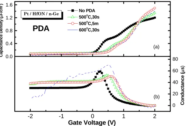
Figure 3-1 (a) and (b) display typical 100-kHz C–V and G–V characteristics of the HfOxNy/Ge capacitors before and after post dielectric annealing (PDA), the sweep direction of
all curves presented in our figures are from Vg = +2 V to Vg = -2 V; that is from strong
accumulation to strong inversion. The CET estimated at Vg = +2 V in C–V curves was ca. 28
Å for as-deposited samples and decreased to ca. 25 Å and ca. 22 Å after annealing at 500°C
for 30 sec and 5 min, respectively. The further CET scaling could be achieved by extending annealing duration or increasing the annealing temperatures. Consequently, we believe that annealing processes not only made the densification of HfOxNy film but also the shrinkage of
interfacial layer, showing agreement with the observation in chapter 2. Furthermore, the G–V characteristics obviously revealed the energy loss peak, corresponding to the hump observed in the depletion region in C–V curves, indicating the existence of fast interface states at the HfOxNy/Ge interface. Another noteworthy feature was that the measured conductance in
inversion showed gate-bias independence; this phenomenon is rare for traditional Si MOS capacitors. Figure 3-2 shows the C–V and G–V characteristics of the HfOxNy/Si capacitor at
100-kHz, the equivalent parallel conductance goes through a peak in weak inversion and immediately drops to a very low value in strong inversion. In contrast with HfOxNy/Ge
capacitors case, the gate-bias independent conductance observed in inversion reflects the fact that the generation and recombination of minority carriers indeed contributes an energy loss in
inversion and competes with interface state loss in depletion.
Figure 3-3 (a) and (b) display typical 100-kHz C–V and G–V characteristics of the HfOxNy/Ge capacitors before and after post metal annealing (PMA), respectively.The lowest
CET value of ca. 23 Å was achieved after PMA at 500°C for 5 min. In comparison with PDA
processes, the PMA process apparently relieves the hump emerged in as-deposited sample, as evidenced by vanishing conductance peak in G–V curves. Interestingly, PMA samples depict contrasting behavior in inversion as compared to PDA ones; the measured capacitance and conductance simultaneously raise with increasing PMA temperature and time, which is a typical characteristic of the increase of bulk traps presumably caused by introducing Pt atoms during high temperature annealing, as shown in figure 3-4. Except for the contribution to more bulk traps loss, the bulky defects with energy levels near midgap in Ge, which are also responsible for the supply of minority carriers to the inversion layer, incur the onset of low-frequency-like C–V characteristic, even in the kHz range.
Figure 3-5 analyzed Dit with different kinds of annealing conditions. The as-deposited
HfOxNy/Ge sample revealed a large value of the Dit of ca. 4 x 1012 cm-2eV-1, which probably
associated with poor quality of the interfacial layer. However, the Dit reduced to ca. 2.5 x 10¹²
and ca. 1 x 1012 cm-2eV-1 for PDA and PMA samples, respectively. In order to figure out the charge trapping effect and the improvement of interface quality during annealing, we discussed them together with the examination of the Vfb in figure 3-6. The Vfb of as-deposited
sample was ca. 0.35 V lower than the ideal work-function difference which is ca. 0.9 eV between Pt electrode and n-Ge substrate, implying that substantial positive charges have been introduced in the gate dielectric/interfacial layer during the post-process. With increasing the annealing temperature, the value of Vfb undergoes a positive shift, indicating that positive
charges have been remedied by high temperature annealing, otherwise, the diffusion of Ge or the volatilization of GeO would generate additional negative charges and led to the charge neutralization.
The volatilization of GeO not only made the shrinkage of interfacial layer but also created the leakage-paths in the gate dielectric, as shown in figure 3-7, the gate leakage current increased with the higher annealing temperature, which was coincided with the amount of GeO volatilization. Figure 3-8 depict the hysteresis of Pt/high-k/Ge capacitors which hysteresis was about 600 to 700 mV except PMA at 600°C for 5 min. The large gate leakage current resulted in the abrupt reduction of hysteresis of PMA 600°C sample. In
contrast with Pt/high-k/Si capacitors, the negligible hysteresis was below 50mV. The detailed analysis of hysteresis will be discussed in next chapter.
3-4 Summary
In this chapter, we found that the PDA process did not multiply the pre-existing bulk traps in Ge substrate, which was conformed by corresponding G–V results, whereas the PMA
process increased them, and thus presented low-frequency-like behavior in high-frequency C–V curves. Furthermore, both annealing processes were found to annihilate the amount of Dit and shrink the CET, but these thermal processed increased the gate leakage current at the
-2 -1 0 1 2 C o nd uc ta nc e ( μs )
PDA
No PDA 500oC,30s 500oC,5m 600oC,30s C a p a c it a nc e D e ns it y ( μF/cm 2 )Gate Voltage (V)
0 20 40 60 80 (b) (a) 0.0 0.4 0.8 1.2 1.6 Pt / HfON / n-GeFig. 3-1 Typical 100-kHz(a)C–V and (b)G–V curves of Pt/HfOxNy/n-Ge capacitors
before and after PDA, respectively.
-1 0 1 2 3 0 200 400 600
Gate Voltage (V)
C
a
pa
ci
ta
nc
e (
pF)
Co n d u c ta n c e (μ s) 0 10 20 30 40Pt / HfON / n-Si
-2 -1 0 1 2
Gate Voltage (V)
C a p a c it a nc e De ns it y ( μF/ c m 2 ) 0 40 80 120 (b) C o ndu ct ance ( μs ) 0.0 0.4 0.8 1.2 1.6 (a) No PDA 500oC,30s 500oC,5m 600oC,30sPMA
Pt / HfON / n-GeFig. 3-3 Typical 100-kHz(a)C–V and (b)G–V curves of Pt/HfOxNy/n-Ge capacitors
before and after PMA, respectively.
0 20 40 60 80 100 120 140 160 180 200
Io
n
In
te
n
s
it
y
Depth (nm)
Pt / HfON / n-Ge
Ge
Pt
NoPDA PDA PMAPt diffusion
0 20 40 60 80 100 120 140 160 180 200Io
n
In
te
n
s
it
y
Depth (nm)
Pt / HfON / n-Ge
Ge
Pt
NoPDA PDA PMAPt diffusion
2 4 6 8 10
as-dep.
500oC,30s 500oC,5m 600oC,30sD
it( 10
12/ cm
2eV
)
PDA
PMA
Fig. 3-5 The Dit of as-deposited Pt/high-k/Ge capacitors and annealed ones.
0.2
0.4
0.6
0.8
V
fb(v
o
lts
)
PDA
PMA
as-dep.
500
oC,30s
500
oC,5m
600
oC,30s
Fig. 3-6 The flat-band voltage of Pt/high-k/Ge capacitors for as-deposited and annealed ones.
10-7 10-6 1x10⁻⁵ 1x10⁻⁴ 10-3 10-2 10-1 100
as-dep.
500
oC,5m
600
oC,30s
PDA
PMA
Le aka g e C u rr e n t D e ns it y @ V fb + 1V (A /cm 2 )500
oC,30s
Fig. 3-7 The gate leakage current density of Pt/high-k/Ge capacitors for as-deposited and annealed ones.
300 400 500 600 700 800 900 1000
H
y
s
ter
es
is (
m
V
)
600oC,30s 500oC,5m 500oC,30sas-dep.
PDA
PMA
Chapter 4
CF
4
and NH
3
Plasma Pretreatment
4-1 Introduction
Ge has recently retrieved enormous attentions due to its higher hole and electron mobility than Si (4x for hole and 2x for electron). Unfortunately, GeO2 and GeO are
thermodynamically unstable and soluble to water, which retard the development of high-performance Ge-MOSFET. Therefore, looking for high-k materials such as HfO2 or
ZrO2 to be substitute gate dielectric is in demand. The incorporation of N into both HfO2 and
ZrO2 has attracted considerable interest because of its several improved features addressing
those issues facing binary HfO2, especially for the increase of crystallization temperature and
the suppression of defect states caused by the oxygen vacancies in HfO2 film. Moreover,
HfOxNy and ZrOxNy seem to be promising for further scaling-down of EOT since
incorporated nitrogen strengthen the immunity against oxygen diffusion as well as boron penetration without lowering the dielectric constant. However, it was reported that before or during the post-process, the Ge surface would be oxidized to form GeOx and lead to the
degradation of device performance [47-48]. The methods to reduce those excessive GeOx
growths and improve the electrical performance are the purpose of this chapter, which included CF4 plasma and NH3 plasma surface pretreatments.
4-2 Experimental Procedures
MOS capacitors were fabricated on (100) oriented n-type Ge substrates which were doped with Sb having a resistivity of 8–12 Ω·cm. Deionized (DI) water rinse followed by diluted HF acid solution dipping for three cycles. After clean process, CF4 or NH3 plasma was
demonstrated on Ge surface in plasma-enhanced chemical vapor deposition (PECVD). Subsequently, HfOxNy or ZrOxNy thin films were first deposited through reactive sputtering in
an Ar+N2 [N2/Ar+N2=0.33] ambient with pure Hf or Zr target and the sputtering power was
150 W at the chamber pressure of 7.6 mTorr, and then annealing in N2 gas with residual
oxygen. Next, a 1000 Å layer of platinum (Pt) dot was deposited using electron beam evaporation through a shadow mask, subsequently, annealing in N2 gas with residual oxygen
at 400°C for 30 sec to make the densification of our metal gate. Finally, Al was deposited on the backside of Ge wafer to reduce the contact and series resistances. For comparison, the Si substrate was also demonstrated by same processes.
The capacitance−voltage (C−V) and conductance−voltage (G–V) curves were measured using an HP4284 LCR meter, while the current−voltage (I−V) characteristics were measured using a Keithley 4200 semiconductor analyzer system. We analyzed the effect of NH3 plasma
pretreatment on the chemical configuration by ex-situ XPS using an Al Kα source (1486.6 eV). We also employed atomic force microscopy (AFM) to characterize the surface morphology of CF4 plasma samples.
4-3 Results and Discussion
4-3-1 The hysteresis of Pt/ZrO
xN
y/Ge gate stack
Figure 4-1 displays the typical 1-MHz C–V curves of Pt/ZrOxNy/n-Ge capacitor without
any surface pretreatment, which exhibits ca. 650 mV of hysteresis width. In contrast with Pt/ZrOxNy/n-Si capacitor shown in figure 4-2, the negligible hysteresis is only ca. 50mV, and
the frequency dispersion effect of Pt/ZrOxNy/Si gate stack is very slight. It stands to reason
that the issues of hysteresis and frequency dispersion existed in the Pt/ZrOxNy/n-Ge gate stack
have no relationship with our ZrOxNy gate dielectric and Pt metal gate.
In order to discover the origin of hysteresis of Pt/ZrOxNy/n-Ge capacitor, first, we
fastened down the gate bias (Vg) at 0 V in inversion region and then swept from 0 V to
different accumulation bias (1 V, 1.2 V, 1.4 V, 1.6 V, 1.8 V and 2 V, respectively). Oppositely, we fastened down the Vg at 1 V in accumulation region and swept from 1 V to
different inversion bias (0 V, -1.2 V, -1.4 V, -1.6 V, -1.8 V and -2 V, respectively). All these results are shown in figure 4-3. Obviously, the sweep direction from Vg = +1 V to strong
inversion resulted in the presence of hysteresis effect, whereas the sweep direction from Vg =
0 V to strong accumulation did not. Consequently, the hysteresis of Pt/ZrOxNy/Ge capacitor
might result from the hole trapping effect and corresponding trapping mechanism was deduced in figure 4-4 and figure 4-5. When the capacitor was biased at strong inversion, the holes near valence band of Ge substrate tunneled from Ge surface to interfacial layer and
trapped at the inner-interface. On the other hand, when the capacitor was biased at strong accumulation, the electrons near conduction band of Ge substrate tunneled through the interfacial layer and gate dielectric ZrOxNy without being trapped at the inner-interface, thus
contributing to the gate leakage current.
Figure 4-6 shows the gate leakage current of Pt/ZrOxNy/Ge capacitor, the flat-band
voltage is ca. 0.35 V with respect to the C-V curve (dashed line), the gate leakage current density is ca. 9 x 10⁻⁷ A·cm-2 and ca. 1 x 10⁻⁵ A·cm-2 at Vfb - 1 V and Vfb + 1 V, respectively.
Apparently, the gate leakage current at strong accumulation condition is greater than the leakage current at strong inversion condition, which is coincided with the result of energy-band diagrams in figure 4-4 and figure 4-5.
4-3-2 CF
4plasma pretreatment
Figure 4-7 displays the 1-MHz C–V curves of Pt/ZrOxNy/n-Ge capacitors with and
without CF4 plasma pretreatment. After CF4 plasma pretreatment, the hysteresis width of
Pt/ZrOxNy/n-Ge capacitors increased from 650 mV to 950 mV, whereas the 3 watt CF4 plasma
was ineffective to Pt/ZrOxNy/n-Si gate stack. As shown in figure 4-8, the C-V curves of
Pt/ZrOxNy/n-Si capacitors remained identical whatever CF4 plasma was demonstrated or not,
which indicated that the power of CF4 plasma was too small to react with Si surface. It also
density at Vfb + 1 V of Pt/ZrOxNy/Si capacitors was all ca. 10-6 A·cm-2 for 0 watt, 2 watt and 3
watt CF4 plasma pretreatment. In contrast with Pt/ZrOxNy/Ge gate stacks, the gate leakage
current increased with the uplifting CF4 plasma power.
The enlargement of hysteresis phenomnomn after CF4 plasma pretreatment was
examined by the previous method we used; figure 4-10 demonstrated the 1-MHz C–V curves of Pt/ZrOxNy/n-Ge capacitor with CF4 plasma treatment. First, we swept the gate bias from 0
V to 1 V, 1.2 V, 1.4 V, 1.6 V, 1.8 V and 2 V, respectively. And then the gate bias was swept from 1 V to 0 V, -1.2 V, -1.4 V, -1.6 V, -1.8 V and -2 V, respectively. Interestingly, the curves of sweep direction from Vg = 0 V to strong accumulation region began to shift
positively and curves of sweep direction from Vg = 1 V to strong inversion region moved even
more manifestly, which implied that CF4 plasma pretreatment induced trapping centers not
only near conduction band but also valence band of Ge.
Figure 4-11 shows the AFM images of Ge substrates before and after CF4 plasma
pretreatment, the room-mean-square (RMS) surface roughness is increased from 0.35 nm to 0.46 nm, which probably incurred the larger gate leakage current of Pt/ZrOxNy/n-Ge
capacitors in figure 4-9. However, 3 watt CF4 plasma was ineffectual to change the surface
4-3-3 NH
3plasma pretreatment
High-frequency (1-MHz) C–V curves of Pt/HfOxNy/n-Ge capacitors with and without
NH3 plasma pretreatment was shown in figure 4-13. After NH3 plasma pretreatment, the
hysteresis width of Pt/HfOxNy/n-Ge capacitors was reduced from 650 mV to 400 mV. On the
contrary, the hysteresis width of Pt/HfOxNy/n-Si capacitors remained ca. 30 mV, which was
independent of applied NH3 plasma, implying that the power of NH3 plasma was not enough
to nitride the Si surface.
Figure 4-15 (a) and (b) show the core-level spectra of Ge 2p and Ge 3p for the HfOxNy/n-Ge gate stacks. Manifestly, NH3 plasma pretreatment suppressed the growth of
GeOx, which restrained the electrons and holes from trapping at HfOxNy/IL interface and
diminished the hysteresis width of Pt/HfOxNy/n-Ge capacitors.
As we discussed in chapter 2 and chapter 3, the volatilization of GeO would damage the gate dielectric and generate leakage-paths in it especially after high-temperature annealing. However, the NH3 pretreatment samples reduced the gate leakage current by two orders of
magnitude after PDA at 600°C for 30 sec, as shown in figure 4-16, which was attributed to the nitrided-surface and leading to a small amount of GeO volatilization.
Figure 4-17 displays the Dit of as-deposited Pt/high-k/Ge capacitors before and after
surface pretreatment, the Dit was determined from G–V characteristics at the frequency of
indicated an increment in charge traps possible at the interface of high-k/IL. On the other hand, the NH3 plasma pretreatment compressed the hysteresis width implied a reduction in
charge traps at the interface of high-k/IL, which was likely related to less native oxide of nitrided samples.
4-4 Summary
In this chapter, we found that the hysteresis of both Pt/ZrOxNy/n-Ge and Pt/HfOxNy/n-Ge
(not shown) capacitors was due to the trapping centers at high-k/IL interface near the valence band of Ge. The CF4 plasma pretreatment enlarged the gate leakage current and hysteresis
width of Pt/high-k/Ge capacitors, which were possibly due to damage Ge surface and the increment of Dit. On the other hand, the NH3 plasma pretreatment compressed the hysteresis
width, which was likely related with less GeOx and Dit. Moreover, the nitridation process
improved the thermal stability of Pt/high-k/Ge capacitors by restraining the formation of GeOx and their volatilization.