Spatial redistribution of the optical field intensity in inverted polymer solar cells
Fang-Chung Chen, Jyh-Lih Wu, and Yi Hung
Citation: Applied Physics Letters 96, 193304 (2010); doi: 10.1063/1.3430060 View online: http://dx.doi.org/10.1063/1.3430060
View Table of Contents: http://scitation.aip.org/content/aip/journal/apl/96/19?ver=pdfcov Published by the AIP Publishing
Articles you may be interested in
Performance improvement of inverted polymer solar cells by doping Au nanoparticles into TiO2 cathode buffer layer
Appl. Phys. Lett. 103, 233303 (2013); 10.1063/1.4840319
Increased efficiency of low band gap polymer solar cells at elevated temperature and its origins Appl. Phys. Lett. 99, 133302 (2011); 10.1063/1.3643450
Improved power conversion efficiency of InP solar cells using organic window layers Appl. Phys. Lett. 98, 053504 (2011); 10.1063/1.3549692
Organic solar cells with a multicharge separation structure consisting of a thin rubrene fluorescent dye for open circuit voltage enhancement
Appl. Phys. Lett. 98, 023301 (2011); 10.1063/1.3535603
Efficient multilayer organic solar cells using the optical interference peak Appl. Phys. Lett. 93, 043307 (2008); 10.1063/1.2962986
This article is copyrighted as indicated in the article. Reuse of AIP content is subject to the terms at: http://scitation.aip.org/termsconditions. Downloaded to IP: 140.113.38.11 On: Wed, 30 Apr 2014 10:22:33
Spatial redistribution of the optical field intensity in inverted polymer
solar cells
Fang-Chung Chen,1,2,a兲Jyh-Lih Wu,1,3and Yi Hung1,2
1Department of Photonics, National Chiao Tung University, Hsinchu 30010, Taiwan 2Display Institute, National Chiao Tung University, Hsinchu 30010, Taiwan
3Institute of Electro-Optical Engineering, National Chiao Tung University, Hsinchu 30010, Taiwan
共Received 7 January 2010; accepted 25 April 2010; published online 14 May 2010兲
We have used indium tin oxide 共ITO兲, a transparent conducting oxide, as an optical spacer to improve the performance of inverted polymer solar cells. The optical interference effect resulted in spatial redistribution of the optical field in the devices. Although the degree of light absorption in inverted cells was not increased, the resulting favorable distribution of photogenerated excitons probably decreased the level of exciton quenching near the electrodes. As a result, the introduction of the ITO optical spacer at an appropriate thickness increased the short-circuit current density and the overall power conversion efficiency. © 2010 American Institute of Physics. 关doi:10.1063/1.3430060兴
Organic photovoltaic devices 共OPVs兲 are attracting in-creasing attention because of their light weight, low cost, fabrication at low temperature, semitransparency, and mechanical flexibility. Recently, polymer/fullerene bulk-heterojunction solar cells have dominated the burgeoning field of OPVs; the power conversion efficiencies共PCEs兲 of these devices have reached as high as 6%.1–4 In particular, some OPVs featuring an inverted device architecture— eliminating the acidic poly共3,4-ethylenedioxythiophene兲: poly共styrene sulfonate兲 anodic buffer layer and the air sensi-tive metals—have exhibited prolonged device lifetimes.5–8 Accordingly, much effort is being exerted in the quest for high-performance inverted OPVs.6–10One feasible approach toward highly efficient devices is the exploitation of light trapping techniques.11–13 Among them, the incorporation of an optical spacer, which redistributes the optical field spa-tially in the active layer, can improve the PCEs of OPVs having regular device architectures.4,14–16 Nevertheless, rel-evant studies of the optical interference effect in inverted OPVs remain rare so far.17
In this study, we explored the effect of incorporating indium tin oxide 共ITO兲 as an optical spacer on the perfor-mance of inverted OPV devices. The prerequisites for a func-tional optical spacer in OPVs include high electrical conduc-tivity共to avoid the increased device resistance兲, high optical transparency, and alignment of the energy levels of the in-volved layers. ITO appears to be a suitable candidate for use as an optical spacer between the organic active layer and the top electrode in the inverted OPVs—except that its work function 共approximately 4.7 eV兲 共Ref. 18兲 somehow
mis-aligns with the highest occupied molecular orbital of poly共3-hexylthiophene兲 共approximately 5.2 eV兲.18 This problem could be easily solved, however, by incorporating high-work-function molybdenum trioxide 共MoO3; approximately
5.3 eV兲 共Ref. 18兲 as an interlayer to match the energy
levels.10,18Our results of this MoO3/ITO “bilayer structure”
revealed that the introduction of the ITO optical spacer no-tably enhanced the photocurrent, thereby increasing the
over-all device efficiency. More interestingly, as will be shown in this study, the optical interference effect, induced by the presence of the ITO optical spacer, remained beneficial to the device performance of inverted OPVs when optimizing the thickness of the active layer.
To fabricate the inverted OPV device, an interfacial layer of cesium carbonate 共Cs2CO3; 99.995% purity from Aldrich兲 was spin-coated onto the ITO-coated glass substrate from a solution in 2-ethoxyethanol 共2 mg/ml兲, followed by thermal annealing at 150 ° C for 15 min.7The photoactive layer was spin-coated on top of the Cs2CO3 from a blend of poly共3-hexylthiophene兲 共P3HT; Rieke Metals兲 and 关6,6兴-phenyl-C61-butyric acid methyl ester 共PCBM;
Ameri-can Dye Source兲 dissolved in 1,2-dichlorobenzene 共17 mg/ ml: 17 mg/ml兲. After solvent annealing,19
the dried film was thermally annealed at 110 ° C for 15 min; the resulting film was approximately 180 nm thick. We note that the thickness of the active layer has been optimized experimentally. To complete the device, 20 nm thick MoO3 and 150 nm thick
Ag layers were sequentially deposited through thermal evaporation to function as the hole-collection contact. Here, Ag was used as the anodic electrode because of its high reflectance and conductivity. ITO layers of various thick-nesses were inserted between the MoO3 and Ag layers through rf sputtering to function as optical spacers. The de-vice area, defined through a shadow mask, was 0.12 cm2.
All of the completed devices were thermally postannealed at 140 ° C for 5 min in a glovebox. The inset of Fig. 1共a兲 pro-vides a schematic representation of the device architecture. The current density-voltage 共J-V兲 characteristics of the de-vices were measured using a Keithley 2400 source-measure unit. The photocurrent was obtained under air mass 1.5 glo-bal 共AM 1.5G兲 illumination from a 150 W Thermal Oriel solar simulator. The illumination intensity was calibrated us-ing a standard Si photodiode equipped with a KG-5 filter 共Hamamatsu, Inc.兲.20
Optical modeling was performed using the optical transfer matrix formalism共TMF兲 approach.21The optical constants, including the refractive index 共n兲 and ex-tinction coefficient 共k兲, of each layer in the device structure were obtained using the ellipsometry method. The film thick-ness of each layer was determined using atomic force
mi-a兲Author to whom correspondence should be addressed. Electronic mail: [email protected].
APPLIED PHYSICS LETTERS 96, 193304共2010兲
0003-6951/2010/96共19兲/193304/3/$30.00 96, 193304-1 © 2010 American Institute of Physics This article is copyrighted as indicated in the article. Reuse of AIP content is subject to the terms at: http://scitation.aip.org/termsconditions. Downloaded to IP:
croscopy共AFM兲 and also confirmed employing the ellipsom-etry measurement.
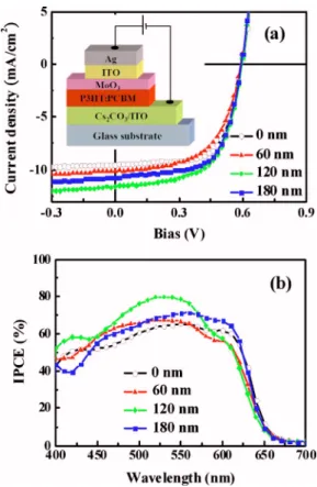
Figure1共a兲displays the J-V characteristics, recorded un-der 100 mW cm−2illumination共AM 1.5G兲, of OPV devices incorporating ITO optical spacers of various thicknesses 共Table I兲. The reference device possessing the structure
ITO/Cs2CO3/P3HT:PCBM/MoO3/Ag exhibited an open-circuit voltage共Voc兲 of 0.59 V, a short-circuit current 共Jsc兲 of
9.54 mA cm−2, and a fill factor 共FF兲 of 0.67, yielding an overall device PCE of 3.76%. The typical photovoltaic char-acteristics suggested that functional 共Ohmic兲 contacts were formed at both contacts共ITO/Cs2CO3 and MoO3/Ag兲. Note that Cs2CO3 共Refs. 5 and 7兲 and MoO3 共Refs. 10 and 18兲
have been proposed to act as functional electron-selective and hole-selective layers, respectively, for efficient charge collection in OPVs. To further benefit from the optical inter-ference effect, we inserted ITO layers of various thicknesses 共60, 120, and 180 nm兲 between the MoO3 and Ag layers. In
each case, the value of Voc remained at 0.59 V. In contrast,
the value of Jscwas strongly dependent on the ITO thickness:
its optimum value occurred for an ITO thickness of 120 nm. Moreover, the FF decreased slightly after inserting the ITO optical spacers, presumably because of increased device series resistance arising from the presence of ITO22 and/or possible sputtering damage. Such disadvanta-geous effects could, however, be overwhelmed through the incorporation of an optical spacer of a suitable thickness. The device incorporating the 120 nm thick ITO optical spacer achieved an excellent PCE of 4.20% 共Voc= 0.59 V ; Jsc
= 11.49 mA cm−2; FF= 0.62兲. In general, the expected
per-formance enhancement from the optical interference effect is negated when the active layer is sufficiently thick.14,17,23 Sur-prisingly, the inverted OPVs fabricated in this study could still benefit from the introduction of an ITO optical spacer while the thickness of the active layer was optimized.
We also compared the spectral response for devices with and without optical spacers. The incident photon-to-electron conversion efficiency 共IPCE兲 is measured to determine the spectral response of OPVs. Figure 1共b兲 displays the IPCE curves for these devices. One can see that both the shape and the maximum position of spectral response changed signifi-cantly after inserting an ITO optical spacer, presumably be-cause of the optical interference effect be-caused by the ITO optical spacer.
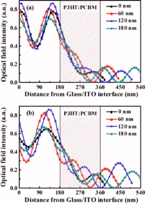
To understand the mechanism responsible for the in-creased values of Jsc, we also numerically investigated the
optical interference effect of incorporating an optical spacer in OPVs through TMF optical modeling, which has been used widely to investigate the optical behavior of OPV devices.14,17,24 The optical field intensity 共兩E共z兲兩2兲 at any
given position in the device can be calculated from the opti-cal constants共n and k兲 and the depth of each layer. Figure2
displays the effect of the optical spacers on the calculated distribution profiles of optical field intensity in the device at given wavelengths共兲 of 500 and 550 nm. The spatial dis-tribution of the optical field intensity was strongly dependent on the thickness of the optical spacer.
For quantitative analysis, therefore, we further calculated the distribution profiles for the exciton generation rate G共z兲 inside the active layer via the energy dissipation rate 共Fig.
3兲.13,24 Figure 3 reveals that the incorporation of an ITO spacer effectively tailored the distribution of photogenerated excitons. After incorporating a 120 nm thick ITO optical spacer, the values of G共z兲 increased within the depth range from 60 to 120 nm but decreased near both organic/electrode contacts. We suspect that the dramatic change in the distri-bution profile of G共z兲 contributed to the enhanced photocur-rent.
Previously, Moulé and Meerholz25 suggested that the photocurrent decreased when the light intensity in the prox-imity of the organic/electrode interface increased due to the FIG. 1.共Color online兲 共a兲 J-V characteristics, recorded under 100 mW cm−2
illumination共AM 1.5G兲, of polymer solar cells incorporating ITO optical spacers of various thicknesses. Inset: device architecture of OPVs incorpo-rating an ITO optical spacer.共b兲 IPCE curves of polymer solar cells incor-porating ITO optical spacers of various thicknesses.
TABLE I. Photovoltaic characteristics for polymer photovoltaic devices incorporating ITO optical spacers. ITO thicknessa 共nm兲 Voc 共V兲 Jsc 共mA cm−2兲 FF PCE 共%兲 0 0.59共⫾0.01兲 9.54共⫾0.21兲 0.67共⫾0.02兲 3.76共⫾0.08兲 60 0.59共⫾0.01兲 10.12共⫾0.31兲 0.59共⫾0.03兲 3.52共⫾0.21兲 120 0.59共⫾0.01兲 11.49共⫾0.26兲 0.62共⫾0.02兲 4.20共⫾0.12兲 180 0.59共⫾0.01兲 10.71共⫾0.25兲 0.64共⫾0.02兲 4.04共⫾0.11兲 aITO incorporated as an optical spacer.
193304-2 Chen, Wu, and Hung Appl. Phys. Lett. 96, 193304共2010兲
This article is copyrighted as indicated in the article. Reuse of AIP content is subject to the terms at: http://scitation.aip.org/termsconditions. Downloaded to IP: 140.113.38.11 On: Wed, 30 Apr 2014 10:22:33
exciton quenching 共recombination兲 in conventional devices. In the present study, the shift in the exciton generation zone away from the electrodes probably diminished possible exci-ton quenching at the electrodes. Therefore, the use of an ITO optical spacer of an appropriate thickness can give rise to a favorable distribution profile of G共z兲 for maximizing the number of “effective” photon-generated excitons. Finally, we note that the “optical spacers” failed to increase the amount of excitons 共which can be calculated by integrating the area beneath the curves in Fig.3兲 because our devices had
suffi-ciently thick films for photon harvesting.14,17 However, the favorable distribution profile of G共z兲 was still beneficial for
improving the overall device efficiency of OPVs.
In conclusion, we have improved the PCE of the in-verted OPVs by incorporating an ITO optical spacer, thereby achieving interference-enhanced devices. The resulting opti-cal interference effect led to spatial redistribution of the op-tical field intensity and the distribution profile of exciton generation rate. Although the degree of light absorption in inverted OPVs was not increased, the resulting favorable dis-tribution of photogenerated excitons probably decreased the level of exciton quenching near the electrodes. Our results indicate that the inverted OPVs could still benefit from such optical effects when they had a sufficiently thick active layer. We thank the National Science Council共Grant Nos. NSC 98-3114-E-009-005 and 98-2221-E-009-028兲 and the Minis-try of Education ATU program for financial support.
1S. H. Park, A. Roy, S. Beaupre, S. Cho, N. Coates, J. S. Moon, D. Moses, M. Leclerc, K. Lee, and A. J. Heeger,Nat. Photonics3, 297共2009兲.
2J. Hou, H. Y. Chen, S. Zhang, R. I. Chen, Y. Yang, Y. Wu, and G. Li,J. Am. Chem. Soc. 131, 15586共2009兲.
3Y. Liang, Y. Wu, D. Q. Feng, S. T. Tsai, H. J. Son, G. Li, and L. P. Yu,J. Am. Chem. Soc. 131, 7792共2009兲.
4H. Y. Chen, J. Hou, S. Zhang, Y. Liang, G. Yang, Y. Yang, L. Yu, Y. Wu, and G. Li,Nat. Photonics 3, 649共2009兲.
5F. C. Chen, J. L. Wu, C. L. Lee, W. C. Huang, H. M. P. Chen, and W. C. Chen,IEEE Electron Device Lett. 30, 727共2009兲.
6S. K. Hau, H. L. Yip, N. S. Baek, J. Y. Zou, K. O’Malley, and A. K. Y. Jen,Appl. Phys. Lett. 92, 253301共2008兲.
7H. H. Liao, L. M. Chen, Z. Xu, G. Li, and Y. Yang,Appl. Phys. Lett. 92, 173303共2008兲.
8M. S. White, D. C. Olson, S. E. Shaheen, N. Kopidakis, and D. S. Ginley, Appl. Phys. Lett. 89, 143517共2006兲.
9R. Steim, S. A. Choulis, P. Schilinsky, and C. J. Brabec,Appl. Phys. Lett.
92, 093303共2008兲.
10D. W. Zhao, P. Liu, X. W. Sun, S. T. Tan, L. Ke, and A. K. K. Kyaw,Appl. Phys. Lett. 95, 153304共2009兲.
11F. C. Chen, J. L. Wu, C. L. Lee, Y. Hong, C. H. Kuo, and M. H. Huang, Appl. Phys. Lett. 95, 013305共2009兲.
12S. I. Na, K. Seok-Soon, S. S. Kwon, J. Jang, K. Juhwan, T. Lee, and K. Dong-Yu,Appl. Phys. Lett. 91, 173509共2007兲.
13C. F. Zhang, S. W. Tong, C. Y. Jiang, E. T. Kang, D. S. H. Chan, and C. X. Zhu,Appl. Phys. Lett. 93, 043307共2008兲.
14J. Gilot, I. Barbu, M. M. Wienk, and R. A. J. Janssen,Appl. Phys. Lett.
91, 113520共2007兲.
15J. Y. Kim, S. H. Kim, H. H. Lee, K. Lee, W. L. Ma, X. Gong, and A. J. Heeger,Adv. Mater. 18, 572共2006兲.
16A. Roy, S. H. Park, S. Cowan, M. H. Tong, S. N. Cho, K. Lee, and A. J. Heeger,Appl. Phys. Lett. 95, 013302共2009兲.
17T. Ameri, G. Dennler, C. Waldauf, P. Denk, K. Forberich, M. C. Scharber, C. J. Brabec, and K. Hingerl,J. Appl. Phys. 103, 084506共2008兲.
18C. Tao, S. P. Ruan, X. D. Zhang, G. H. Xie, L. Shen, X. Z. Kong, W. Dong, C. X. Liu, and W. Y. Chen,Appl. Phys. Lett. 93, 193307共2008兲.
19G. Li, V. Shrotriya, J. S. Huang, Y. Yao, T. Moriarty, K. Emery, and Y. Yang,Nature Mater. 4, 864共2005兲.
20V. Shrotriya, G. Li, Y. Yao, T. Moriarty, K. Emery, and Y. Yang, Adv. Funct. Mater. 16, 2016共2006兲.
21L. A. A. Pettersson, L. S. Roman, and O. Inganäs,J. Appl. Phys. 86, 487 共1999兲.
22K. Kawano, N. Ito, T. Nishimori, and J. Sakai, Appl. Phys. Lett. 88, 073514共2006兲.
23B. V. Andersson, D. M. Huang, A. J. Moulé, and O. Inganäs,Appl. Phys. Lett. 94, 043302共2009兲.
24F. Monestier, J. J. Simon, P. Torchio, L. Escoubas, F. Florya, S. Bailly, R. de Bettignies, S. Guillerez, and C. Defranoux,Sol. Energy Mater. Sol. Cells 91, 405共2007兲.
25A. J. Moulé and K. Meerholz,Appl. Phys. B: Lasers Opt. 92, 209共2008兲. FIG. 2. 共Color online兲 Calculated distribution profiles for the optical field
intensities in OPV devices incorporating ITO optical spacers of various thicknesses, determined at wavelengths of共a兲 500 and 共b兲 550 nm.
FIG. 3. 共Color online兲 Calculated distribution profiles of the exciton gen-eration rate inside the active layer for OPV devices incorporating ITO opti-cal spacers of various thicknesses. Inset: schematic illustration of our layer stack.
193304-3 Chen, Wu, and Hung Appl. Phys. Lett. 96, 193304共2010兲
This article is copyrighted as indicated in the article. Reuse of AIP content is subject to the terms at: http://scitation.aip.org/termsconditions. Downloaded to IP: 140.113.38.11 On: Wed, 30 Apr 2014 10:22:33