state density共Nit兲 induced by different dynamic NBTI stress conditions. Nevertheless, the degradation of the grain boundary trap 共Ntrap兲 becomes more significant as rise time decreases to 1 s. Because the surface inversion layer cannot form during the short rise time, transient bulk voltage will cause excess holes to diffuse into the poly-Si bulk. Therefore, the significant Ntrapincrease is assisted by this transient effect.
© 2010 The Electrochemical Society. 关DOI: 10.1149/1.3507253兴 All rights reserved.
Manuscript submitted November 18, 2009; revised manuscript received October 7, 2010. Published November 11, 2010.
Low-temperature polycrystalline-silicon thin-film transistors 共LTPS TFTs兲 have been widely investigated for flat-panel applica-tions, such as for active matrix liquid crystal displays and active-matrix organic light-emitting diodes.1-3 Compared to amorphous silicon thin-film transistors共a-Si TFTs兲, LTPS TFTs have a higher electron mobility and driving current. Since the maximum process temperature is lower than 600°C, LPTS TFTs can be fabricated on relatively cheap glass. Consequently, the LTPS TFTs can integrate both the pixel array and peripheral circuits on the same glass sub-strate to realize a system-on-panel display.4,5Because drive circuits are designed using a CMOS inverter and therefore must suffer dy-namic voltage pulses, negative bias temperature instability共NBTI兲 in p-channel LTPS TFTs under dynamic stress has been reported to be an important problem.6-9However, most studies have emphasized the recovery effect for threshold voltage during the dynamic voltage stress and have discussed the relationship between NBTI degrada-tion and stress-frequency. The dependence of NBTI degradadegrada-tion on the period of transient variation of stress bias has not been analyzed in detail.
This work studies the NBTI effect in p-channel LTPS TFTs un-der various rise and fall times by extracting the interface state den-sity 共Nit兲 and the grain boundary trap density 共Ntrap兲 after NBTI
stresses. In addition, the waveform and transient current were moni-tored by digital oscilloscope during dynamic stress to investigate the mechanism of device degradation. This analysis observed an in-crease in the bulk voltage in the transient region of the poly-Si bulk, which causes a diffusion of excess holes into the bulk when rise time is very short. This transient effect, therefore, is responsible for further degradation of grain boundary trap density共Ntrap兲.
Experimental
In this work, the commercial standard p-channel LTPS TFTs fab-ricated on a Corning 1737 glass substrate with top-gate structures were prepared. First, a 500 nm thick buffer-oxide was deposited on the glass. Next, a 50 nm amorphous-Si共a-Si兲 film was deposited by plasma enhanced chemical vapor deposition共PECVD兲 at 380°C on the buffer-oxide, followed by dehydrogenation via furnace annealing process at 450°C. Then the a-Si films were crystallized by a 308 nm XeCl excimer laser with a line-shaped beam power of 350 mJ/cm2.
After patterning the films of polysilicon, 80 nm thick gate insulator was deposited by tetraethyl orthosilicate base oxide and 300 nm Mo
was deposited as a gate metal by sputtering. After the gate metal definition process, the overlap between the gate and the source/drain regions are defined 0.75m and self-aligned boron implantation with a dose of 2⫻ 1015cm−2to form the P+regions at source/drain regions. The rapid thermal anneal irradiation process was performed to activate the dopant impurities after the source/drain regions im-plantation. The NH3plasma treatment was performed at 300°C to
passivate the dangling bonds at the poly-Si/SiO2interface and at the grain boundaries. A 500 nm SiNx layer was deposited by the PECVD as the interlayer dielectric. Finally, the contact holes were patterned by dry etching and Al metallization was performed. The cross-sectional view of the p-channel LTPS TFT is shown in Fig.1. The thin-film transistors共TFTs兲 studied in this work are 6 m in length and 10m in width.
The I–V curves and pulse waveform were measured by a Kei-thley 4200 semiconductor parameter analyzer and an Agilent DSO8104A digital oscilloscope, respectively. The measurements subsequent to the stress condition were performed with gate voltage sweeping from 5 to − 10 V, and the drain voltage was set to −0.1 V.
Results and Discussion
The dynamic NBTI stress waveform is shown in Fig.2. A pulse with amplitude between 0 and −20 V was applied to the gate while source/drain were grounded. During the dynamic stress operation, times of high and low levels in the pulse period were fixed at 0.4 s and represented by Tvg_highand Tvg_low, respectively. The transient
times of the gate pulse when switched from 0 to − 20 V and −20 to 0 V were defined as rise time 共Tr兲 and fall time 共Tf兲. In order to investigate the relationship between transient effect and
*Electrochemical Society Active Member. z
dynamic NBTI induced degradation during the Tf and Tr, three stress conditions were performed. First, rise time and fall time were fixed to 0.1 s for standard NBTI stress. Either the rise time or fall time alone was reduced to 0.1s for the other two conditions. In all three stress conditions, the number of gate pulses was set at 2000 and the temperature was set at 125°C.
Figure3shows the linear Id–Vgtransfer characteristics of LTPS TFTs at the initial status and after standard NBTI stress. Subthresh-old swing共S.S兲, transconductance 共gm兲, and on-current 共Ion兲 were
clearly degraded after the standard NBTI stress. In addition, the threshold voltage 共Vth兲 after standard NBTI stress shifted in the negative direction. In general, Vthshift of TFT is caused by charge
trapping or defect creation in the gate oxide. However, since charge trapping requires a high electric field across the gate oxide共above 6 MV/cm兲,10 the electric field across this gate dielectric 共about 3 MV/cm兲 is not high enough to cause hole injection. Therefore, the disorder-induced model could be eliminated.11,12 Consequently, in this work, the degradation observed in S.S, gm, and Ioncan be
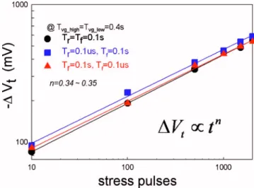
con-sidered to be mainly caused by conventional NBTI degradation.10,13 Figure 4 shows the negative shift of the threshold voltage 共−⌬Vth兲 as a function of stress pulse number under the different
NBTI stress conditions. The Vthwas defined as the gate voltage at which the drain current equals 10 nA in the subthreshold region. It can be seen from Fig.4that these −⌬Vthincrease with an increase in
stress pulse number, showing power law dependence. The exponent factor n can be extracted from the power law relationship, Vth = Atn,14 where n is approximately 0.34 in this experiment. This value indicates that the diffusion-controlled electrochemical reaction
is the principal degradation mechanism for all the NBTI stresses.15 These results are similar to those of our previous study,16 which found that NBTI degradation originated from the interface state共Nit兲
increase and grain boundary trap共Ntrap兲 increase. In order to under-stand the influences of rise and fall times on NBTI stress more clearly, the Nitand the Ntrapincrease for all stress conditions will be
analyzed.
The Nitcan be extracted from the S.S by ignoring the depletion
capacitance in the active layer according to the following equation,17 with Nittrap increase occurring not only at the SiO2/poly-Si inter-face but also in the grain boundary in the weak inversion region. Here, the subthreshold swing is defined as half the gate voltage necessary to increase the drain current by 2 orders of magnitude 共from 10−11to 10−9A兲 in the subthreshold region
Nit=
冋
冉
S ln 10冊冉
q kT冊
− 1册
冉
Cox q冊
关1兴Figure5ashows the correlation between the Nitincrease and the number of stress pulses for the three different rise and fall times. It is apparent that the Nitincrease is independent of rise and fall times.
The nearly identical Nitincrease for these different stresses is due to
the same Tvg_highand Tvg_low. The degradation was mainly due to the H dissociation caused by inversion holes during Tvg_high and the
dissociated H recovery during Tvg_low.
The Ntrapincrease can be estimated by the Levinson and Proano
method,4,18such that it includes the Nit. The relationship between
the Ntrapincrease and the number of stress pulses is shown in Fig.
5b, where it is clear that the Ntrap increase is more serious under
stress with a shorter rise time but was independent of fall time. In n-channel TFTs, the main degradation mechanism was by the drain-avalanched hot-carrier induced impact ionization as a result of car-riers being emitted from trap states when fall time is less than 1 ms.19However, in our experiment, the turn-off voltage was only 0 V and the ionization rate of the hole was lower than the ionization rate of the electron.20Therefore, the degradation of the grain bound-ary near the source/drain caused by the emitted carriers did not occur in this experiment. In order to understand the dominant mechanism in the Ntrapincrease for the short rise time, both the input gate voltage and the corresponding bulk voltage共Vbulk兲 were
moni-tored by a digital oscilloscope, as shown in Fig.6. The source was grounded, and the drain was connected to the 2-channel of the digi-tal oscilloscope while the temperature was 125°C. The pulse voltage was applied to gate from the pulse generator and was connected to the 1-channel.
Figure 2.共Color online兲 Waveform of stress pulse applied to the gate.
Figure 3.共Color online兲 Id–Vgtransfer characteristics when the device
op-erates in the linear region for the LTPS TFT at the initial condition and standard NBTI stress condition.
Figure 4. 共Color online兲 Relationship between negative threshold voltage shift and number of stress pulses.
The relationship between the bulk voltage共Vbulk兲 and the gate voltage共Vg兲 is shown in Fig.7aandbfor Trof 0.1s and 1 ms, respectively. It can be seen from Fig.7athat there was a transient increase in the voltage of poly-Si bulk when the gate voltage was switched from 0 to − 20 V in a very short rise time共Tr= 0.1s兲. As the rise time is short, the inversion layer is not immediately formed at the interface between the SiO2and poly-Si, and the ap-plied gate voltage is partially dropped at the bulk region, causing the transient bulk voltage increase. The typical turn-on time of the c-Si FETs is a few tens of nanoseconds.21This experimental result sug-gests that the switching delay in LTPS TFTs can be attributed to the high trap density. Figure7b shows the gate voltage switched from
0 to − 20 V over a long rise time共Tr= 10 ms兲. Clearly, the Vbulk remains at 0 V, even during the transient time, because the inversion charges move along the channel as the gate pulse varies, finally electrically connecting the source and the drain. Therefore, the Vbulk
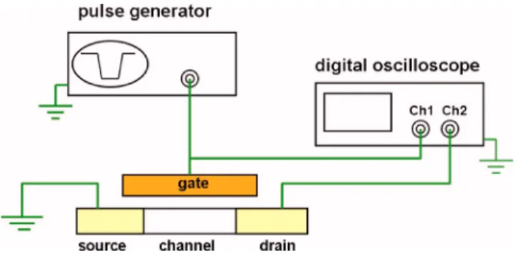
is the same as the source voltage. Based on these results, we further analyzed the transient effect on drain current using a transient mea-surement system, as shown in Fig.8. The gate terminal was con-nected to the 1-channel of the pulse generator and the digital oscil-loscope, and the gate bias was changed from 0 to − 20 V. The drain was connected to the 2-channel of the pulse generator, which was switched from 0 to − 0.1 V. The source was connected to the input of a current-to-voltage converter共Keithley 428兲 such that the output voltage signal and the corresponding drain current could be
Figure 5.共Color online兲 Relationship between 共a兲 Nitincrease and共b兲 Ntrap increase under different number of stress pulses.
Figure 6.共Color online兲 Schematic view of an installation used to monitor Vbulk. The source was grounded, and the drain was connected to the 2-channel of the digital oscilloscope.
Figure 7.共Color online兲 Relationship between bulk voltage and gate voltage for rise times of共a兲 0.1 s and 共b兲 10 ms.
displayed by the 2-channel of the digital oscilloscope. The measure-ment temperature was set to 125°C. The result of the transient cur-rent measurement was shown in Fig.9.
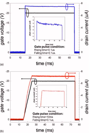
Figures9aandbshow the relationship between the gate voltage and the transient drain currents under rise times of 0.1s and 0.1 ms, and the insets show only the transient drain current during the turn-on region. It can be seen from Fig.9a, that the measured drain current exhibits the peak current at the beginning of the turn-on region and slowly returns to a steady current with the in-creasing measurement time. This phenomenon can be explained by recalling that, in Fig. 7a, the inversion layer is not immediately formed at the SiO2/poly-Si interface, causing the transient bulk
volt-age in poly-Si bulk. When the negative voltvolt-age drops in the poly-Si bulk, holes will diffuse from the p-type source/drain into the Si bulk due to the forward bias. Therefore, excess holes cause the peak transient current to occur at the beginning of the turn-on region.22 The corresponding energy band diagram is shown in Fig.10. On the contrary, for a long rise time of 10 ms, the transient current is fixed to the steady value共steady-state current兲 during the turn-on time because the holes共inversion charges兲 can respond to the variation in the gate voltage.
Figure 10 shows the schematic energy band diagram of LTPS TFTs during different rise times. In the short rise time because the inversion layer is not formed immediately during such a short rise time, surface band bending is not apparent and part of Vgbecomes dropped into the poly-Si bulk, resulting in excess holes diffusing from the source/drain. This phenomenon is also consistent with the result shown in Fig.7aand9a. Because there are many passivated
Si–H bonds in grain boundaries in the poly-Si bulk region, the re-action between the transient-effect-induced excess holes and the Si–H bonds will cause a more serious Ntrapincrease in the poly-Si
bulk during the NBTI stress. In addition, in the long rise time con-dition, the inversion layer forms immediately. Consequently, the main influence of the Ntrapincrease was the steady-state current.
Conclusion
In this work, dynamic NBTI stress in p-channel LTPS TFTs un-der different rise and fall times is investigated. Degradation occurred to the threshold voltage, subthreshold swing, and on-current in all kinds of dynamic NBTI stresses. For shorter and longer pulse rise time, the Nitincrease is similar due to the dissociation of inversion holes and H at the interface at Tvg_high. Nevertheless, for a very short
rise time, a pronounced Ntrapincrease is observed. This is because the inversion layer is not formed immediately and part of the gate voltage Vgis dropped into the poly-Si bulk, inducing excess holes.
Therefore, the transient-effect-induced excess holes are the main reason for the more serious Ntrapincrease in the poly-Si bulk.
Acknowledgments
The work was supported by the National Science Council under contract NSC-99-2120-M-110-001 and 97-2112-M-110-009-MY3.
National Sun Yat-Sen University assisted in meeting the publication costs of this article.
References
1. H. Kuriyama, S. Kiyama, S. Noguchi, T. Kuahara, S. Ishida, T. Nohda, K. Sano, H. Iwata, S. Tsuda, and S. Nakano, Tech. Dig. - Int. Electron Devices Meet., 1991, 563.
2. W. B. Tam and T. Shimoda, SID Int. Symp. Digest Tech. Papers, 2004, 1406. 3. Y. Matsueda, R. Kakkad, Y. S. Park, H. H. Yoon, W. P. Lee, J. B. Koo, and H. K.
Chung, SID Int. Symp. Digest Tech. Papers, 2004, 1116.
4. K. Yoneda, R. Yokoyama, and T. Yamada, in Symposium on VLSI Circuits
Pro-ceedings, IEEE, p. 85共2001兲.
5. H. Tokioka, M. Agari, M. Inoue, T. Yamamoto, H. Murai, and H. Nagata, Proc.
Soc. Inf. Display, IEEE, 280共2001兲.
6. Y. Toyota, M. Hatano, T. Shiba, and M. Ohkura, IEEE Trans. Electron Devices, 54, 2452共2007兲.
7. T. M. Pan, and C. H. Liu, Electrochem. Solid-State Lett., 8, G348共2005兲. 8. G. Chen, M. F. Li, C. H. Ang, J. Z. Zheng, and D. L. Kwong, IEEE Electron
Device Lett., 23, 734共2002兲.
9. J. C. Liao, Y. K. Fang, C. H. Kao, and C. Y. Cheng, IEEE Electron Device Lett.,
29, 477共2008兲.
10. C.-Y. Chen, J.-W. Lee, S.-D. Wang, M.-S. Shieh, P.-H. Lee, W.-C. Chen, H.-Y. Lin, K.-L. Yeh, and T.-F. Lei, IEEE Trans. Electron Devices, 53, 2993共2006兲. 11. V. Huard, C. Parthasarathy, N. Rallet, C. Guerin, M. Mammase, D. Barge, and C.
Ouvrard, in Proceedings of the IEDM, 797共2007兲.
12. V. Huard, M. Denais, F. Perrier, N. Revil, C. Parthasarathy, A. Bravaixc, and E. Figure 9. 共Color online兲 Relationship between the transient drain current
and the gate voltage for rise time of共a兲 0.1 s and 共b兲 10 ms, insets show the transient drain current under turn-on region.
Figure 10.共Color online兲 Energy band diagram of LTPS TFT under different rise times.