IEEE ELECTRON DEVICE LETTERS, VOL. 26, NO. 9, SEPTEMBER 2005 643
A Simple and Low-Cost Method to Fabricate TFTs
With Poly-Si Nanowire Channel
H.-C. Lin, Senior Member, IEEE, M.-H. Lee, C.-J. Su, T.-Y. Huang, Fellow, IEEE, C. C. Lee, and Y.-S. Yang
Abstract—A very simple and low-cost scheme is proposed for fabricating thin-film transistors with poly-Si nanowire (NW) chan-nels. In this scheme, the poly-Si NW channel is formed by clev-erly employing the poly-Si sidewall spacer technique. In addition, the poly-Si NW channel is genuinely exposed to the environment after the poly-Si sidewall spacer formation in the new scheme. This unique feature, together with its simplicity and low-cost, makes this approach very suitable for applications and manufacturing of bio-logic sensing devices. Good device performance is demon-strated in this letter.
Index Terms—Nanowires, poly-Si, sensor device, thin-film tran-sistors (TFTs).
I. INTRODUCTION
F
IELD-EFFECT TRANSISTORS (FETs) built on Si nanowire (NW) channels have recently received lots of attention. Since the surface-to-volume ratio of a semiconductor wire is inversely proportional to its diameter or feature size, characteristics of an NW device would be significantly affected by the surface condition during operation. This property makes the NW attractive for a number of applications, including nano-scale CMOS [1], memories [2], large-area electronics [3], [4], light-emitting devices [3], and sensors for sensing chemical or biological species [5], [6]. Among these applications, the NWs are traditionally prepared by either top-down [1], [6] or bottom-up approaches [2]–[5]. The top-down approaches typically employ advanced optical or e-beam lithography tools to generate the NW patterns. Although compatible with mass-production, the use of advanced lithography tools with nanometer size resolution is costly. On the other hand, the bottom-up approaches usually employ metal-catalytic growth for preparation of NWs. The later approaches, however, suffer seriously from the difficulty in precisely positioning the device location. Metal contamination and control of structural parame-ters are additional issues that need to be addressed for practical manufacturing.Previously, the sidewall spacer formation technique has been proposed to define the nano-scale hardmask itself, with subse-quent etching step to pattern the target materials underneath the hardmask [7]. In contrast, we propose instead to define directly
Manuscript received May 18, 2005. This work was supported in part by the National Science Council of the Republic of China under Contract NSC 93-2215-E-009-79. The review of this letter was arranged by Editor J. Sin.
H.-C. Lin, M.-H. Lee, C.-J. Su and T.-Y. Huang are with the Department of Electronics Engineering, National Chiao Tung University, Hsinchu 300, Taiwan, R.O.C.
C.-C. Lee and Y.-S. Yang are with the Department of Biological Science and Technology, National Chiao Tung University, Hsinchu 300, Taiwan, R.O.C.
Digital Object Identifier 10.1109/LED.2005.853669
Fig. 1. (a)–(d) Key fabrication flow, (f) top view of the device structure, and (e) cross-sectional view along the dashed line A to B in (f).
the nano-scale Si lines that serve as the device channel in this letter. This method is therefore very simple. It is also repro-ducible and suitable for low-cost manufacturing.
II. DEVICEFABRICATION
The key device fabrication steps are illustrated in Fig. 1. Briefly, a gate (n poly-Si) was first formed on a Si substrate capped with an oxide layer [Fig. 1(a)], followed by the de-position of a chemical vapor dede-position (CVD) oxide layer serving as the gate dielectric [Fig. 1(b)]. An a-Si layer was then deposited by low-pressure (LPCVD) [Fig. 1(c)]. Next, an annealing step was performed at 600 C in N ambient for 12 h to transform the a-Si into poly-Si. Subsequently, source/drain (S/D) implant was performed (Fig. 1(d)). Note that the implant energy was kept low so that most implanted dopants were located near the top surface of the Si layer. S/D photoresist patterns were then formed on the substrate by a standard lithography step. A reactive plasma etch step was subsequently used to remove the a-Si layer. It should be noted that the sidewall Si channels were formed in this step in a self-aligned manner [Fig. 1(e)]. Note that the implanted dopants in places other than S/D regions were removed during the etch step due to the shallow project range just mentioned. Afterwards, the S/D dopants were activated by an annealing treatment. The fabrication was completed after the formation of test pads using
644 IEEE ELECTRON DEVICE LETTERS, VOL. 26, NO. 9, SEPTEMBER 2005
Fig. 2. Subthreshold characteristics of a fabricated device.
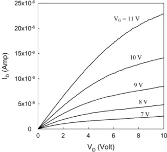
Fig. 3. Output characteristics of a fabricated device.
standard metallization steps. Top view of the fabricated device is shown in Fig. 1(f) (note that for the sidewall Si layer only the regions between the source and drain are shown). Note that the n poly-Si side-gate could be used to adjust the channel potential, thus controlling the devices switching behavior.
III. RESULTS ANDDISCUSSION
Subthreshold and output characteristics of a typical poly-Si NW TFT device are shown in Figs. 2 and 3, respectively. In this example, the height of the n poly-Si electrode is 100 nm, while the thickness of the deposited Si layer and gate oxide are 100 and 30 nm, respectively. After etching, vertical thickness of the channel [see Fig. 1(e)] is reduced to around 30 nm as determined by TEM analysis, as shown in Fig. 4. Channel length is 5 mi-crometers. As can be seen in Figs. 2 and 3, good device perfor-mance with high on/off current ratio (around ) and reason-able subthreshold swing (0.6 V/dec) is achieved, even though
Fig. 4. TEM cross-sectional view of the test device.
the channel material quality and device structure are not opti-mized. The leakage current is rather high, presumably related to the process-induced damage during plasma etching. This issue could be alleviated by optimizing process parameters or using lightly doped drain (LDD) structure. It is also expected that the device performance could be improved if a hydrogenation step is applied.
The above results clearly indicate that, despite its simplicity, our proposed method is genuinely robust and suitable to produce devices with excellent performance. Probably the major con-cern for our device is the channel crystallinity. This issue could be addressed if advanced Si crystallization techniques, such as metal-induced lateral crystallization (MILC) and excimer laser annealing, are employed. Also should be noted is the unique de-vice structure. As can be seen in Fig. 1(e), a significant portion of the poly-Si NW channel is genuinely exposed to the environ-ment in our device structure. This lends itself nicely to chemical and biologic sensor applications, since the exposed channel re-gion could serve as the sensing site [5], [6]. For practical appli-cations, an appropriate bias could be applied to the sidegate so that the channel potential could be tuned to a level that is most sensitive to the concentration variation of the target species. This also implies that the complicated channel doping step used in conventional NW device fabrications [8] could be skipped in our approach.
IV. CONCLUSION
In summary, we have proposed a very simple method for fabrication of thin-film transistors with poly-Si NW channels. Throughout the fabrication, no expensive lithography tools are needed for definition of nano-scale patterns. The fabricated de-vices exhibit good performance, indicating that the proposed method, albeit low-cost and simple, is potentially suitable for future practical manufacturing.
ACKNOWLEDGMENT
The authors would like to thank the National Nano Device Laboratories (NDL) for assistance in device fabrication.
LIN et al.: SIMPLE AND LOW-COST METHOD TO FABRICATE TFTs 645
REFERENCES
[1] F. L. Yang et al., “5 nm-gate nanowire FinFET,” in Symp. VLSI Tech.
Dig., 2004, pp. 196–197.
[2] X. Duan, Y. Huang, and C. M. Lieber, “Nonvolatile memory and pro-grammable logic from molecule-gated nanowires,” Nano Lett., vol. 2, no. 5, pp. 487–490, 2002.
[3] M. C. McAlpine, R. S. Friedman, S. Jin, K. Lin, W. U. Wang, and C. M. Lieber, “High-performance nanowire electronics and photonics on glass and plastic substrates,” Nano Lett., vol. 3, pp. 1531–1535, 2003. [4] X. Duan, C. Niu, V. Sahi, J. Chen, J. Wallace Parce, S. Empedocles, and
J. L. Goldma, “High-performance thin-film transistors using semicon-ductor nanowires and nanoribbons,” Nature, vol. 425, pp. 274–278, 2003.
[5] Y. Cui, Q. Wei, H. Park, and C. M. Lieber, “Nanowire nanosensors for highly sensitive and selective detection of biological and chemical species,” Science, vol. 293, pp. 1289–1292, 2001.
[6] Z. Li, Y. Chen, X. Li, T. I. Kamins, K. Nauka, and R. S. Williams, “Se-quence-specific label-free DNA sensors based on silicon nanowires,”
Nano Lett., vol. 4, pp. 245–247, 2004.
[7] Y.-K. Choi, J. Zhu, J. Grunes, J. Bokor, and G. A. Somorjai, “Fabrication of sub-10-nm silicon nanowire array by size reduction lithography,” J.
Phys. Chem. B, At. Mol. Opt. Phys., vol. 107, p. 3340, 2003.
[8] Y. Cui, X. Duan, J. Hu, and C. M. Lieber, “Doping and electrical trans-port in silicon nanowires,” J. Phys. Chem. B, At. Mol. Opt. Phys., vol. 104, pp. 5213–5216, 2000.