國
立
交
通
大
學
資訊科學與工程研究所
碩
士
論
文
在異質雙核心平台上設計與分析
動態分工的視訊解碼器
Design and Analysis of a Dynamic Task Partitioning Approach
for Video Decoding on Heterogeneous Dual-core Platforms
研 究 生:沈宗範
指導教授:蔡淳仁 教授
在異質雙核心平台上設計與分析動態分工的視訊解碼器
Design and Analysis of a Dynamic Task Partitioning Approach for Video
Decoding on Heterogeneous Dual-core Platforms
研 究 生:沈宗範 Student:Tsung-Fan Shen
指導教授:蔡淳仁 Advisor:Chun-Jen Tsai
國 立 交 通 大 學
資 訊 科 學 與 工 程 研 究 所
碩 士 論 文
A ThesisSubmitted to Institute of Computer Science and Engineering College of Computer Science
National Chiao Tung University in partial Fulfillment of the Requirements
for the Degree of Master
in
Computer Science
June 2008
Hsinchu, Taiwan, Republic of China
Abstract
This thesis presents the design of a video decoder to demonstrate the advantages of dynamic task partitioning for multimedia applications on heterogeneous embedded dual-core systems. Typical application processors for mobile devices are composed of a RISC core for control tasks and a DSP core for data stream processing. For such systems, a common design practice is to perform static task partitioning at design time. Task assignments to each core is fixed and do not change according to runtime system behavior. In this thesis, we proposed a dynamically partitioned approach where the task partitioning across heterogeneous cores is done at runtime. An MPEG-4 Simple Profile video decoder has been implemented using this approach on a TI OMAP 5912 platform for the analysis. Comparing to a decoder optimized for the DSP core, the performance gain is about 40% on average. We also demonstrated that the gain from dynamic task partitioning is even larger than the static partitioning approach when the cores are running other tasks. The experimental results show that dynamic task partitioning on heterogeneous dual-core systems can achieve more than 40 fps of QVGA video decoding at 96 MHz clock rate even when one of the cores is loaded with other tasks.
Acknowledge
能夠完成本論文,我要感謝我的指導教授蔡淳仁博士。這兩年的研究所求學 過程中,感謝老師對我細心的指導,老師對研究上嚴謹的態度以及實事求是的精 神,讓我學習到很多專業的知識。還要感謝嵌入式多媒體系統實驗室的學長、同 學以及學弟妹,在實驗室大家彼此互相幫助、學習成長。最後我想謝謝我的家人 與朋友,有你們的支持以及鼓勵,讓我可以完成碩士論文。Content
Chapter 1.
Introduction...1
1.1. Motivation...1
1.2. Heterogeneous Dual-Core Processors...1
1.2.1. The OMAP 5912 ...2
1.2.1.1. The ARM Core...3
1.2.1.2. The DSP Core ...3
1.2.1.3. OSK 5912...4
1.2.2. Inter-Processor Communication Mechanisms of OMAP 5912 ...6
1.2.2.1. MPUI Interface (MPUI)...6
1.2.2.2. MPU/DSP Shared Memory...6
1.2.2.3. MPU/DSP Mailbox ...7
1.3. Scope of the Thesis ...7
Chapter 2.
Previous Work ...9
2.1. Static Task Partitioning ...9
2.2. Dynamic Task Partitioning...10
Chapter 3.
Optimization for DSP Architecture ...15
3.1. Overall Architecture of Optimized DSP Decoder...15
3.1.1. Memory Map of the DSP Video Decoder ...15
3.1.2. Bitstream File Format Used in this Thesis...18
3.1.3. Intra Frame Decoding Flow ...19
3.1.4. Inter Frame Decoding Flow ...20
3.2. Detail Optimization Techniques for DSP Architecture ...21
3.2.1. C-code Level Optimization...22
3.2.1.1. Using Function Pointer Array to Replace Switch Statement ...22
3.2.1.2. Using Clipping Table to Replace if Statement...22
3.2.2. Using TI C55x IMGLIB ...22
3.2.2.1. IDCT Routine...23
3.2.2.2. Interpolation Routine ...24
3.2.3. Using Intrinsics ...26
3.2.4. Using MUST_ITERATE Pragma ...27
3.2.5. Using DMA...27
3.2.5.2. Data Transfer for Boundary Pixel Extension ...30
3.2.5.3. Decoding Pipeline Analysis for Top/Bottom Rows of Macroblocks...31
3.2.5.4. Decoding Pipeline Analysis for Middle Rows of Macroblocks..33
3.2.6. Performance Improvement Summary ...35
Chapter 4.
Dynamic Task Partition Framework....37
4.1. Design Issues for Dual-Core Processing...37
4.1.1. Data Accessing Unit Size...37
4.1.2. Endian Issue ...38
4.1.3. Cache Coherency Problem...39
4.2. Inter-Processor Communication of Dual-core Decoding...40
4.3. Global Memory Map of Dynamically Partitioned MPEG-4 Decoder ...40
4.4. Dual-core Decoding Architecture ...41
4.4.1. Task Granularity...42
4.4.2. Mailbox Command API ...43
4.4.3. Task Partitioner and Task Interface...44
4.5. Communication Overhead ...47
Chapter 5.
Experimental Results...49
5.1. Experiment of QCIF Decoding Performance ...49
5.2. Experiment of QVGA Decoding Performance ...52
5.3. Experiment of Adding another Task to DSP Core ...53
Chapter 6.
Conclusions and Future Works ...56
List of Figures
Fig. 1. OMAP 5912 functional block diagram ...2
Fig. 2. The block diagram of C5510 DSP [7] ...4
Fig. 3. The OSK 5912 and Q-VGA display module ...6
Fig. 4. The TCM model in [9] ...11
Fig. 5. The component of Profile and Resource Partitioner [10] ...12
Fig. 6. Structure of a DSP Task execution model [12] ...13
Fig. 7. Memory map of DSP on-chip memory...17
Fig. 8. Memory map of external memory (SDRAM) ...18
Fig. 9. Intra frame decoding flow chart...19
Fig. 10. Intra-macroblock decoding ...20
Fig. 11. Inter frame decoding flow chart...20
Fig. 12. Inter-macroblock decoding ...21
Fig. 13. IMGLIB interpolation...26
Fig. 14. IMGLIB interpolation flow chart...26
Fig. 15. Decoding of top row of macroblocks for QCIF video ...31
Fig. 16. Timing diagram of decoding of top/bottom rows of macroblocks ...32
Fig. 17. Decoding of middle rows of macroblocks for QCIF video ...34
Fig. 18. Timing diagram of decoding of middle rows of macroblocks...35
Fig. 19. Global memory map of the dynamically partitioned MPEG-4 decoder ....41
Fig. 20. Dual-core decoding architecture ...42
Fig. 21. The Task Partitioner and the Task Interface diagram...45
List of Tables
Table 1. Section Descriptions ...16
Table 2. Specification of the IMGLIB IDCT routine ...23
Table 3. Execution time of each IDCT routine ...24
Table 4. Specification of the IMGLIB interpolation routine ...25
Table 5. Improvement of using IMGLIB Interpolation routine...26
Table 6. DMA transfer performance from SARAM to SDRAM...29
Table 7. DMA moves n 3×1 macroblocks from SDRAM to DARAM ...30
Table 8. Definition of M., B. and D...32
Table 9. Execution time of decoding of top/bottom rows of macroblocks...33
Table 10. Execution time of decoding of middle rows of macroblocks ...35
Table 11. Performance improvement of DSP video decoder...36
Table 12. Mailbox command from Task Partitioner to Task Interface ...43
Table 13. Mailbox command from Task Interface to Task Partitioner ...43
Table 14. The local variables inside the Task Partitioner ...45
Table 15. The local variables inside the Task Interface ...46
Table 16. The execution stage of communication via mailbox interrupt...48
Table 17. Processor parameters used for the experiments ...49
Table 18. QCIF decoding performance of 64kbps input bitstream...50
Table 19. QCIF decoding performance of 128kbps input bitstream...51
Table 20. QVGA decoding performance ...52
Table 21. Partition number decoding slice...53
Table 22. QVGA Decoding performance when DSP is busy ...54
Table 23. Task Partition ration of each sequence...55
Chapter 1. Introduction
1.1. Motivation
Many embedded multimedia devices today are built with heterogeneous multi-core platforms. For example, in the dual-core architecture, a general purpose RISC processor core (GPP) and a digital signal processor core (DSP) are integrated into an SoC. Existing task partitioning methodologies for heterogeneous dual-core platforms only adopt static task partitioning policy during design time. Dynamic task partitioning policy is only used for symmetric multi-core platforms [1][2]. Static task partitioning works properly for traditional mobile applications where the GPP core is slow and only suitable for the execution of control tasks. However, new generations of RISC processors are usually powerful enough to take over some of the computationally expensive data stream processing jobs. In addition, multimedia applications for embedded systems have become very sophisticated and their computational resource requirement changes dynamically at run time.
In this thesis, we proposed a dynamic task partitioning paradigm for heterogeneous multi-core platfroms. With this approach, tasks are assigned to different cores dynamically depending on runtime loading of each core. In addition, each core schedules the tasks assigned to them independently to other cores. MPEG-4 simple profile video decoder is used as an example to demonstrate that the dynamic task partitioning approach outperforms the traditional static task partitioning approach significantly. Therefore, it is very promising for practical applications.
1.2. Heterogeneous Dual-Core Processors
applications that are based on heterogeneous dual core architectures. One of the popular processors in this category is the OMAP (Open Multimedia Application Platform) processors designed by Texas Instruments [3][4][5]. In general, the OMAP platforms have dual-core architecture consisting of both an ARM RISC processor core and a TI TMS320 series DSP core.
1.2.1. The OMAP 5912
The OMAP 5912 is a highly integrated hardware and software platform, designed to meet the application processing needs of next-generation embedded devices. The OMAP 5912 couples an ARM926EJ-S RISC core and a TMS320C5510 DSP core. The ARM9 RISC core is very popular for embedded systems and the C5510 DSP core provides high performance with low power consumption. The OMAP 5912 functional block diagram is shown in Fig. 1[6].
1.2.1.1. The ARM Core
The features of the ARM926EJ-S processor core are list as follows: ¾ 192MHz maximum frequency
¾ Support 32-bit and 16-bit (Thumb Mode) Instruction Sets
¾ Support 16K-Byte Instruction cache, 8K-byre data cache, and 17-word write-back buffer
¾ Support Memory management Unit (MMU) and two 64-Entry Translation Look-Aside buffer (TLBs) for MMU
1.2.1.2. The DSP Core
On the DSP side, the features of the TMS320C5510 core are list as follows: ¾ 192MHz maximum frequency
¾ One/Two Instructions Executed per Cycle
¾ Dual Multipliers (Two Multiply-Accumulates per Cycle)
¾ Two Arithmetic/Logic Units and five Internal Data/Operand Buses (3 Read Buses and 2 Write Buses)
¾ 32K×16-Bit On-Chip Dual-Access RAM (DARAM) and 48K×16-Bit On-Chip Single-Access RAM (SARAM)
¾ Support Instruction Cache (16K Bytes)
¾ Support video hardware accelerators for DCT, inverse-DCT, pixel interpolation, and motion estimation for video compression
There are fore man functional units of the DSP, the conceptual block diagram of the DSP is shown in Fig. 2. The C5510 DSP uses instruction pipelining that has two
decoupled segments. The first segment is the fetch pipeline that fetches 32-bit instructions from memory and places them in the instruction buffer queue, and then feeds the second pipeline segment with 48-bit instruction packets. The second segment is the pipeline that decodes instructions and performs data accesses and computations. In addition, the pipeline protection mechanism inserts delay cycles as necessary to prevent read operations and write operations from happening out of the intended order.
Fig. 2. The block diagram of C5510 DSP [7]
1.2.1.3. OSK 5912
In this thesis, the proposed dynamically partitioned MPEG-4 decoder is implemented on the OSK 5912 development board. The OMAP 5912 Starter Kits (OSK 5912) is a development board that integrated an OMAP 5912 chip and also
includes some components as follows: ¾ 32 Mbyte DDR SDRAM
¾ 32 Mbyte Flash ROM
¾ 4 Expansion connectors (bottom side) ¾ RS-232 Serial Port
¾ 10 MBPS Ethernet port ¾ USB Host Port
¾ Compact flash connector
¾ On board IEEE 1149.1 JTAG connector for optional emulation
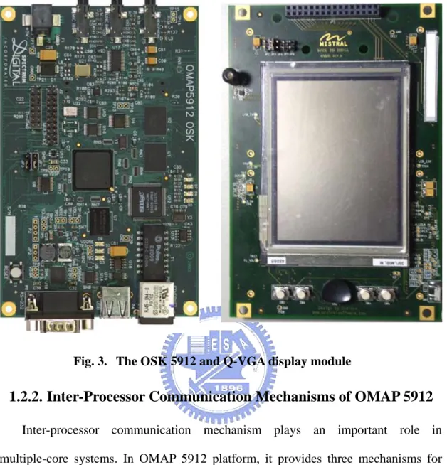
Besides, there is a Q-VGA LCD Module that is also connected to the OSK 5912 development board. We use the Q-VGA module for displaying the decoded frame. The OSK 5912 and the Q-VGA module are shown in Fig. 3.
Fig. 3. The OSK 5912 and Q-VGA display module
1.2.2. Inter-Processor Communication Mechanisms of OMAP 5912
Inter-processor communication mechanism plays an important role in multiple-core systems. In OMAP 5912 platform, it provides three mechanisms for communication between the MPU and the DSP.
1.2.2.1. MPUI Interface (MPUI)
The MPU interface allows the Microprocessor Unit (MPU) and the system DMA controller to communicate with the DSP and its peripherals. The MPUI can access the full memory space (16M bytes) of the DSP. The MPUI is the only way for the MPU to access the I/O space of the DSP.
1.2.2.2. MPU/DSP Shared Memory
shared SRAM and external SDRAM via the traffic controller (TC). The DSP MMU maps the physical address space in shard memory to part of the DSP virtual address space.
1.2.2.3. MPU/DSP Mailbox
The third mechanism for communication between MPU and DSP is through the mailbox. There are four sets of mailbox registers located in public TIPB space. The registers are shared between the two processors, so the MPU and the DSP core may both access these registers within their own public TIPB space, but read/write accessibility of each register is different for each processor. Take ARM2DSP mailbox for example, MPU can read/write the register, but only read the register located in DSP core.
Each set of mailbox registers consists of two 16-bit registers and a 1-bit flag register. When one processor write data to a command register, an interrupt will be issued to the other processor core and sets the corresponding flag register. The interrupted processor core acknowledges this interrupt request by reading the command word, which also clears the flag register.
1.3. Scope of the Thesis
The organization of the rest of the thesis is organized as follows. Chapter 2 introduces some previous work related to task partitioning policy in multiprocessor systems. Chapter 3 describes the architecture and implementation details of a slice-based MPEG-4 video decoder optimized for a DSP processor alone. This optimized DSP-only decoder will be used as the baseline reference to demonstrate the advantage of the proposed dynamic partitioning approach. Chapter 4 presents the proposed dynamic task partitioning approach to MPEG-4 video decoder on dual-core
platforms. The experimental results will be shown in chapter 5 and finally, the conclusion and discussions will be given in chapter 6.
Chapter 2. Previous Work
In multiprocessors systems, task partitioning determines which task should be assigned to which processor, and task scheduling determines when to execute the tasks assigned to a particular processor. Generally speaking, the task partitioning can be roughly divided into two approaches according to the time partition decision is done. The first approach is static partitioning where task partitioning is done at development time. The second approach is dynamic partitioning where task partitioning is done at runtime according to task loading of each core. Although there are some research try to achieve dynamic task partitioning by profiling application at development time and perform dynamic partitioning at run time based on profiling data [9][10] these proposals are for symmetric multi-core systems. The main topic of this thesis is about dynamic task partition on heterogeneous multi-core platforms, which have not been covered by other researchers yet. Therefore, in this chapter, we review some work on static task partitioning on heterogeneous multi-core platforms and dynamic task partitioning for symmetric multi-core platforms.
2.1. Static Task Partitioning
A common practice for task partition on heterogeneous multi-core platforms is to perform static task partitioning. First, profiling and analysis of a system behavior is conducted. Then, task partitioning decision is made based on the computation profile of the system behavior on each cores and the communication profile across different cores.
Take the design in [1] as an example. An MP3 decoding system is implemented in a Motorola DSP 56654 which combines a RISC core and a 16-bit fixed point DSP.
In [1], MP3 decoding algorithm runs on the DSP core and the RISC core is in charge of system management and user interface (UI). The RISC core will receive commands through the UI and assign decoding tasks to the DSP core. However, after the task is assignment, the RISC core will go into an idle state until DSP assert an interrupt to the RISC core to signal the completion of a task. Another example is described in [2]. An MPEG-4 video decoder is implemented on a heterogeneous dual-core platform with a RISC core and a DSP core. In that paper, the DSP core is responsible for video decoding and the RISC core manages the reception of the raw video bitstream from the transmission module and communication with the DSP core.
Static task partitioning is commonly used in industry and may work properly for traditional mobile applications. However, it is not suitable for new generations of complicated embedded multimedia applications.
2.2. Dynamic Task Partitioning
It is quite common that in a mobile multimedia device, several computationally expensive tasks are assigned to the DSP while the RISC (which only handles sporadic UI/system management tasks) is idle. In this case, statically partitioned tasks pre-assigned to DSP at design time may not be able to achieve desirable performance at runtime since the DSP is overloaded. Further more, although the DSP core is heavily loaded in this case, the RISC core is idling most of the time waiting for new tasks to arrive.
New generations of RISC processors are usually powerful enough to take over some of the computationally expensive jobs. Besides, multimedia application has become complicated and dynamic at run time and static partitioning approach may not reach optimal performance when the runtime system state is different from the assumed static state at development time. In dynamic task partitioning, each task is
assigned on the run time according to system state and processing loading of each core.
Lauwereins et al. proposed a TCM (task concurrency management) model and two-phase scheduling method in order to manage concurrent task scheduling into multiprocessor platform [9]. This approach tries to minimize the energy consumption, but also satisfy system timing constraint. The TCM methodology (shown in Fig. 4) comprised of three stages. The first is concurrency extraction. In this first stage, the system extracts and explicitly models the potential parallelism and dynamic behavior of the application. In the second stage, it tries to find the dependency between different tasks. The third stage mainly consists of a two-phase scheduling approach. The two-phase scheduling is static scheduling at design time and dynamic scheduling at runtime. In the first phase, it uses static scheduling to show all possible combination and generate a Pareto-optimal set. In the second phase, select the optimal combination of those tasks. This will minimize the run time computational complexity and lead to power saving.
Xue et al. [10] discuss dynamic partitioning of processor and memory resources in multiprocessor SoC architecture. The proposed approach has two major components, shown in Fig. 5. The first component is the Profiler. The Profiler includes an offline preprocessing of applications which gives us an estimated profile for each application. The second component of the approach is a run-time resource partitioner which partitions both the processing core and memory space among executing application.
Fig. 5. The component of Profile and Resource Partitioner [10]
Chiu et al. [11] proposed a tightly-coupled dual-core partitioning framework for multimedia application on heterogeneous dual-core platforms. In that framework, a task will be dynamically assigned to either the RISC core or the DSP core, depending on the load of each core at runtime. If both cores are available, then tasks will be distributed to both cores for parallel execution. The paper uses MPEG-4 simple profile encoder as an example to investigate proposed tightly-coupled partitioning framework on the TI-OMAP 1510 dual-core platform. The task granularity is set at macroblock level and the experimental results show that dynamic partitioning
approach runs faster than a static task partitioning solution.
Gai et al. [12] investigated the problem of multiprocessor partitioning for heterogeneous architectures composed by a general purpose processor and a DSP. The paper treat DSP core as a functional specific unit and make DSP core execute in a non-preemptive fashion. In order to achieve scheduling efficiently and still maintain some kind of real-time guarantee, the paper improves the Distributed Priority Ceiling Protocol (DPCP). The DPCP was proposed by R. Rajkumar in 1990 [13], where it is used for task allocation on main CPU and DSP. The DPCP is described as follows. A set of n periodic tasks scheduled by the rate-monotonic algorithm can always meet their deadlines if ) 1 2 ( .... 1/ 1 1 2 2 1 1 − ≤ + + + n n T C T C T C T: period time C: computation time
The real-time task model is considered in Fig. 6. Each task execute CiDSP units of
time, and Cipre、Cipost units of time of pre-process and post- process. Besides, define
Ci= Cipre + Cipost, and Pi is the priority of the job i.
As a result, according to the DPCP approach, the schedulability of the task set is guaranteed by the following test:
) ( T C C T C C ,..., 1 lub i DSP i i j DSP j j i U B n i i p pj i ≤ + + + + = ∀
∑
> Where ( ) (21/ 1) lub = − i i iU ,and Bi is a blocking factor computed as follows:
⎪ ⎩ ⎪ ⎨ ⎧ ⎥ ⎥ ⎥ ⎤ ⎢ ⎢ ⎢ ⎡ + = <
∑
> sk regular ta a for 0 task a DSP for C } { max DSPj i j i j P P j i DSP j P P i T T C BHowever, in the above formula, Ci unit of time is the master processor processing
time, and it can be remove from the above formula. Therefore, this paper proposes a modified DPCP approach and removes the master processor processing time (Ci).
Finally, simulations have shown that modified DPCP always outperforms the original DPCP protocol and achieves a significant improvement for large task sets with high processor utilization.
Chapter 3. Optimization for DSP
Architecture
In this chapter, we present a slice-based MPEG-4 video decoder optimized for DSP architecture. For the proposed dynamic task partitioning decoder, a video slice will be used as a task unit. Therefore, optimized implementations of slice decoding modules for the RISC core and the DSP core are necessary to achieve good performance. Optimization of a video slice decoder for a RISC core is quite trivial while optimization for a DSP core is relatively more complex. The performance of the optimized DSP video decoder is comparable to that of the optimized OMAP video decoder published by TI [19]. In the following sections, we will describe the decoder architecture in detail.
3.1. Overall Architecture of Optimized DSP Decoder
Before we present some detail optimization techniques, the overall architecture of the DSP decoder is presented in this section. The key issue of optimizing a video decoder for the DSP core is to take advantage of the multiple memory banks available in the system to increase data bandwidth. Hence, in section 3.1.1, we begin our discussion with the way memory banks in the OMAP platform are used by the optimized video decoder.
3.1.1. Memory Map of the DSP Video Decoder
In addition to the external SDRAM and SRAM memory banks that are common for an embedded system, the TI C5510 DSP core has two on-chip memory blocks, including a 64KB dual-access RAM (DARAM) and a 96KB single-access RAM
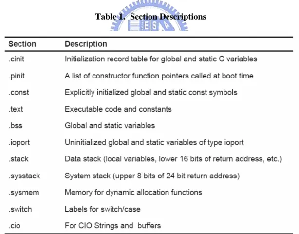
(SARAM). Frequently accessed data should be stored on the on-chip memory due to higher memory bandwidth. However, these on-chip memory blocks are usually too small to contain the entire working set of data of a multimedia algorithm. Take video decoding for example, when decoding an inter frame, the reference frame buffer is frequently accessed for motion compensation. The resolution of the QVGA video frames are 320×240, which means that the frame size is 112.5 Kbytes (with video format YCBCR 4:2:0). The entire reference frame is too big to be placed in the on-chip memory. In this section, we discuss how different memory banks are used for the DSP video decoder. In this thesis, we have used the TI Code Composer Studio (CCS) as the development toolchain. The CCS compiler generates code and data into logical units called sections, as shown in Table 1 [14].
Table 1. Section Descriptions
In Table 1, the .stack and .sysstack sections which store parameters and local variables are accessed frequently within a function calls. Since C55x may issue two
instructions per cycle, simultaneous accesses to more than one parameters and local variables occur frequently. If these sections are allocated in the SARAM block, then additional memory wait cycles will hinder the performance. Hence, we allocate these two stack sections in DARAM. For similar reason, the .bss (which contains global variables) section is also assigned to the DARAM.
Since reference frame will be frequently accessed throughout the decoding of a slice. The performance will suffer significantly if we have to access external memory for the reference frame data. In order to accelerate overall decoding performance, we use the on-chip memory to cache the reference frame data. Two memory buffers, Internal Current Macroblock Buffer (ICMB) and Internal Reference Macroblock Buffer (IRMB), are allocated in the on-chip memory. The IRMB contains some macroblock data of previously decoded frame, and the ICMB is an internal buffer for placing currently decoded macroblock YCBCR data. The on-chip memory map of the
MPEG-4 decoder for the DSP is shown in Fig. 7.
DARAM 64KB SARAM 96KB 0x0000 0x8000 .cinit .switch .cio .const Internal Bitstream Buffer(IBB) ICMB IMGLIB IDCT Buffer IRMB .stack .sysstack .bss .sysmem .vector IMGLIB Interpolation Buffer Clip_table
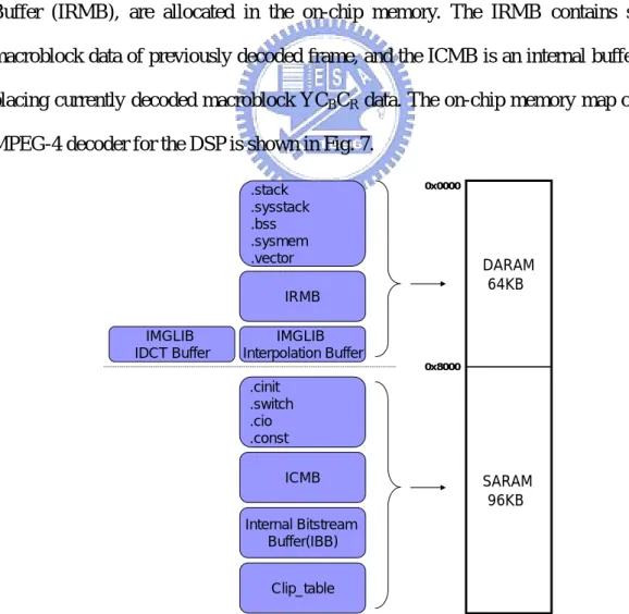
Due to the size limit of the internal memory, some data sections and the code section have to be assigned to the external memory. We can use SDRAM as an external memory space by using the DSP MMU to map part of its virtual memory space to the SDRAM on the MPU side. When the DSP MMU is enabled, the DSP address space starting from 0x050000 to 0xFFFFFF is mapped to the physical SDRAM area that stores shared data between MPU and DSP. Fig. 8 shows the external memory map of the DSP video decoder.
External Input bitstream Output YUV data External Ref. Frame External Cur. Frame
0x10100000 0x10200000 0x10300000 DSP MMU SDRAM 0x10000000 0x200000
.text (Code section)
DSP Virtual Address
Fig. 8. Memory map of external memory (SDRAM)
3.1.2. Bitstream File Format Used in this Thesis
The input bitstream of the mpeg-4 decoder is placed in the external memory (SDRAM). To achieve better decoding performance, we allocated an Internal Bitstream Buffer (IBB) in the on-chip SARAM that is large enough to store bitstream data for one compressed video frame. Before decoding a frame, we need to move the bitstream of the frame into the IBB. Most file formats (such as the ISO MP4 standard) allow quick extraction of one video frame of bitstream data from the raw bitstream. To simplify the file parsing operation, we have designed a very simple file format that stores the bitstream in the following way. The raw video header bitstream data and each video frame of bitstream data are prefixed with a 16-bit length field that specifies
the size (in bytes) of the video header or video frame. These length-prefixed video data units are then stored in a file in decoding order. At decoding time, the decoder can reads the bitstream file sequentially and transfers the bitstream of a single frame into IBB quickly. Since standardized file format (such as the MP4 file) parsing is not the key concern in this thesis, the simplified file format allows us to concentrate on the design of the slice-based decoder.
3.1.3. Intra Frame Decoding Flow
For intra frame decoding, the input bitstream passes through the VLD module, the DC/AC prediction module, the inverse quantization module, and the IDCT module. The intra frame decoding flow chart is shown in Fig. 9.
Bitstream
VLD PredictionDC/AC QuantizationInverse IDCT YCBCR
Bitstream
VLD PredictionDC/AC QuantizationInverse IDCT YCBCR
Fig. 9. Intra frame decoding flow chart
In the proposed framework, the output YCBCR data is places into ICMB. This
buffer can hold 1×6 macroblocks. The size of ICMB is determined according to the DMA throughput analysis experiment to be discusses in section 3.2.5. After decoding an intra frame each time, the decoder will store the output YCBCR macroblock in
ICMB, which acts as a FIFO buffer. When the FIFO buffer is full, all the macroblock data in ICMB will be transferred to the current frame buffer. The current frame buffer is stored in external SDRAM. The intra macroblock decoding diagram is shown in Fig. 10.
Decode
Intra-Macroblock External Cur. Frame
move ICMB
16 16
Fig. 10. Intra-macroblock decoding
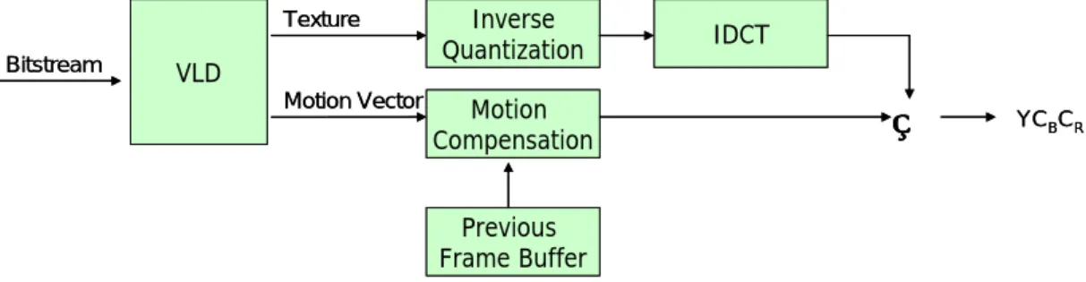
3.1.4. Inter Frame Decoding Flow
For inter frame decoding, the decoding loop is similar to the intra frame decoding loop. The only difference is that the reconstruction of the current macroblock YCBCR
data must accesses the previously decoded frame (called the reference frame) since the motion compensation module need the reference frame to construct the current macroblock predictor. The inter frame decoding flow chart is shown in Fig. 11.
Texture Bitstream VLD
Inverse
Quantization IDCT
Motion Vector Motion
Compensation Previous Frame Buffer
♁
YCBCR Texture Bitstream VLD Inverse Quantization IDCTMotion Vector Motion
Compensation
Previous Frame Buffer
♁
YCBCRFig. 11. Inter frame decoding flow chart
In the proposed architecture, the previous frame buffer in Fig. 11 is the IRMB. The size of the IRMB is only large enough to store 3×8 macroblocks since we must limit the usage of the on-chip memory. However, this size limit assumes that the
f_code in the video bitstream shall be 1 (we will explain the constraint shortly), which conforms to the 3GPP specification for Simple Profile video support. The inter macroblock decoding diagram is shown in Fig. 12.
Decode Inter-Macroblock
External Ref. Frame
move
Reference
External Cur. Frame
move ICMB
IRMB
16 16
Fig. 12. Inter-macroblock decoding
If the f_code is set to 1, when decoding a macroblock, the decoder would only refer to the 3×3 macroblocks in the reference frame around the co-located macroblock of current macroblock. Before the decoding of a new macroblock (except for the boundary ones), 3×1 reference macroblocks will be transferred from the external reference frame buffer into the IRMB. In order to improve the overall decoding performance, we use the DSP DMA for macroblock transfer. The detail analysis about using DSP DMA for macroblock transfer is shown in 3.2.5.
3.2. Detail Optimization Techniques for DSP Architecture
In this section, we discuss the techniques used to optimize the decoding performance on the DSP core. In summary, the techniques used including C-level code optimizations, using IMGLIB functions, using intrinsic functions, and using DSP
DMA to pipeline decoding operations and data transfer operations.
3.2.1. C-code Level Optimization
The original C model of the video decoder was designed for general purpose applications without any architecture dependent optimization. Before the DSP-specific optimizations can be applied, coding styles that are not efficient for embedded processor cores must be modified first. For example, conditional branches, which stall the decoding pipeline should be removed as much as possible.
3.2.1.1. Using Function Pointer Array to Replace Switch Statement
Switch statement contains many comparison operations and conditional jumps. For better efficiency, it can be replaced by function pointer array indexed by the conditional variable of the switch statement. After using function pointer array to replace switch statements in one of the motion compensation function, interpolate8x8_switch(), the function gains 6% improvement by itself.
3.2.1.2. Using Clipping Table to Replace if Statement
Saturation operation is common to signal processing algorithms, including video decoding. There are many modules in MPEG-4 video decoders that clip the out to a range, say 0 ~ 255. If a clipping table is used to implement saturation operation, the computation time improved 64.16% by itself.
3.2.2. Using TI C55x IMGLIB
The C5510 DSP in OMAP 5912 has some hardware acceleration support for image and video processing routines. The routines can be invoked through the TI C55x IMGLIB library API [15]. TI C55x IMGLIB is an optimized image/video processing functions library for C programmers using TMS320C55x DSP. The library
is a collection of 31 high-level optimized DSP functions for the TMS320C55x DSP. It includes many C-callable, assembly-optimized, general-purpose image/video processing routines. The library is implemented using C55x hardware extension instructions, and the source code of the library is available. For video decoding, we used the IMGLIB routines to support IDCT and interpolation functions.
3.2.2.1. IDCT Routine
The TI C55x IMGLIB provides 2-D inverse discrete cosine transform for 8x8 IDCT coefficients. Table 2 shows the specification of the IMGLIB IDCT routine [15].
Table 2. Specification of the IMGLIB IDCT routine IDCT for an 8x8 Image Block Using Built-In Hardware Extensions Syntax void IMG_idct_8x8(short *idct_data, short *inter_buffer);
Inputs:
idct_data: Points to a short format array [0...63]
containing an 8x8 macroblock row by row. Data format is Q13.3.
inter_buffer: Points to a short format array [0...71] used as a temporary buffer that contains intermediate results in the transform.
Outputs:
Arguments
idct_data: Points to a short format array [0...63]
containing an 8x8 macro-block row by row. Data format is Q16.0
Description
The routine IMG_idct_8x8 implements the IDCT using built-in hardware extensions for an 8x8 image block. Input terms are
expected to be signed Q13.3 values, producing signed Q16.0 results. To use this IMGLIB IDCT routine for IDCT, one must use Q13.3 as the input data format. However, most integer IDCT routine uses the input data format Q16.0 [16]. Thus, we need to shift left by 3 bits for each input coefficient. The left-shift operation can be done using intrinsic function _shl(). The IMGLIB IDCT routine is
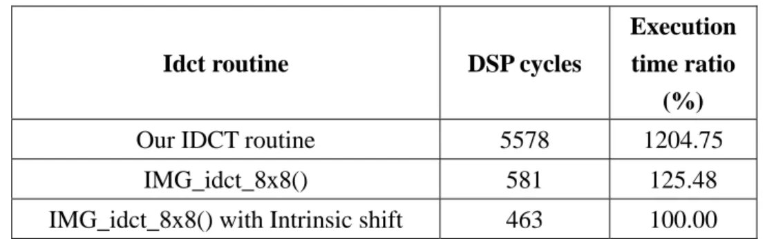
shows the execution time of three IDCT routine.
Table 3. Execution time of each IDCT routine
Idct routine DSP cycles
Execution time ratio
(%)
Our IDCT routine 5578 1204.75
IMG_idct_8x8() 581 125.48
IMG_idct_8x8() with Intrinsic shift 463 100.00 3.2.2.2. Interpolation Routine
The TI C55x IMGLIB provides 16×16 block pixel interpolations which uses built-in hardware extensions. Table 4 shows the specification of the IMGLIB interpolation routine [15]. The IMGLIB interpolation has some difference to the original 8×8 interpolation routine in our C model. First, the input pixel width is 16-bit in the C model, but the IMGLIB interpolation expects the input to be 8-bit per pixel. Second, the IMGLIB interpolation routine processes a 16×16 block, instead of an 8×8 block as the interpolation routine in our C model does. Third, the IMGLIB interpolation routine processes pixel interpolations in the vertical, horizontal, and diagonal directions simultaneously. But for video decoding, we only need interpolation in one of these three directions. Finally, vertical pixel interpolation is a little bit different between the IMGLIB routine and the one in our C model, as shown in Fig. 13.
As a result, we need to do some adjustments to each 8×8 input block. The flow chart is shown in Fig. 14. Simply put, we must pack the input data to fit the IMGLIB interpolation format first, and then shift the position of each pixel to the right by 1 pixel. In addition, we also modified the assembly code of the IMGLIB interpolation routine, because we only need 8×8 block interpolation instead of 16×16.
Table 4. Specification of the IMGLIB interpolation routine Pixel Interpolation for 16x16 Image block using built-in hardware extensions
Syntax IMG_pix_inter_16x16(short *reference_window, short
*pixel_inter_block, int offset, short *align_variable);
Inputs:
reference_window: Points to a packed integer format buffer [0...1152] that contains a 48x48 image block row by row. Must be doubleword aligned. Every four pixels are packed into one 32-bit doubleword. Data format Q16.0.
offset: Specifies the top-left corner index of the 18×18 MBE (MBE=16×16 macroblock + extension) in reference_window. Offset is even because of the doubleword alignment.
align_variable: Configures four alignment cases of the MBE in the reference_window.
Outputs:
Arguments
pixel_inter_block: Points to a packed integer format buffer [0...612] that contains the 36×34 interpolated result. Only the lower 33×33 part that corresponds to the whole 36×34 interpolated zone is usually used. Every four pixels are packed into one 32-bit doubleword.
Description The routine IMG_pix_inter_16x16 implements pixel interpolation for a 16×16 source block located in
reference_window using built-in hardware extensions and it is useful in video compression. To implement full interpolation for the 16×16 source block, the 18x18 MBE (MBE=16×16
macroblock + extension) is needed. The full interpolated zone is composed of 36×34 pixels, but only the lower 33×33 part
corresponding to the full interpolated zone is usually interested. The original pixels and interpolated pixels in the full interpolated zone are organized in different 16 bits to adapt to the related motion estimation technique.
A B C D x Y Z A B C D x Y Z Our interpolation A B C D x Y Z A B C D x Y Z IMGLIB’s interpolation
Fig. 13. IMGLIB interpolation
Source macro block
9
9
Pixels in 16-bit width unit 48
48 9
9 1
Specific input buffer
Pixels in 8-bit width unit Format adjustment Interpolation in IMGLIB Interpolated Macro blocks Rounding Alignment
Fig. 14. IMGLIB interpolation flow chart
Table 5 shows the improvement between two interpolation routines on decoding 300 frames of a 64 kbps QCIF foreman sequence.
Table 5. Improvement of using IMGLIB Interpolation routine
Interpolation routine Timer ticks Execution
time ratio(%)
Original C-model interpolation 17325066 295.31 IMGLIB-based interpolation 5866564 100.00
3.2.3. Using Intrinsics
The C55x CCS compiler provides intrinsic functions, which maps directly to C55x instructions (similar to inline assembly). Those intrinsic functions include lots of basic arithmetic instructions like addition, subtraction, and multiplication. Also included are the saturation operation (but only supports 1- or 2-word size), the rounding operation, shift operation, and the absolute value operation.
In the original C-model of the MEPG-4 decoder, we used some #define to define some simple arithmetic operations, like #define MIN(X,Y) ((X)<(Y)?(X):(Y)).
However, we can use intrinsic functions to replace them. For example, we can use _min(X, Y) to replace the MIN(X, Y).
3.2.4. Using MUST_ITERATE Pragma
The MUST_ITERATE pragma is used to convey programmer’s knowledge about loops to the compiler. It should be used as much as possible to aid the compiler in the optimization of loops. The format of the pragma is:
#pragma MUST_ITERATE(min, max, mult)
All fields are optional, min is the minimal number of iterations of the loop, max is the maximal number of iterations of the loop, and mult tells the compiler that the loop always executes a multiple of mult times. If some of these values are not known until runtime, do not include them in the pragma. The MUST_ITERATE pragma must appear immediately before the loop.
We can use this technique in our c code program, for example, if a loop must iterate 64 times. We can use a MUST_ITERATE pragma to make the compiler generates an efficient hardware loop by the following statement.
#pragma MUST_ITERATE(64,64)
However, according to our experiments, using the MUST_ITERATE pragma in the C model does not gain much improvement at all. The reason is probably because the loop iterations in the C model are usually fixed at compiler time. With level-three optimization and fixed loop iterations, the compiler can achieve the same performance as if the MUST_ITERATE pragma is used.
3.2.5. Using DMA
TI C5510 DSP core includes a DMA(Direct Memory Access) logics for data transfer. DMA can move data without CPU involvement, and allows burst mode
transfer that may not be supported by the processor cores. While the processor core is busy processing data internally, the DMA controller can use the system bus to transfer data simultaneously.
The C5510 DMA [17] has 6 channels where each channel has independent source/destination addresses, priority selection, channel enable control, and interrupt selection. The source/destination memory space for a DMA data transfer can be the external memory interface, SARAM, DARAM, and peripherals (like the serial ports). Besides, DSP DMA support four addressing modes including constant addressing, post-incremented addressing, index addressing, and double-indexed addressing. Those four addressing modes can help us to move data flexibly.
3.2.5.1. DMA Throughput Analysis
Although, DMA can help us to get better performance, we have to determine a reasonable transfer block size for video decoding applications. We conducted two experiments to solve this issue. First, we use the DMA to move n macroblock data from SARAM to SDRAM that simulate the data transfer from ICMB to the external current frame buffer. The experimental result is shown in Table 6. According to the experiment, we can easily see that when n becomes larger, the average moving time per macroblock is decreasing. On the other hand, the ICMB occupies more on-chip memory when n is large. In our design, we set the number of macroblocks to 6 for ICMB to balance between the on-chip memory space used and DMA data transfer performance.
Table 6. DMA transfer performance from SARAM to SDRAM
Unit : DSP cycles # of macroblock Total transfer
time Transfer time per MB 1 979 979.0 2 1483 741.5 3 2023 674.3 4 2511 627.7 5 3037 607.4 6 3583 597.1 7 4086 583.7 8 4580 572.5 9 5133 570.3
Second, we use the DMA to transfer n 3×1 macroblocks from SDRAM to DARAM to simulate the transfer from external reference frame to IRMB. The experimental result is shown in Table 7. According to the experiments, we also know that when n becomes larger, the average moving time per 3×1 macroblock is decreasing. On the other hand, one must take into account the overlap between DMA transfer time and DSP decoding time for pipeline operation. The average time for decoding an inter macroblock is approximately 6612 DSP cycles (see Table 9). As a result, we need to restrict each burst of DMA data transfer time to 6612 cycles in order to arrange for maximal overlap of DSP decoding operation and DMA transfer operation for parallel execution. Finally, in our design, we select n to 1 here that means we move one group of 3×1 macroblocks to internal memory space per inter macroblock decoding.
Table 7. DMA moves n 3×1 macroblocks from SDRAM to DARAM
Unit : DSP cycles
# of 3×1 macroblock groups Total transfer time Transfer time per group
1 2571 2571.0 2 4702 2351.0 3 6809 2269.6 4 8966 2241.5 5 11151 2230.2 6 13232 2205.3 7 15337 2191.0 8 17413 2176.6 9 19535 2170.5
3.2.5.2. Data Transfer for Boundary Pixel Extension
For inter frame decoding, the motion compensation module will reference the previous frame. The motion vector may indicates that compensation from outside the frame boundary is required. Therefore, we need to perform boundary extension from previous frame. In the proposed design, boundary extension is performed on-the-fly when reference data is transferred by the DMA from the external reference frame buffer to the IRMB.
The decoding pipeline is set up so that when the DMA is transferring reference data of macroblock i+1 to on-chip IRMB, the DSP core is decoding macroblock i in parallel. In the next two sections, we perform some analysis on the overlapping operation of the inter frame decoding pipeline. First, in section 3.2.5.3, the case of decoding top/bottom rows of macroblocks are investigated. Then, in section 3.2.5.4, the case of decoding the middle rows of macroblocks is analyzed.
3.2.5.3. Decoding Pipeline Analysis for Top/Bottom Rows of Macroblocks
For top or bottom rows of macroblock decoding, boundary extensions will be performed. The first and the last macroblocks in the top row require boundary extension in three directions. The others macroblocks in the top row only need boundary extension in one direction, as shown in Fig. 15 (the frame size is 176×144 in this example). 16 16 208 176 176 144
Decoding
12 13 14 15 16 17 18 19 20 21 11 1 2 3 4 5 6 7 8 9 10 0 B14 B16 B13 B15 B2 B3 B4 B5 B6 B7 B8 B9 B10 B11 B1 B0 B12 B17 22 23 24 25 26 27 28 29 30 31 32 B18 16 16 208 176 176 144Decoding
12 13 14 15 16 17 18 19 20 21 11 12 13 14 15 16 17 18 19 20 21 11 1 2 3 4 5 6 7 8 9 10 0 1 2 3 4 5 6 7 8 9 10 0 B14 B16 B13 B15 B2 B3 B4 B5 B6 B7 B8 B9 B10 B11 B1 B0 B1 B2 B3 B4 B5 B6 B7 B8 B9 B10 B11B12 B0 B12 B17 22 23 24 25 26 27 28 29 30 31 3222 23 24 25 26 27 28 29 30 31 32 B18Fig. 15. Decoding of top row of macroblocks for QCIF video
When decoding macroblock 0, the decoder must transfer macroblock number 0, 1, 11, 12 from the previous frame buffer to the IRMB first, and then apply boundary extension to create macroblocks B0, B1, B2, B13, and B15 in the IRMB. But when decoding macroblock 1, the decoder just needs to transfer macroblock 2 and 13, and use boundary extension to create macroblock B3 in the IRMB. The timing diagram of the pipeline operation is shown in Fig. 16. The definitions of some symbols in Fig. 16 are explained in Table 8.
Fig. 16 (A) shows sequential operation of the decoding process, while Fig. 16 (B) shows pipeline operation of the decoding process. Obviously, for top/bottom rows of macroblocks, there is not much overlap of execution time between DMA operations and DSP operations. The reason is that we need to make sure the reference data is in the internal buffer first, before we can start the boundary extension process. The measured time of each operation is show in Table 9.
Table 8. Definition of M., B. and D.
Definition Description Example
M. Use DMA to move data
M.(1,2) : Use DMA to move macroblock 1 and macroblock 2
B.
Use DMA to do boundary extension
B.(B0,B1) : Use DMA to do boundary extension for macroblock B0 and macroblock B1
D. Decode an macroblock D.(1) : Decode macroblock 1
… M.(0,1,11,12) B. (B0, B1, B2, B13, and B15 ) M.(2, 13) B.(B3) D. (0) M.(3, 14) B.(B4) D. (1) M.(4, 15) B.(B5) D. (2) M.(5, 16) B.(B6) D. (3) M.(6,17) B.(B7) D. (4) M.(5,6,7,16,17,18) B.(B6,B7,B8) D. (5) 1000 2000 3000 4000 5000 6000
(A) Sequential execution of macroblock decoding and DMA data transfer
M.(5,6 7,16,17,18) M (0,1,11,12) B. (B0, B13 , and B15 ) M. (2, 13) D. (0) M. (3, 14) D. (1) M. (4, 15) D. (2) M. (5,16) D. (3) M. (6,17) D. (4) D. (5) M. (8, 19) B. (B3) B. (B4) B. (B5) B. (B6) B. (B7) B. (B6,B7,B8) … B. (B1,B2) 1000 2000 3000 4000 5000 6000
(B) Overlapped execution of macroblock decoding and DMA data transfer Fig. 16. Timing diagram of decoding of top/bottom rows of macroblocks
Table 9. Execution time of decoding of top/bottom rows of macroblocks Sequential execution (timer ticks) Overlapped execution (timer ticks) DMA Overlapped % D.(x), x=0, 1, 2, … (Decode a macroblock) 412.27 427.51 DSP side: 770.72 M.(0,1,11,12) and
B.(B0,B1,B2,B13,and B15) 840.36 DMA side: 72.34 8 %
†
DSP side: 611.54 M.(5,6,7,16,17,and 18 ) and
B.(B6,B7,and B8) 755.78 DMA side: 149.56 19%
†
DSP side: 284.66 M.(x, x+11) and B.(Bx+1)
(x=2, 3, 4, 5, …) 343.29 DMA side: 60.14 17%
†
†:The overlapped execution percentage is approximation
3.2.5.4. Decoding Pipeline Analysis for Middle Rows of Macroblocks
For each middle row of macroblocks, only the left most and right most macroblocks have to perform boundary extension before decoding. Take the non-top row of macroblocks of frame for example, and the diagram is shown in Fig. 17. We only perform boundary extension for macroblock number B13, B14, B15, B16, B17, and B18 in the previous frame. The timing diagram is shown in Fig. 18. As one can see, the decoding pipeline has much higher degree of overlapping operations in this case.
16 16 208 176 176 144 12 13 14 15 16 17 18 19 20 21 11 1 2 3 4 5 6 7 8 9 10 0 B14 B16 B13 B15 B2 B3 B4 B5 B6 B7 B8 B9 B10 B11 B1 B0 B12 B17 22 23 24 25 26 27 28 29 30 31 32 B18
Decoding
16 16 208 176 176 144 12 13 14 15 16 17 18 19 20 21 11 1 2 3 4 5 6 7 8 9 10 0 B14 B16 B13 B15 B2 B3 B4 B5 B6 B7 B8 B9 B10 B11 B1 B0 B12 B17 22 23 24 25 26 27 28 29 30 31 32 B18 16 16 208 176 176 144 12 13 14 15 16 17 18 19 20 21 11 12 13 14 15 16 17 18 19 20 21 11 1 2 3 4 5 6 7 8 9 10 0 1 2 3 4 5 6 7 8 9 10 0 B14 B16 B13 B15 B2 B3 B4 B5 B6 B7 B8 B9 B10 B11 B1 B0 B1 B2 B3 B4 B5 B6 B7 B8 B9 B10 B11B12 B0 B12 B17 22 23 24 25 26 27 28 29 30 31 3222 23 24 25 26 27 28 29 30 31 32 B18Decoding
Fig. 17. Decoding of middle rows of macroblocks for QCIF video
Generally speaking, we can set three DMA channels to transfer the macroblock reference data of Y, CB, and CR components independently. However, according to our
experiments, using three DMA channels to access the external memory via EMIF (external memory interface) at the same time causes serious degradation of performance. Therefore, we only use one DMA channel to transfer CB, CR, and Y
components sequentially. The measured time of each operation is show in Table 10. With this pipelined design, we have achieved 35% performance improvement compared to the original sequential, un-pipelined decoder C model.
M.(0,1,11, ,12,22,23) B.(B13,B15,B17) M. (2,13 ,24) D.(11) … M. (3,14 ,25) D.(12) M. (4,15 ,26) D.(13) M. (5,16 ,27) D.(14) M. (6,17 ,28) D.(15) M.(5,6,7,16,17,18, 27,28,29) D.(16) 1000 2000 3000 4000 5000 6000
(A) Sequential execution of macroblock decoding and DMA data transfer
M.(0,1,11 ,12,22,23) M. (2,13 ,24) … D.(11) M. (3,14, 25) D.(12) M. (4,15, 26) D.(13) M. (5,16 ,27) D.(14) M. (6,17, 28) D.(15) D.(16) M. (8,19, 30) B. (B13, B15, B17) M. (2,13 ,24) M. (3,14, 25) M. (4,15, 26) M. (5,16 ,27) M. (6,17, 28) M.(5,6,7, 16,17,18 27,28,29) Waiting For DMA 1000 2000 3000 4000 5000 6000 M.(5,6,7, 16,17,18, 27,28,29)
(B) Overlapped execution of macroblock decoding and DMA data transfer Fig. 18. Timing diagram of decoding of middle rows of macroblocks
Table 10. Execution time of decoding of middle rows of macroblocks
Sequential execution (timer ticks) Overlapped execution (timer ticks) DMA Overlapped % D.(x), x=11,12, 13, … (Decode a macroblock) 412.27 427.51 DSP side: 621.66 M.(0,1,11,12,22.23) and
B.(B13,B15,and B17) 799.37 DMA side: 188.32 23%
†
DSP side: 210.31 M.(5,6,7,16,17,18,27,28,
and 29 ) 829.26 DMA side: 661.65 24%
†
DSP side: 190.59 M(x, x’)
(x=13, 14, 15, …) 327.57 DMA side: 141.93 42%
†
†:The overlapped execution percentage is approximation
3.2.6. Performance Improvement Summary
The performance improvements of each of the techniques we have used to optimize the DSP decoder is summarized in Table 11. The target sequence is the 300-frame QCIF version of FOREMAN sequence at 64 kbps. The optimized DSP decoder will be used as the baseline reference to compare against the proposed
approach in Chapter 4.
Table 11. Performance improvement of DSP video decoder
State Item CPU cycles Second FPS
Performance improve
from previous
state
1 Initial MEPG-4 decoder C
model on DSP 2762695282 28.78 10.42 2 Compiler using –o3 and –pm
option 2075085682 21.62 13.88 33.14 %
3 Code section (.text) into
SDRAM 5652045923 58.88 5.10 -63.29 %
4 Enable instruction cache 2173584906 22.64 13.25 260.03%
5
Using intrinsic function in Quantization module for saturation
1677344205 17.47 17.17 29.58 %
6 Using IMGLIB for IDCT
module 1415540100 14.75 20.35 18.49 %
7 Using IMGLIB for interpolation
module 1052574420 10.96 27.36 34.48 %
8 Using ICMB to cache output
data 948365118 9.88 30.36 10.99 %
9
Using IRMB to cache reference data and using DMA for
boundary extension
582313481 6.07 49.45 62.86 %
10 Using DMA for data transfer
and boundary extension 492146185 5.13 58.51 18.32 % 11 Adopt pipeline design 363756454 3.79 79.17 35.30 % 12 Using clipping table for
Chapter 4. Dynamic Task Partition
Framework
Generally speaking, if we want to port a single-core application into the dual-core platforms, we need to partition original application into several sub-tasks. The partitioning methodologies for heterogeneous dual-core platforms typically use static partitioning at development time, and assign each sub-task to either the RISC core or the DSP core, but not both. We proposed a dynamically partitioning approach, and implemented an MPEG-4 decoder on the OSK 5912 platform to demonstrate the efficiency of the proposed approached. The details of the dynamically partitioned MPEG-4 decoder are present in this chapter.
4.1. Design Issues for Dual-Core Processing
Current heterogeneous dual-core systems have some architectural issues that hinder the performance of the dynamic task portioning computation model. These issues are discussed in the next few subsections.
4.1.1. Data Accessing Unit Size
Generally, most common processor use byte as data accessing unit. But some application specific processor may have optimal data accessing unit size. For example, on OMAP 5912, the RISC core is a 32-bit ARM that allows byte addressing while the DSP core is a 16-bit processor that allows only 16-bit word addressing.
Therefore it is not possible to design a single data structure that is optimized for both cores. Since the computation results of one task may become the input of a task
simple (non-optimal) solution to this problem is to set the data access unit size to the least common multiple of the optimal word sizes of the cores. However, for optimal performance, we should either use two heterogeneous cores with same optimal data accessing unit size or design some programmable on-the-fly data conversion (or packing/unpacking) circuitry for shared data structures.
4.1.2. Endian Issue
In the mix-endian systems, endian conversion may be required if a processor accesses a memory region containing data stored in a different endianness format. For example, if a big-endian processor accessing data stored in little-endian format, then the endianness conversion may be required. Special circuitry should be available to take care of the endian issue in mix-endian heterogeneous multi-core systems.
Within the OMAP5912 device, the ARM operates in little-endian mode, DSP uses the big-endian data format. However, in the OMAP5912 device, it has endianness conversion circuitry. When DSP or DSP DMA accesses to external memory regions, there is an endianness conversion unit inside the DSP MMU. On the other hand, when the MPUI accesses to the DSP resources, there is an endianness conversion within the MPU interface.
In the bitstream parsing of MPEG-4 decoder, it has a byte and word swap computation. However, DSP core will get input bitstream from the SDRAM via DSP MMU. As a result, we do not need to perform byte and word swap if we enable the endianness conversion unit inside the DSP MMU.
According to our experiment, the endianness conversion circuitry only can be set on the booting time. In the DSP core of dual-core decoding, if we enable the endianness conversion, it will affect not only the input bitstream but also the output
decoded frame. According to our experiment, disable the endian conversion circuitry will gain better performance than enable it. This is we do the software endianness conversion on input bitstream is less computation than on the output decoded frame.
4.1.3. Cache Coherency Problem
Most high performance processors core today have data cache. In a dynamic task partitioning system, this may cause serious issue since the shared data processed by a sequence of tasks may be cached differently on different processor cores. Consider a situation as following. When a processing core accesses to a memory location and saves the data inside its cache. Later, the other processing core is processing and writing data to this same location. However, since this memory location is kept in the cache of first core, the first processing core may read the old data instead of new data. The problem is cache coherency problem.
A trivial solution is to disable caching of the shared data. However, this affects the performance of many processor cores. Therefore, scratch pad memory should be used wisely to alleviate the performance hit due to disabling of data cache. For example, on OMAP 5912, there are two in-core memories (SARAM and DARAM) that should be used properly.
On the dual-core processing MPEG-4 decoder, the ARM core and the DSP core share the current decoded frame and reference frame on SDRAM. We can disable those memory regions, but the performance of the decoding will decrease obviously. In the proposed design, we still enable the data cache of the ARM core, because the cache coherency problem does not happen exactly. The DSP core write decoded slice to the share memory region and ARM core refer to those data in next decode slice. However, the size of the data cache of ARM core is 8k byte. When the ARM core
cache of the memory region that contains reference frame and current frame because of the performance consideration.
4.2. Inter-Processor Communication of Dual-core Decoding
As we mentioned in section 1.2.2, there are three mechanisms for communication between the ARM core and the DSP core. In our proposed dynamically partitioned dual-core decoding, we use those mechanisms for communication between the ARM core and the DSP core.
First of all, large amount of shared video data is placed in SDRAM so that both cores can access these data directly. A module, refer to as the Task Partitioner, in the proposed architecture is in charge of dynamic assignment of task to either ARM core or the DSP core. The Task Partitioner is running on the ARM side and therefore it requires inter-processor communication mechanism to communicate with the DSP as well. Mailbox mechanism is used by the Task Partitioner to communicate with the DSP core.
4.3. Global Memory Map of Dynamically Partitioned
MPEG-4 Decoder
The global memory map of the dynamically partitioned MPEG-4 decoder is shown in Fig. 19. For the DSP core, the memory map is the same as the optimized DSP decoder described in Chapter 3. For the ARM core, all the data are located in the SDRAM. The ARM cache is turned on to improve data access performance.
DARAM (64K bytes) SARAM (96K bytes) Memory map on DSP 0×00 0000 0×01 0000 SDRAM (32M bytes)
Memory map on ARM
0×1000 0000 MPUI DSP MMU 0×08 0000 Code section Data section Input bitstream Reference frame QVGA Frame buffer Current frame IRMB IMGLIB Buffer Data section Internal Bitstream Buffer (IBB) ICMB Clipping table Macroblock Info. : DSP access only : ARM access only : Both ARM / DSP access
Code section
0×E000 0000
Fig. 19. Global memory map of the dynamically partitioned MPEG-4 decoder
There are five boot modes for the DSP bootloader. The MPU core can select any of these boot modes by writing to the DSP_BOOT_CONFIG register. The address 0x80000 is the boot address of the external memory boot mode [18]. The code section of DSP is stored in SDRAM and is mapped to 0x80000 in the DSP virtual memory space by the DSP MMU. The DSP instruction cache is also enabled to accelerate instruction fetch performance.
4.4. Dual-core Decoding Architecture
In the proposed dynamic task partitioning framework, the task is dynamically partitioned according to runtime loading of each core. A system control module called the Task Partitioner, which is responsible for dynamic task assignment, is running on the ARM core, and communicates with the DSP core via mailboxes. On the other hand, there is a Task Interface running on the DSP core which is waiting to receive the tasks assigned by the Task Partitioner. The dual-core decoding architecture is shown in Fig. 20.
Initialization
(I-cache enable, Global interrupt)
Task Partitioner DSP core Assign task Response Task Interface Processing Task Finish Waiting Finish Decoding ARM core Initialization
(DSP MMU, Global interrupt, Timer)
Get input bitstream
Fig. 20. Dual-core decoding architecture
4.4.1. Task Granularity
The experimental results in [11] show that dynamic partitioning could increase the overall performance. However, the experiments also show that the inter-processor communication overhead is a crucial factor for such systems. Therefore, the choice of task granularity is crucial for the performance of a dynamic task partitioning system. If the task granularity is too small, the communication overhead between two cores may out-weight the performance gain from parallel execution of the tasks. On the other hand, if the task granularity is too large, then the computation model would falls back to the static task partition model.
The task granularity is defined at the slice-level for the proposed MPEG-4 video decoder. In a video bitstream, each slice includes a start code followed by a sequence of coded macroblocks, and there is no dependency between two different slices. Thus, a video decoder application can quickly locate the bitstream data required by a task (i.e. decoding of a slice) and dynamically assign the task either to the ARM core or the DSP core. Parallel execution is achieved automatically if both cores are available.
4.4.2. Mailbox Command API
The ARM core (Task Partitioner) and DSP core (Task Interface) communicate with each other via mailbox interrupt mechanism. In our proposed design, there are four mailbox command APIs from Task Partitioner to Task Interface, and shown in Table 12. Each mailbox command API including command register field and data register field. On the other hand, there are five mailbox command APIs from Task Interface to Task Partitioner, and shown in Table 13. The Task Partitioner and Task Interface share those commands, and when a core invoke a mailbox command interrupt, the interrupt service routine of the other core will do the corresponding work according to the mailbox command register field.
Table 12. Mailbox command from Task Partitioner to Task Interface
Command register field Data register field Description
A2D_INITIALIZE_DEOCDER Bitstream size Initialize decoder A2D_PARSE_SLICE Bitstream size Parse slice information A2D_DECODE_SLICE Slice number Decode a slice
A2D_RELEASE_DECODER 0 Release decoder
Table 13. Mailbox command from Task Interface to Task Partitioner
Command register field Data register field Description
D2A_READY 0 Indicate DSP core is ready
D2A_INITIALIZATION_DONE 0 Initialization done
4.4.3. Task Partitioner and Task Interface
The Task Partitioner and the Task Interface is the control module of dynamic task partitioning system. The diagram of Task Partitioner and Task Interface is shown in Fig. 21. On the ARM core, there are three local variables inside the Task Partitioner (described in Table 14). Those variables record important information about decoding. The decoder begins its life cycle on the ARM core. It will enter the decoding stage after global initialization (by ARM). The decoder will communicate with the Task Partitioner and get the next decoding slice number. The next decoding slice number is calculated as follows:
Slice Number = MAX ( ARM_SLICE_NUM, DSP_SLICE_NUM ) + 1 ;
During the decoding stage, slice decoding tasks are continuously dispatched to either core until the FINISH_DECODE_FRAME_FLAG is raised (means all the slices in a frame has been decoded). The control then returns to the ARM side to finish up decoding of current frame and initialize the next frame for decoding again.
done
D2A_DECODING_SLICE_DONE Slice number Decoding slice done
Task Partitioner
Task Interface
ARM to DSP Mailbox
ARM core DSP core
command, data Initialize decoder Parse slice DSP to ARM Mailbox Decode a slice Release decoder Decoding a slice ARM_SLICE_NUM DSP_SLICE_NUM FINISH_DECODE_ FRAME_FLAG Waiting SLICE_NUM DECODE_SLICE_FLAG DECODE_FINISH_FLAG Finish
Fig. 21. The Task Partitioner and the Task Interface diagram
Table 14. The local variables inside the Task Partitioner
Variables Description Value
ARM_SLICE_NUM Recode the slice number ARM decoding
0 ~ (slice numver-1)
DSP_SLICE_NUM Recode the slice number DSP decoding
0 ~ (slice numver-1) FINISH_DECODE_
FRAME_FLAG
A flag which represent finish decoding a frame
0 or 1
On the other hand, the Task Partitioner assigns a task to the DSP core via a mailbox command API to the DSP Task Interface module. There are three local variables inside the Task Interface module (shown in Table 15).

![Fig. 2. The block diagram of C5510 DSP [7]](https://thumb-ap.123doks.com/thumbv2/9libinfo/8383051.178286/12.892.143.748.501.928/fig-block-diagram-c-dsp.webp)
![Fig. 4. The TCM model in [9]](https://thumb-ap.123doks.com/thumbv2/9libinfo/8383051.178286/19.892.270.624.773.1134/fig-the-tcm-model-in.webp)
![Fig. 5. The component of Profile and Resource Partitioner [10]](https://thumb-ap.123doks.com/thumbv2/9libinfo/8383051.178286/20.892.170.714.402.767/fig-component-profile-resource-partitioner.webp)