Nonvolatile memory characteristics of nickel-silicon-nitride nanocrystal
Wei-Ren Chen, Ting-Chang Chang, Po-Tsun Liu, Jui-Lung Yeh, Chun-Hao Tu, Jen-Chung Lou, Ching-Fa Yeh, and Chun-Yen Chang
Citation: Applied Physics Letters 91, 082103 (2007); doi: 10.1063/1.2760144 View online: http://dx.doi.org/10.1063/1.2760144
View Table of Contents: http://scitation.aip.org/content/aip/journal/apl/91/8?ver=pdfcov Published by the AIP Publishing
Articles you may be interested in
In situ formation of tin nanocrystals embedded in silicon nitride matrix J. Appl. Phys. 105, 124303 (2009); 10.1063/1.3148262
Formation and nonvolatile memory characteristics of multilayer nickel-silicide NCs embedded in nitride layer J. Appl. Phys. 104, 094303 (2008); 10.1063/1.3006126
Reliability characteristics of NiSi nanocrystals embedded in oxide and nitride layers for nonvolatile memory application
Appl. Phys. Lett. 92, 152114 (2008); 10.1063/1.2905812
Nonvolatile memory characteristics influenced by the different crystallization of Ni–Si and Ni–N nanocrystals Appl. Phys. Lett. 92, 062112 (2008); 10.1063/1.2841049
Highly thermally stable TiN nanocrystals as charge trapping sites for nonvolatile memory device applications Appl. Phys. Lett. 86, 123110 (2005); 10.1063/1.1890481
This article is copyrighted as indicated in the article. Reuse of AIP content is subject to the terms at: http://scitation.aip.org/termsconditions. Downloaded to IP: 140.113.38.11 On: Thu, 01 May 2014 00:10:12
Nonvolatile memory characteristics of nickel-silicon-nitride nanocrystal
Wei-Ren Chen
Institute of Electronics, National Chiao Tung University, Hsin-Chu 300, Taiwan, Republic of China Ting-Chang Changa兲
Department of Physics and Institute of Electro-Optical Engineering, Center for Nanoscience and Nanotechnology, National Sun Yat-Sen University, 70 Lien-hai Road, Kaohsiung 804, Taiwan Po-Tsun Liu
Department of Photonics, National Chiao Tung University, Hsin-Chu 300, Taiwan, Republic of China and Display Institute, National Chiao Tung University, Hsin-Chu 300, Taiwan, Republic of China
Jui-Lung Yeh, Chun-Hao Tu, Jen-Chung Lou, Ching-Fa Yeh, and Chun-Yen Chang Institute of Electronics, National Chiao Tung University, Hsin-Chu 300, Taiwan, Republic of China 共Received 16 May 2007; accepted 25 June 2007; published online 20 August 2007兲
The formation of nickel-silicon-nitride nanocrystals by sputtering a comixed target in the argon and nitrogen environment is proposed in this letter. High resolution transmission electron microscope analysis clearly shows the nanocrystals embedded in the silicon nitride and x-ray photoelectron spectroscopy also shows the chemical material analysis of nanocrystals. The memory window of nickel-silicon-nitride nanocrystals enough to define 1 and 0 states is obviously observed, and a good data retention characteristic to get up to 10 years is exhibited for the nonvolatile memory application. © 2007 American Institute of Physics.关DOI:10.1063/1.2760144兴
Nonvolatile nanocrystal memories have recently been one of the promising candidates to take the replace of con-ventional floating gate nonvolatile memory because the dis-crete traps as the charge storage media have effectively im-proved data retention under endurance test for the device scaling down.1–3 In past years, the requirements of next-generation nonvolatile nanocrystal memory are the high den-sity cells, low-power consumption, high-speed operation, and good reliability. Hence, the nonvolatile metal nanocrys-tal memory devices were extensively investigated over semi-conducting nanocrystals because of several advantages, such as stronger coupling with the conduction channel, higher density of states共transport perspectives兲 than semiconductor 共i.e., larger charge storage兲, and a wide range of available work functions 共faster programming time and better data retention兲.4,5A nonvolatile memory device with metal nano-crystals has been formed by several experiment techniques, for instance, self-assembled of tungsten共W兲 nanocrystal by using thermal oxidation process,6separation of nickel共Ni兲 or gold共Au兲 nanocrystal by direct thermal annealing,7,8and for-mation of platinum共Pt兲 or cobalt 共Co兲 nanocrystal by using molecular beam epitaxy.9,10 Besides, the charge trapping layer also can contain some Si–N bonds which increase trap-ping states to improve charge storage capacity and program/ erase efficiency for the nonvolatile metal nanocrystal memory devices, such as metal-oxide-nitride-oxide-semiconductor structure or silicon-germanium-nitride 共SiGeN兲 structure.11,12
In this study, an ease process for nickel-silicon-nitride 共NiSiN兲 nanocrystal formation will be proposed by sputter-ing a comixed target共Ni0.3Si0.7兲 in the argon 共Ar兲 and
nitro-gen共N2兲 environment at room temperature. It was found that
the NiSiN nanocrystals embedded in the silicon nitride 共SiNx兲 due to larger Gibbs free energy of chemical bond of
Si–N than Ni–N at the room temperature.13,14 In addition, high resolution transmission electron microscope共HRTEM兲 and x-ray photoelectron spectroscopy 共XPS兲 were adopted for the microstructure analysis and the chemical material analysis of NiSiN nanocrystals. Furthermore, this fabrication technique of NiSiN nanocrystals can be compatible with current manufacture process of the integrated circuit manufacture.
This memory-cell structure in this letter was fabricated on a 4 in. p-type silicon共100兲 wafer. After a standard RCA process, 3-nm-thick tunnel oxide was thermally grown by a dry oxidation process in an atmospheric pressure chemical vapor deposition furnace. Subsequently, a 10-nm-thick nitro-gen incorporated Ni0.3Si0.7 layer was deposited by reactive sputtering of Ni0.3Si0.7 comixed target in the Ar 关24 SCCM
共SCCM denotes cubic centimeter per minute at STP兲兴 and N2
共10 SCCM兲 environment at room temperature, and the dc sputtering power was set to 80 W. Then, a 30-nm-thick blocking oxide was deposited by the plasma enhanced chemical vapor deposition system at 300 ° C. Hence, these ternary nanocrystals could be found to precipitate and embed in SiNx during the foregoing process. Al gate electrodes on
back and front sides of the sample were finally deposited and patterned to form a metal/oxide/insulator/oxide/silicon 共MOIOS兲 structure. Electrical characteristics, including the capacitance-voltage 共C-V兲 hysteresis, current density– voltage 共J-V兲, and retention characteristics, were also per-formed. The J-V and C-V characteristics were measured by Keithley 4200 and HP4284 precision LCR meter with high frequency of 100 kHz.
Figure1exhibits a cross-sectional HRTEM image of the nitrogen incorporated Ni0.3Si0.7film containing spherical and
separated nanocrystals embedded in the SiNx matrix. It is
found that the thickness of tunnel oxide is larger than 3 nm due to the contribution of SiNxmatrix by HRTEM analysis.
This SiNxmatrix can be used to improve charge storage
abil-ity for nonvolatile memory application.12 Moreover, the
av-a兲Electronic mail: [email protected]
APPLIED PHYSICS LETTERS 91, 082103共2007兲
0003-6951/2007/91共8兲/082103/3/$23.00 91, 082103-1 © 2007 American Institute of Physics This article is copyrighted as indicated in the article. Reuse of AIP content is subject to the terms at: http://scitation.aip.org/termsconditions. Downloaded to IP:
erage diameter of the nanocrystals is approximately 5 – 6 nm and the area density of the nanocrystals is estimated to be about 1.08⫻1012 cm−2by HRTEM analysis.
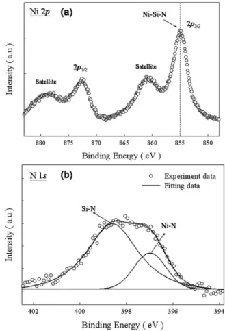
To further invetigate the nanocrystals, we have per-formed XPS analysis by using an Al K␣共1486.6 eV兲 x-ray radiation to demonstrate the chemical composition of the nanocrystals. To correct the possible charging effect of the film, the binding energy was calibrated using the C 1s 共284.6 eV兲 spectra of hydrocarbon that remained in the XPS analysis chamber as a contaminant. Figure 2共a兲 shows the XPS Ni 2p core-level photoemission spectra which consist of two main peaks, 2p3/2共⬃855 eV兲 and 2p1/2共⬃873 eV兲, with two small satellite peaks. According to the values of other literature, Ni 2p3/2 binding energies are at 852.3 and
853.4 eV for metallic nickel共Ni–Ni兲 and Ni silicide 共Ni–Si兲, respectively.15 However, it cannot be found that the above-mentioned peak signals are observed at the Ni 2p3/2peak by
XPS analysis. Due to the strong electronegativity of nitrogen atom, it is reasonably assumed that the larger Ni 2p3/2
bind-ing energy共⬃855 eV兲 of the nanocrystals can be assigned to Ni–Si–N ternary bond. This result is also supported by the XPS N 1s photoemission spectra, as shown in Fig.2共b兲. By the fitting result of binding energy, it is found that the main peak can be compose into two components which center at 398.5 and 397 eV corresponding to Si–N bond and Ni–N bond, respectively.16,17
For chemical characteristics of Si–N and Ni–N, the en-thalpies 共−⌬H兲 at room temperature are 470 and 70– 85 kJ mol−1, respectively.13,14 Hence, because of the higher enthalpy of Si–N compared with Ni–N, the N radicals can interact with Si atom easier than Ni atom during the sputtering process. It can be considered that a nitridation reaction will induce self-assembled phenomenon of NiSiN nanocrystal, as shown in Fig.1. In the previous research, Ni atom can diffuse in the SiNxeven at room temperature and
formation of a NiSiN ternary solid solution.18Therefore, the nanocrystals are simple and uniform to be formed at low
temperature by sputtering a comixed target in the Ar/ N2
en-vironment.
The typical capacitance-voltage 共C-V兲 hysteresis ob-tained with gate voltage from accumulation to inversion and in reverse is shown in Fig. 3. It is clearly observed that 1.5 and 3.5 V memory windows can be obtained under ±10 and ±12 V operations, respectively. The MOIOS structure with the NiSiN nanocrystals embedded in SiNxmatrix
exhib-its clear counterclockwise hysteresis by a flatband voltage shift共Vfb兲, indicating the significant memory effect. We
con-sider that the charges can be stored in both the NiSiN
nano-FIG. 1. Cross-sectional high resolution transmission electron microscope 共HRTEM兲 analysis of nitrogen incorporated Ni0.3Si0.7film between the
tun-nel oxide and the blocking oxide. The nanocrystal size and density are about 5 – 6 nm and 1.08⫻1012cm−2, respectively. The inset shows the memory
structure diagram.
FIG. 2. 共a兲 Ni 2p and 共b兲 N 1s x-ray photoelectron spectroscopy 共XPS兲 analyses of the nanocrystals. Empty circles and straight line indicate experi-mental and fitting results, respectively.
FIG. 3. Capacitance-voltage 共C-V兲 hysteresis of the fabricated MOIOS structure with the NiSiN nanocrystals embedded in SiNxmatrix as a charge trapping layer. The inset shows current density–voltage共J-V兲 characteristics.
082103-2 Chen et al. Appl. Phys. Lett. 91, 082103共2007兲
This article is copyrighted as indicated in the article. Reuse of AIP content is subject to the terms at: http://scitation.aip.org/termsconditions. Downloaded to IP: 140.113.38.11 On: Thu, 01 May 2014 00:10:12
crystal and the SiNx traps. Moreover, the hysteresis loops
follow the counterclockwise due to injection of electrons from the deep inversion layer and discharge of electrons from the deep accumulation layer of Si substrate. Hence, this memory window of NiSiN nanocrystals embedded in SiNx
matrix is enough to be defined 1 and 0 states. In addition, current density–voltage 共J-V兲 characteristics in the inset of Fig.3 show the current density of the MOIOS structure by gate voltage sweeping from 0 to 10 V and 0 to − 10 V. It is evident that the high quality of blocking oxide can avoid the stored carriers of charge trapping layer to leak into gate electrode.
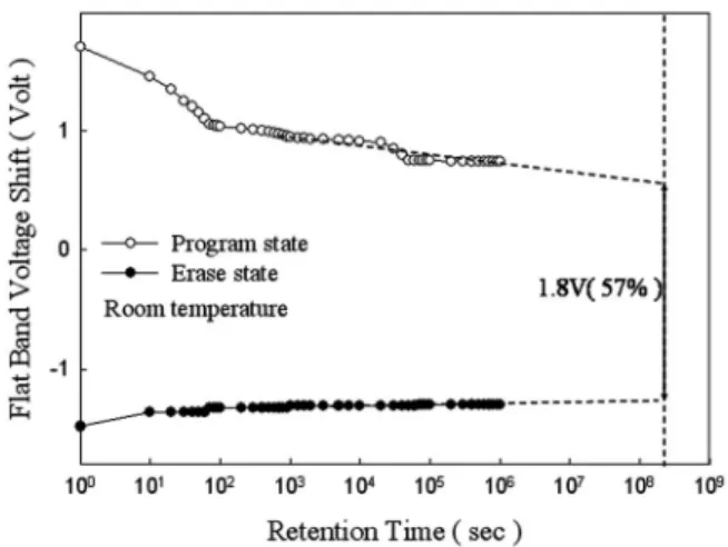
Retention characteristics of the memory structure with NiSiN nanocrystals are illustrated in Fig. 4. The retention measurements are performed at room temperature by operat-ing a ±10 V gate voltage stress for 5 s. The Vfbis obtained
by comparing the C-V curves from a charged state and a quasineutral state. When carriers are stored in the nanocrys-tals, the stored charges will raise the nanocrystal potential energy and increase the probability of escaping from the nanocrystal to the silicon substrate.19 Moreover, carriers trapped in the shallow traps are unstable and can easily leak back to the silicon substrate. It is found that the window of
Vfbsignificantly reduces during the first 1000 s and then
be-comes more stable for long retention time. This result is consistent with partial carrier trapping in the shallow trap state of the SiNxmatrix around the nanocrystals. However,
we use an extrapolation to give a long-term predictable result 共dotted line兲 after 1000 s 共stable region of retention兲 and ex-trapolate a memory window of 1.8 V共total charge hold ratio 57%兲 after 10 years. The majority carriers stored in the deep
trapping states of NiSiN nanocrystal surrounding with SiNx
matrix exhibit good retention characteristics.
In conclusion, the nonvolatile memory structure of Ni-SiN nanocrystals embedded in Ni-SiNxmatrix was fabricated by
sputtering a comixed target in the Ar/ N2 ambiance at room
temperature. A larger memory window of 3.5 V was ob-served after ±12 V voltage sweep for nonvolatile memory application. In addition, the date retention of the nanocrystal memory device is also good enough to maintain for 10 years. This work was performed at National Nano Device Laboratory and was supported by the National Science Council of the Republic of China under Contract Nos. NSC 2221-E-009-283, NSC 2221-E-009-270, NSC 95-2120-M-110-003, and NSC 95-2221-E-009-254-MY2. Fur-thermore, this work was partially supported by MOEA Tech-nology Development for Academia Project No. 94-EC-17-A-07-S1-046 and MOE ATU Program “Aim for the Top University” No. 95W803.
1S. Tiwari, F. Rana, K. Chan, H. Hanafi, W. Chan, and D. Buchanan,
Tech. Dig. - Int. Electron Devices Meet. 1995, 521.
2Y. C. King, T. J. King, and C. Hu, Tech. Dig. - Int. Electron Devices Meet.
1998, 115.
3J. D. Blauwe, IEEE Trans. Nanotechnol. 1, 72共2002兲.
4Z. Liu, C. Lee, V. Narayanan, G. Pei, and E. C. Kan, IEEE Trans. Electron
Devices 49, 9共2002兲.
5C. Lee, U. Ganguly, V. Narayanan, T. H. Hou, J. Kim, and E. C. Kan,
IEEE Electron Device Lett. 26, 12共2005兲.
6T. C. Chang, P. T. Liu, S. T. Yan, and S. M. Sze, Electrochem. Solid-State
Lett. 8, G71共2005兲.
7J. J. Lee, Y. Harada, J. W. Pyun, and D. L. Kwong, Appl. Phys. Lett. 86,
103505共2005兲.
8C. C. Wang, J. Y. Tseng, T. B. Wu, L. J. Wu, C. S. Liang, and J. M. Wu,
J. Appl. Phys. 99, 026102共2006兲.
9Ch. Sargentis, K. Giannakopoulos, A. Travlos, and D. Tsamakis, J. Phys.:
Conf. Ser. 10, 53共2005兲.
10D. Zhao, Y. Zhu, R. Li, and J. Liu, Solid-State Electron. 50, 2共2006兲. 11C. Lee, T. H. Hou, and E. C. Kan, IEEE Trans. Electron Devices 52, 12
共2005兲.
12C. H. Tu, T. C. Chang, P. T. Liu, H. C. Liu, S. M. Sze, and C. Y. Chang,
Appl. Phys. Lett. 89, 162105共2006兲.
13D. R. Lide, CRC Handbook of Chemistry and Physics, 81st ed.共CRC,
Boca Raton, FL, 2000兲, Vol. 81, p. 5-3.
14E. K. Parks, G. C. Nieman, K. P. Kerns, and S. J. Riley, J. Chem. Phys.
108, 3731共1998兲.
15C. D. Wagner, W. M. Riggs, L. E. Davis, J. F. Moulder, and G. E.
Muilenberg, Handbook of X-Ray Photoelectron Spectroscopy 共Perkin-Elmer, Eden Prairie, MN, 1975兲, p. 298.
16I. Crupi, D. Corso, G. Ammendola, S. Lombardo, C. Gerardi, B. DeSalvo,
G. Ghibaudo, E. Rimini, and M. Melanotte, IEEE Trans. Nanotechnol. 2, 4共2003兲.
17Y. Wang, Z. W. Fu, X. Li. Yue, and Q. Z. Qin, J. Electrochem. Soc. 151,
E162共2004兲.
18L. Aballe, L. Gregoratti, A. Barinov, M. Kiskinovaa, T. Clausen, S.
Gangopadhyay, and J. Falta, Appl. Phys. Lett. 84, 5031共2004兲.
19C. W. J. Beenakker, Phys. Rev. B 44, 1646共1991兲.
FIG. 4. Retention characteristics of the memory structure with NiSiN nano-crystals embedded in SiNxmatrix using a ±10 V gate voltage stress for 5 s at room temperature. The dotted line is the extrapolated value of retention data after 1000 s.
082103-3 Chen et al. Appl. Phys. Lett. 91, 082103共2007兲
This article is copyrighted as indicated in the article. Reuse of AIP content is subject to the terms at: http://scitation.aip.org/termsconditions. Downloaded to IP: 140.113.38.11 On: Thu, 01 May 2014 00:10:12