348 IEEE TRANSACTIONS ON ELECTRON DEVICES, VOL. 47, NO. 2, FEBRUARY 2000
A New Charge-Pumping Technique for Profiling
the Interface-States and Oxide-Trapped Charges in
MOSFET’s
Yu-lin Chu, Student Member, IEEE, Da-Wen Lin, and Ching-Yuan Wu, Member, IEEE
Abstract—A new charge-pumping method has been developed to characterize the hot-carrier induced local damages. By holding the rising and falling slopes of the gate pulse constant and then varying the high-level( GH) and base-level ( GL) voltages, the lateral distribution of interface-states( it( )) and oxide-trapped charges( ox( )) can be profiled. The experimental results show that during extracting ox( ) after hot-carrier stress, a contra-dictory result occurs between the extraction methods by varing the high-level( GH) and base-level ( GL) voltages. As a result, some modifications are made to eliminate the perturbation induced by the generated interface-states after hot-carrier stress for extracting
ox( ).
Index Terms—Charge-pumping method, interface-states, MOSFET, oxide-trapped charges.
I. INTRODUCTION
T
HE charge-pumping technique has become a powerful tool to quantitatively measure the energy and lateral distribu-tion of interface-states and the oxide-trapped charges [1]–[5], and has been utilized extensively to invesigate the hot carrier degradation induced by localized interface-states and the oxide-trapped charges [6], [7]. Some researchers [4], [8], [9] had as-sumed that the initial interface-states of a fresh device were uniformly distributed on the Si−SiO2 interface and theposi-tion of the interface-states generated by hot-carried stress could be easily extracted by some simple transformations. Actually, the initial interface-states are not necessary to be uniformly dis-tributed and hence these methods used to extract the damaged position might not be correct. In some other papers [9], [10], the “charge-neutralization” technique was used to compensate the stress-induced oxide-trapped charges, in which carriers of opposite polarity were injected into oxide layer to make the damaged region neutralized (i.e. hot-electron injection for hole traps and hot-hole injection for electron traps). It is extremely difficult to inject hot-carriers into the gate oxide without gen-erating extra interface-states. Therefore, the hot-carrier neutral-ization process may introduce errors and the accuracy of this technique is doubtful. In fact, it is well known that even no extra interface-states are generated by the hot-carrier neutralization
Manuscript received March 24, 1999; revised March 23, 1999. This work was supported by the National Science Council, Taiwan, R.O.C., under Contract NSC88-2215-E-009-039. The review of this paper was arranged by Editor M. Fukuma.
The authors are with the Advanced Semiconductor Device Research Labo-ratory and Institute of Electronics, National Chiao-Tung University, Hsinchu, Taiwan, R.O.C.
Publisher Item Identifier S 0018-9383(00)00688-2.
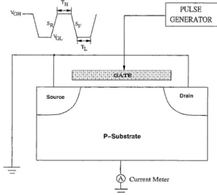
Fig. 1. Experimental setup of the charge-pumping measurement and the shape of the gate pulse.
process, the injected carriers are not stable and would leak away as time passed [11], [12]. Besides, charge-pumping measure-ment is very time-consuming, there is no way to ensure that the injected carriers would not leak away during charge-pumping measurement.
In this paper, a new charge-pumping technique for profiling both interface-states and oxide-trapped charges is presented, and some unreasonable assumptions are removed.
II. BASICPRINCIPLE
In this section, the basic principle of the charge-pumping technique is described, some questionable assumptions are dis-cussed, and the methods for further improvement are then made. The experimental setup for charge-pumping current measure-ment is shown in Fig. 1, where the gate pulse is provided by a HP 8110A pulse generator, and a HP 4145B parameter analyzer is used to monitor the charge-pumping current. In this work, the source/drain and substrate electrodes are always grounded to prevent any undesirable stress caused by measurement.
The charge-pumping current contributed by a local area can be written as
(1) where is the channel width, is the gate pulse frequency;, is the local interface-state density per area, and the
CHU et al.: PROFILING THE INTERFACE-STATES AND OXIDE-TRAPPED CHARGES IN MOSFET’S 349
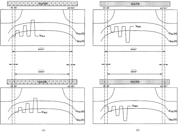
(a) (b)
Fig. 2. Illustration of the given gate-pulse voltage versus effective charge-pumping area for (a) base-level(V ) and (b) high-level (V ).
integration range from zero to gives the lateral length that can contribute to the charge-pumpint current. Note that only the region where the surface potential can fully swing from accumulation to inversion would provide the charge-pumping current. Based on this fact, the interface-states and the oxide-trapped charges on the Si−SiO2interface can be profiled.
The basic principle is described as follows. As shown in Fig. 2(a), the pulse generator gives a series of pulses with the base-level fixed at and high-level starting from a value slightly larger than to a fixed high-level to ensure that the charge-pumping current can reach its saturated value. After this step, the charge-pumping current attributed by the region between and can be measured. The result of is shown in Fig. 3. Again, a series of pulses with the base-level fixed at which is slightly larger than is generated, then the charge-pumping current attributed by the region between and can be measured. The result of is also shown in Fig. 3. Note that the differ-ence used to extract the interface-states and the oxide-trapped charges should not be too small, otherwise the noise induced by the measurement error will be serious. On the other hand, if the difference is large, the profiling resolution of interface-states and oxide-trapped charges will decrease. The difference between and is shown in
Fig. 3. Two charge-pumping currents with different base-levels and the difference between them.
Fig. 3, which is the charge-pumping current provided by the small region between and . behaves like a standard charge-pumping curve, which consists of a rising edge and a saturation region with the saturation value equal to . If the interface-states were generated after
350 IEEE TRANSACTIONS ON ELECTRON DEVICES, VOL. 47, NO. 2, FEBRUARY 2000
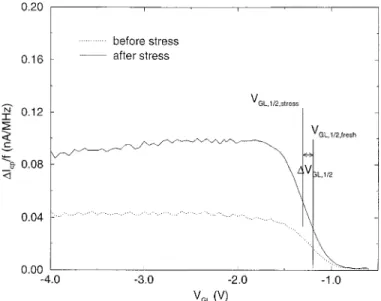
Fig. 4. Pre-stress and post-stress charge-pumping currents inside a small area defined by two different base-levels.
hot-carrier stress, the saturation level of would increase because there are more interface-states to produce the charge-pumping current. If the oxide-trapped charges were generated by hot-carrier stress, the rising edge of
would shift parallelly because the local threshold-voltage is changed by the oxide-trapped charges. If the polarity of the trapped charges is negative, the curve would shift to right because the local threshold-voltage increases. If the polarity of the oxide-trapped charges is positive, the curve would shift to left because the local threshold-voltage decreases. The half-maximum value of is chosen to be the reference point to measure the shift quantity [13], as shown in Fig. 4. Different base-levels of are related to different ranges where the potential can be biased into accumulation as the gate pulse stays low. This range is simulated by a two-dimensional (2–D) device simulator with a critical surface hole concentration
if inaccumulation
if not inaccumulation (2) where is the local hole concentration on the sil-icon surface. By comparing before and after stress, the total interface-states and the stress-induced oxide-trapped charges can be extracted by the following two equations:
(3) and
(4) where
(5) Similarly, the interface-states and the oxide-trapped charges can also be extracted by measuring the curves
Fig. 5. Two charge-pumping currents with different high-levels and the difference between them.
Fig. 6. Pre-stress and post-stress charge-pumping current inside a small area defined by two different high-levels.
under different high-levels of , as shown in Fig. 2(b). The typical and curves are shown in Fig. 5. It should be noted that during the measurement, the used should be smaller than the threshold-voltage so that the measured is mainly contributed by the re-gion near or inside the gate and drain overlapped area. Further-more, the curves and (the voltage shift related to half-maximum value of after stress) con-tributed by a local area near the drain junction from the differ-ence of two curves measured at different levels can be obtained, as shown in Fig. 6. It should be noted that the after stress slightly falls in lower , because the charge-pumping current difference contributed by a small area defined by two voltage levels of is very small (∼pA/MHz) even after stress and should be sensitive to the noise during measurement. Therefore, some measurement errors due to noise would result in a slight deviation from its saturated value. The rising edge of will shift to left for hole-traps and to right for electron-traps due to the change of
CHU et al.: PROFILING THE INTERFACE-STATES AND OXIDE-TRAPPED CHARGES IN MOSFET’S 351
local flat-band voltage. Note that different levels are re-lated to different ranges where the potential can be biased into inversion as the gate pulse stays high. This range can also be simulated by a 2–D device simulator with a critical surface elec-tron concentration
if ininversion
if not ininversion (6) where is the local electron concentration on the sil-icon surface. Also, the generated interface-states and the oxide-trapped charges should be written as
(7) and
(8) where
(9) In theory, both the magnitude and the position of and should be the same if and are correctly extracted while and would not be identical because the rising edge of both and curves would be perturbed by the generated interface-states after hot-carrier stress; that is, in (4) is underestimated for electron-traps and overestimated for hole-traps, and in (8) is overestimated for electron-traps and underestimated for hole-traps. Hence, the more reasonable method to extract the oxide-trapped charges should be modified and is described as follows.
and in (4) and (8) can be written as (10) and
(11) where is the shift value due to oxide-trapped charges, which is positive for hole-trap and is negative for electron-trap; is the absolute shift value due to generated interface-states after stress; and the subscripts “fresh” and “stress” mean the conditions before and after stress. Combining (10) and (11) gives
(12) Therefore, the oxide-trapped charges excluding the interfer-ence caused by the generated interface-states should be written as
(13) During profiling the interface-states and the oxide-trapped charges, the critical surface electron and hole concentrations must be carefully defined, otherwise the position of extracted in-terface-states and oxide-trapped charges may be incorrect. The
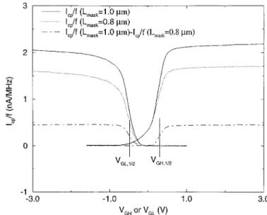
Fig. 7. I =f 0 V andI =f 0 V curves derived from the difference of two devices with different mask channel lengths.
methods for extracting and are described in the next sec-tion.
III. CRITICALSURFACEELECTRON ANDHOLECONCENTRATION
In our experiment, two devices with different mask lengths are needed to extract critical surface electron and hole concen-trations [13]. The mask lengths of the two devices are 1.0µm and 0.8µm, respectively. To extract the critical hole concentra-tion , the curve under a fixed high-level , which can make the entire channel inverted, is applied to the two devices. These two devices are identical except the mask length so that the charge-pumping current difference
of the two devices is mainly introduced by a small area inside the mid-channel region and the charge-pumping current con-tributed by the source/drain proximity effect can be ignored. The of the two devices is shown in Fig. 7, where corresponding to half-maximum of
is set to be the flat-band voltage of the mid-channel re-gion. is then put into a two-dimensional device simu-lator to simulate the surface hole concentraion. In our experi-ment, the simulated value is /cm3and hence we
de-fine /cm3. Similarly, a series of pulses with
a fixed base-level are applied to the two devices to ex-tract with the same procedure, the is also shown in Fig. 7, where corresponding to half-max-imum of is set to be the threshold-voltage of the mid-channel region. The simulated surface electron concen-traion at is /cm3and can be defined to be
/cm3.
IV. EXPERIMENTALRESULTS ANDDISCUSSION
Based on the aforementioned charge-pumping technique, the interface-states and the oxide-trapped charges generated by hot-carrier stress are measured. The test devices are LDD n-MOSFET’s with the mask channel length of 0.8 µm, the channel width of 120 µm and the oxide thickness of 110 Å, the device structure parameters used in 2-D device simulation
352 IEEE TRANSACTIONS ON ELECTRON DEVICES, VOL. 47, NO. 2, FEBRUARY 2000
Fig. 8. Distribution of the cumulative interface-states with the stress condition:
V = 7 V and V = 7 V.
are extracted by accurately simulating the curent-voltage (I-V) characteristics of the fresh device.
As described in Section II, the extraction procedures are sum-marized as follows.
1) Measure the and curves under various and conditions, respectively, then the and curves can be obtained. 2) Extract and from the and
curves, respectively.
3) Extract and from the charge-pumping current differ-ence and of the specified two short-channel devices, respectively.
4) Extract according to (3) and (7), and ac-cording to (12) and (13).
In our experiments, the curves are measured with varying from−2.4 V to−0.4 V and the
curves are measured with varying from−0.1 V to−1.7 V, and both the rising slope and the falling slope of the gate pulse are fixed to ensure that the charge-pumping currents are contributed by the same band-gap region. In our case, both
and of the gate pulse for measuring the and curves are set to be 2 V/µs.
In this work, the stress condition of V and
V, which may generate band-to-band tunneling(BTBT)-induced hot hole [14], [15], is taken for example. As shown in Fig. 8, the magnitude and the position of interface-states are very close for the extraction method under different base-levels of and high-levels of , this confirms the correct-ness of the extracted critical electron-surface concentration and hole-surface concentration . It also shows that the distribution of the interface-states for a fresh device is not uniform, this result contradicts the basic assumption of some previous papers [4], [8], [9]. Furthermore, as shown in Fig. 9, under different high-levels of and under different base-levels of are extracted, where the values of become smaller as the stress time incerases while the values of are nearly
Fig. 9. V andV extracted from1I =f 0V and
1I =f 0 V curves, respectively.
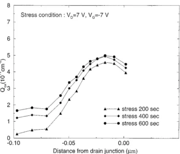
Fig. 10. distribution of the cumulative oxide-trapped charges with the stress condition:V = 7 V and V = 07 V.
invariant, this is contradictory if the hole-traps are generated after the BTBT-induced hot-hole stress. As a result, we can say that the extracted values of were perturbed by the generated interface-states so that the values of do not shift to a more negative value with cumulative stress time. Hence, (12) should be used to modify the contradictory results mentioned above and the extracted for different stress times are shown in Fig. 10. Note that as the surface potential under the gate/drain overlap region would be changed due to the generated interface-traps and oxide-trapped charges, the iteration process is necessary to obtain the accurate distribution, as mentioned in our previous work [5]. It should be noted that because the charge-pumping currents are very small for fresh devices, and in (12) are generated by 2-D numerical simulation instead of experimental results to prevent the measurement errors caused by noise. From Figs. 8 and 10, the maximum position of generated interface-traps is
CHU et al.: PROFILING THE INTERFACE-STATES AND OXIDE-TRAPPED CHARGES IN MOSFET’S 353
inconsistent with that of oxide-trapped charges. The phenom-enon is possible due to the fact that the generated electrons will travel toward the gate edge and the generated interface-traps are located near the gate edge; and the generated hole will travel away from the gate edge and the generated oxide-trapped charges are located away from the gate edge.
V. CONCLUSION
In this paper, the charge-pumping technique has been successfully applied to the characterization of stressd LDD n-MOSFET devices. In particular, a new method with mod-ifying the existing extraction technique of oxide-trapped charges is presented. By holding the rising and failing slopes of the gate pulse constant and then varying the high-level and base-level of the gate pulse, the smooth and curves related to a localized area near or inside the drain and gate overlapped region can be easily obtained, and the interface-states and oxide-trapped charges related to this area can be calculated at the same time. The experimental results obtained from and
curves during the extraction of after hot-carrier stress contradict to each other, and some unreasonable assumptions are removed to eliminate the interference induced by the generated interface-states after hot-carrier stress for extracting
.
REFERENCES
[1] G. Groeseneken, H. Maes, N. Beltran, and R. DeKeersmaecker, “A re-liable approach to charge-pumping measurements in MOS transistors,”
IEEE Trans. Electron Devices, vol. ED-31, p. 42, Jan. 1984.
[2] M. G. Ancona, N. S. Saks, and D. McCarthy, “Lateral distribution of hot-carrier-induced interface traps in MOSFET's,” IEEE Trans. Electron
Devices, vol. 35, p. 2221, Dec. 1988.
[3] W. Chen, A. Balasinski, and T. P. Ma, “Lateral profiling of oxide charge and interface traps near MOSFET junction,” IEEE Trans. Electron
De-vices, vol. 40, p. 187, Jan. 1993.
[4] M. Tsuchiaki, H. Hara, T. Morimoto, and H. Iwai, “A new charge pumping method for determining the spatial distribution of hot-car-rier-induced fixed charge in p-MOSFET's,” IEEE Trans. Electron
Devices, vol. 40, p. 1768, Oct. 1993.
[5] H. H. Li, Y. L. Chu, and C. Y. Wu, “A novel charge pumping method for extraction the lateral distribution of interface-trap and effective oxide-trapped charge densities in MOSFET devices,” IEEE Trans. Electron
Devices, vol. 44, p. 782, May 1997.
[6] A. Raychaudhuri et al., “Features and mechanisms of the saturating hot-carrier degradation in LDD NMOSFETs,” IEEE Trans. Electron
De-vices, vol. 43, p. 1114, July 1996.
[7] A. Bravaix et al., “Analysis of the hot-carrier degradation of deep-sub-micrometer large-angle-tilt-implanted drain(LATID) MOSFETs,” Solid
State Electron., vol. 41, p. 1293, Sept. 1997.
[8] W. K. Chim, S. E. Leang, and D. S. H. Chan, “Extraction of metal-oxide-semiconductor field-effect-transistor interface state and trapped charge spatial distributions using a physics-based algorithm,” J. Appl. Phys., vol. 81, p. 1992, Feb. 1997.
[9] C. Chen and T. P. Ma, “Direct lateral profiling of hot-carrier-induced oxide charge and interface traps in thin gate MOSFET's,” IEEE Trans.
Electron Devices, vol. 5, p. 512, Feb. 1998.
[10] D. S. Ang and C. H. Ling, “A novel experimental technique for the lat-eral profiling of oxide and interface state charges in hot-hole degraded
N-MOSFET's,” IEEE Electron Devices Lett., vol. 19, p. 23, Jan. 1998.
[11] T. Wang et al., “A new tenchique to measure an oxide trap density in a hot carrier stressedn-MOSFET,” in IEDM Tech. Dig., 1997, p. 292. [12] T. Wang, T. E. Chang, L. P. Chiang, C. H. Wang, N. K. Zous, and C.
Huang, “Investigation of oxide charge trapping and detrapping in a MOSFET by using a GIDL current technique,” IEEE Trans. Electron
Devices, vol. 45, p. 1511, July 1998.
[13] H. H. Li and C. Y. Wu, “A novel extraction technique for the effective channel length of MOSFET devices,” IEEE Trans. Electron Devices, vol. 42, p. 856, May 1995.
[14] C. Chang, S. Haddad, B. Swaminathan, and J. Lien, “Drain-Avalanche and hole trapping induced gate leakage in thin-oxide MOS devices,”
IEEE Electron Devices Lett., vol. 9, p. 588, Nov. 1988.
[15] Y. Igura, H. Matsuoka, and E. Takeda, “New device degradation due to ‘cold’ carriers created by band-to-band tunneling,” IEEE Electron
De-vices Lett., vol. 10, p. 227, May 1989.
Yu-Lin Chu (S’91) was born in Taiwan, R.O.C., on
September 10, 1968. He received the B.S. degree from the Department of Material Science and En-gineering, National Tsing-Hua University, Taiwan, in 1991, and the M.S. degree from the Institute of Electronics, National Chiao-Tung University, Hsinchu, Taiwan, in 1993. He is currently pursuing the Ph.D. degree at the same institute.
His present research areas focus on deep-submi-crometer MOS device physics and reliability issues.
Da-Wen Lin was born in Taiwan, R.O.C., on
February 10, 1974. He received the B.S. degree from the Department of Electronics Engineering, National Chiao-Tung University (NCTU), Hsinchu, Taiwan, in 1996, and the M.S. degree from the Institute of Electronics, NCTU, in 1998.
He is currently in military service as a second Lieu-tenant. His research interest is in the modeling and physics of MOSFET reliability.
Mr. Lin is a member of Phi Tau Phi.
Ching-Yuan Wu (S'72-M'75) was born in Taiwan,
R.O.C., on March 18, 1946. He received the B.S. degree in electrical engineering from the National Taiwan University, Taipei, in 1968, and the M.S. and Ph.D. degrees from the State University of New York (SUNY), Stony Brook, in 1970 and 1972, respectively.
During the 1972–1973 academic year, he was a Lecturer in the Department of Electronical Sciences, SUNY. During the 1973–1975 academic years, he was a Visiting Associate Professor at the National Chiao-Tung University (NCTU), Hsinchu, Taiwan. In 1976, he became Full Professor in the Department of Electronics and the Institute of Electronics at NCTU. While there, he was Director of the Engineering Laboratories and Semiconductor Research Center from 1974 to 1980, the Director of the Institute of Electronics from 1978 to 1984, and the Dean of the College of Engineering from 1984 to 1990. He was a Principal Investigator of the National Electronics Mass Plan-Semiconductor Devices and Integrated-Circuit Technologies from 1976 to 1979, and had been a Coordinator of the National Microelectronics Research and High-Level Man-Power Education Committee, National Science Council, Taiwan, from 1982 to 1988. He has been the Research Consultant of the Electronics Research and Service Organization (ERSO), ITRI, a member of the Academic Review Committee in the Ministry of Education, and the Chairman of the Technical Review Committee on Information and Microelec-tronics Technologies, Ministry of Economic Affairs. His research activities have been in semiconductor device physics and modeling, and integrated circuit designs and technologies. His current work focuses on the development of efficient 2-D and 3-D simulators for deep-submicrometer CMOS devices. He has published over 180 papers in the semiconductor field and has served as a reviewer for international journals such as IEEE ELECTRONDEVICELETTERS, IEEE TRANSACTIONS ONELECTRONDEVICES,and Solid-State Electronics.
Dr. Wu is a member of the Honorary Editorial Advisory Board of Solid-State
Electronics, and is a board member of the Chinese Engineering Society. He
re-ceived the Academic Research Award in Engineering from the Ministry of Edu-cation in 1979 and the Outstanding Scholar Award from the Chinese EduEdu-cational and Cultural Foundation in 1985. He received the Outstanding Research Pro-fessor Fellowship from the Ministry of Education and National Science Council from 1982 to 1999. He received the Distinguished Engineering Professor Medal Award from the Chinese Engineering Society in 1992.