IEEE TRANSACTIONS ON MAGNETICS, VOL. 47, NO. 3, MARCH 2011 633
Effect of Top Electrode Materials on the Nonvolatile Resistive Switching
Characteristics of CCTO Films
Chun-Chieh Lin
1, Yi-Peng Chang
1, Chia-Cheng Ho
2, Yu-Shu Shen
3, and Bi-Shiou Chiou
3 Department of Electrical Engineering, National Dong Hwa University, Hualien 974, TaiwanR&D Department, Taiwan Semiconductor Manufacturing Company, Hsinchu 300, Taiwan Institute of Electronics, National Chiao Tung University, Hsinchu 300, Taiwan
A novel material CaCu3Ti4O12 (CCTO) for resistive random access memory (RRAM) application was prepared by sol-gel spin-coating method. Our previous studies indicated that the CCTO possesses stable resistive switching behavior. In this work, the effects of the top electrode (TE) material on the resistive switching characteristics of CCTO films are investigated. It indicates the work function of the TE is an important factor on the resistive switching properties. Successive resistive switching was observed for electrode materials of Ni, Pd, and Pt. Furthermore, optimized consideration of the electrode material for RRAM is also studied.
Index Terms—Electrodes, nonvolatile memory, resistive random access memory, work function.
I. INTRODUCTION
N
EW technologies for making next-generation nonvolatile memory (NVM) have attracted extensive attention due to the conventional memory approaching its scaling limits. The re-quirements for the next-generation NVM include high speed, high-density integration, and low power consumption [1]–[6]. In recent years, more attention has been paid to the develop-ment of resistive random access memory (RRAM), which is one of the promising candidates for the next-generation NVM appli-cation due to its superior properties, such as reversible resistive switching, simple structure, small size, low power consumption, high operation speed, and low cost [7].Recently, research efforts have been focused on the effects of the electrode materials on the resistive switching properties [8], [9]. These studies indicate that contacts between the electrode material and resistive film are related to the resistive switching behavior. In the case of the p-type oxide, electrode material with large work function causes an Ohmic contact or a low Schottky barrier to induce the resistive switching behavior. However, how to optimize the RRAM properties such as memory window, en-durance, and currents forONandOFFstates has not been clarified extensively.
Our previous work on CaCu Ti O (CCTO) deposited by sol-gel spin-coating method shows crystallinity and uniform mi-crostructure [10]–[12]. The CCTO also has excellent resistive switching properties and a small degradation of current ratio between the ON andOFFstates. In this work, electrode mate-rial dependence on resistive switching properties of the CCTO films are investigated, and optimized consideration for RRAM applications has also been explored.
II. EXPERIMENTALPROCEDURE
The precursor solution of the CCTO was prepared by dis-solving the appropriate ratio of calcium and cupric acetates in acetic acid, and then a stoichiometric amount of titanium (IV) isopropoxide was added into the solution. In order to increase Manuscript received August 26, 2010; revised December 06, 2010; accepted December 14, 2010. Date of current version March 02, 2011. Corresponding author: C.-C. Lin (e-mail: [email protected]).
Color versions of one or more of the figures in this paper are available online at http://ieeexplore.ieee.org.
Digital Object Identifier 10.1109/TMAG.2010.2101584
the solution stability, ethylene glycol was also added into the precursor solution. After that, the formamide was selected as an additive to adjust the solution viscosity to prevent from cracking of the CCTO films during drying and baking. The precursor so-lution was then heated at 100 C for 1.5 h to ensure a complete reaction [12].
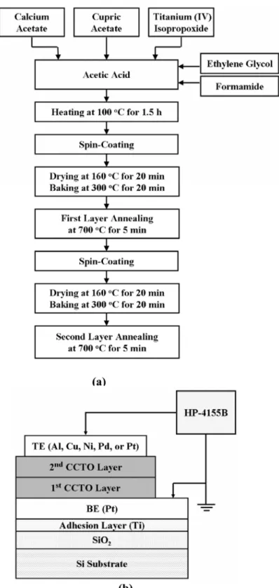
Metal-resistor-metal structure with the top electrode (TE)/CCTO/Pt/Ti/SiO /Si was employed in this work. Ini-tially, the boron-doped p-type (100) Si wafer was adopted as a substrate for device fabrication. After performing the standard Radio Corporation of America (RCA) cleaning process, a 100-nm-thick SiO was grown on the Si substrate by oxidation furnace. 5-nm-thick Ti and 50-nm-thick Pt, serving as the adhesion layer and bottom electrode (BE), respectively, were continuously deposited on the SiO by dc sputtering without breaking a vacuum. The CCTO film was deposited on the Pt/Ti/SiO /Si substrate by a two-stage spin-coating process. The first spin-coated layer was baked at 160 C for 20 min for drying the gel; then it was baked at 300 C for 20 min for removing the residual organic compounds. The sample was then annealed at 700 C for 5 min in atmosphere. The second CCTO layer was also deposited by spin-coating method on the first CCTO layer directly. The baking and annealing processes of the second CCTO layer were performed as those of the first one. Two layers of CCTO film were spin-coated sequentially in order to avoid through pin-holes [10]. Fig. 1(a) and (b) show the fabrication flow chart of the CCTO film by the sol-gel spin-coating method, and the schematic structure of the CCTO-based RRAM device, respectively. The total thickness of two CCTO layers was about 250 nm [12]. Finally, the TEs of Al, Cu, Ni, Pd, and Pt were deposited on the samples by dc sputtering at room temperature (RT) through a shadow mask. A semiconductor parameter analyzer (HP-4155B) was used to measure the current-voltage (I-V) characteristics of the CCTO-based RRAM devices. During the measurement, the bias voltage was applied on TE with grounded Pt BE. In addition, all the measurements were performed at RT.
III. RESULTS ANDDISCUSSION
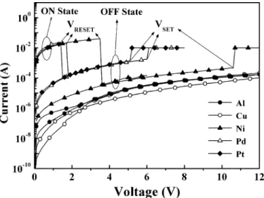
Fig. 2 depicts the typical resistive switching I-V curves of the CCTO-based RRAM devices with various TEs, including Al, Cu, Ni, Pd, and Pt. Before the resistive switching is performed, 0018-9464/$26.00 © 2011 IEEE
634 IEEE TRANSACTIONS ON MAGNETICS, VOL. 47, NO. 3, MARCH 2011
Fig. 1. (a) Fabrication flow chart of the CCTO film by the sol-gel spin-coating method. (b) The schematic structure of the CCTO-based RRAM device [12]. a forming process achieved by applying dc voltage is necessary.
After the forming process, a high conductive state (ONstate) is obtained, and then the device holds on theONstate. By applying the voltage bias to , the device is switched from the ON state to anOFFstate, called as turn-off process. Then, the device can keep at theOFFstate until is applied on TE. The current abruptly increases, and the device is switched back to the ONstate, called as turn-on process. A current compliance is set at 10 mA during the forming and turn-on processes to prevent the permanent damage on the CCTO film. However, no current
compliance is used during the turn-off process; therefore, theON state current could be over 10 mA. As shown in Fig. 2, two distinct resistance states, i.e., resistive switching, are observed in the TEs of Pt, Pd, and Ni, but no resistive switching is exhibited for the TEs of Cu and Al.
As the CCTO-based RRAM devices went through many resistive switching cycles, the memory window (current ratio between theON andOFFstates) indicates the endurance char-acteristics. In this work, the endurance of the CCTO-based RRAM devices is measured in terms of the number of resistive
LIN et al.: NONVOLATILE RESISTIVE SWITCHING CHARACTERISTICS OF CCTO FILMS 635
TABLE I
RESISTIVESWITCHINGPROPERTIES OF THECCTO-BASEDRRAM DEVICES AND THEWORKFUNCTIONS OFVARIOUSTES
Fig. 2. Typical resistive switching I-V curves of the CCTO-based RRAM de-vices with various TEs.
Fig. 3. The currents versus the resistive switching cycles of the CCTO-based RRAM devices. Difference between theI andI is referred to as the memory window.
switching cycles, and the memory window is maintained above 10 times to avoid readout errors and noise effects [13]. Fig. 3 exhibits the currents at 0.3 V of both ONandOFFstates. The
specimens of TEs of Pt, Pd, and Ni are entirely reversible and reproducible during the successfully resistive switching cycles. The CCTO-based RRAM device with a TE of Ni shows the largest ratio between the and theOFFstate current . The ratios of the CCTO-based RRAM device with the Ni TE at the 1st and 100th resistive switching cycles are 51140 and 5190, respectively. Table I summarizes the current ratios between theONandOFFstates for all specimens. All the CCTO-based RRAM devices show a large memory window, and the ratios between and remain above 100 times, which is fea-sible to distinguish between theONandOFFstates to avoid the readout errors and noise effects. The drastic resistance change from the OFFstate to the ON state is attributed, according to our previous report [12], to the establishment of the conductive paths. Many conductive paths are connected in parallel between the TE and BE in theONstate. is dependent on the amount of conductive paths between the TE and BE. Hence, similar is obtained for the specimens of TEs of Ni, Pd, and Pt, as shown in Fig. 3.
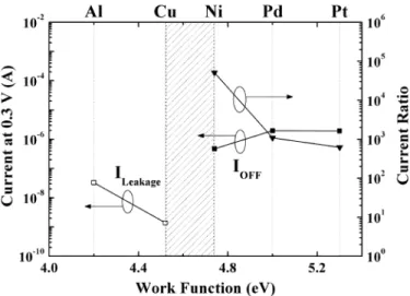
Fig. 4 shows the currents and current ratios between and of the 1st switching cycle, while a read voltage of 0.3 V is applied. Regarding the specimens of TEs of Pt, Pd, and Ni, the currents at theOFF state are higher than the leakage current of TEs of Cu and Al. According to the Schottky con-tact model, the characteristics of the metal-semiconductor junc-tion are determined by the metal work funcjunc-tion and the Fermi level in the semiconductor. Joanni et al. indicated that CCTO thin films exhibit p-type semiconductor behavior [14]. There-fore, the junction made from TE with large work function con-tacting the CCTO film exhibits an Ohmic contact. The work functions of TE materials are also summarized in Table I. Pt, Pd, or Ni with larger work functions form an Ohmic contact or a low Schottky barrier with the CCTO film. Consequently, higher voltages across the CCTO film are required to induce enough current at theOFFstate to establish the conductive paths. Then, the CCTO film can be switched from theOFFstate to theON state. For the specimen with TE of Al or Cu with the smaller work function, a high Schottky barrier is formed at the interface between the TE and the CCTO. The leakage current through CCTO film in this case is not enough to establish the conduc-tive paths and to induce the resisconduc-tive switching. Therefore, no resistive switching is observed in the specimen with TEs of Al and Cu. It is reasonable to conclude that the resistive switching
636 IEEE TRANSACTIONS ON MAGNETICS, VOL. 47, NO. 3, MARCH 2011
Fig. 4. TheI and the ratio betweenI andI at 0.3 V as a function of the work function of TE. No resistive switching is observed for the specimens of TEs of Al and Cu. Therefore, no current ratio is obtained, and the leakage currents are only indicated.
of the CCTO film is obtained only with the electrode material with larger work function.
However, even though the electrode with the larger work function induces the resistive switching in CCTO, it also causes a decrease in the current ratio and degrades the memory
window between and of the CCTO-based RRAM,
as shown in Fig. 4. It leads us into further consideration of the optimum electrode work function. First of all, the work function plays a key role in determining , and is also important to maximize the ratio between and , i.e., the ratio must be appreciable to distinguish between the and to avoid readout errors and noise effects. For the TE materials investigated in this study, Ni appears to be the optimized TE for the CCTO film. It provides the appropriate work function to achieve the resistive switching characteristics with about 51140
times memory window between the and .
As mentioned above, the TE material with the larger work function can induce more current through the CCTO film and cause the resistive switching. Subjected to stability and compat-ibility requirements for TE materials, it is possible to conclude that to induce an enough current for the resistive switching be-havior to occur, a TE with work function greater than 4.5 eV is needed. Thus, for copper with work function of 4.5 eV, no re-sistive switching was exhibited on the Cu/CCTO/Pt structured device. In addition, when the work function of TE material is smaller, lower is also obtained. On the other hand, higher ratio between and than that of the Ni/CCTO/Pt struc-tured device is suggested, as the work function is smaller than 4.7 eV. Judged from the above, we suggest that a work function of the optimized TE material probably exists within the shaded area shown in Fig. 4.
IV. CONCLUSION
In summary, the effects of TE materials on the resistive switching characteristics of CCTO films are investigated in this work. It is found that the devices with Pt/CCTO/Pt, Pd/CCTO/Pt, and Ni/CCTO/Pt structures exhibit the resistive switching behavior. It is believed that the main reason is that low Schottky or Ohmic contact between the TE and CCTO
film induces an effective voltage drop inside the CCTO film, and then leads to the formation of conductive paths. Among the TE materials of Pt, Pd, and Ni, the work function of Ni is the lowest one. Consequently, Ni/CCTO/Pt structured device exhibits the lowest , and has the largest ratio between and . Regarding the Ni/CCTO/Pt structured device, not only the resistive switching characteristics are obtained, but the excellent memory window is exhibited. Given that the stability and compatibility requirements for the CCTO process, the optimized work function of the TE material was also indicated. Finally, the points of optimized TE materials made in this study can also apply in principle to other RRAM materials.
ACKNOWLEDGMENT
This work was supported by the National Science Council of Taiwan under project number NSC 98-2221-E-259-029.
REFERENCES
[1] M. Fujimoto, H. Koyama, S. Kobayashi, Y. Tamai, N. Awaya, Y. Nishi, and T. Suzuki, “Resistivity and resistive switching properties of Pr Ca MnO thin films,” Appl. Phys. Lett., vol. 89, 2006, # 243504.
[2] C.-C. Lin, C.-Y. Lin, M.-H. Lin, C.-H. Lin, and T.-Y. Tseng, “Voltage-polarity-independent and high-speed resistive switching properties of V-doped SrZrO thin films,” IEEE Trans. Electron Devices, vol. 54, no. 12, pp. 3146–3151, Dec. 2007.
[3] C.-Y. Lin, C.-Y. Wu, C.-Y. Wu, and T.-Y. Tseng, “Modified resistive switching behavior of ZrO memory films based on the interface layer formed by using Ti top electrode,” J. Appl. Phys., vol. 102, 2007, # 094101.
[4] C.-Y. Lin, S.-Y. Wang, D.-Y. Lee, and T.-Y. Tseng, “Electrical prop-erties and fatigue behaviors of ZrO resistive switching thin films,” J.
Electrochem. Soc., vol. 155, no. 8, pp. H615–H619, 2008.
[5] W. Zhao, E. Belhaire, C. Chappert, and P. Mazoyer, “Power and area optimization for run-time reconfiguration system on programmable chip based on magnetic random access memory,” IEEE Trans. Magn., vol. 45, no. 2, pp. 776–780, Feb. 2009.
[6] W. Wang, “Magnetic random accessible memory based magnetic con-tent addressable memory cell design,” IEEE Trans. Magn., vol. 46, no. 6, pp. 1967–1970, Jun. 2010.
[7] I. G. Baek, M. S. Lee, S. Seo, M. J. Lee, D. H. Seo, D.-S. Suh, J. C. Park, S. O. Park, H. S. Kim, I. K. Yoo, U.-I. Chung, and J. T. Moon, “Highly scalable non-volatile resistive memory using simple binary oxide driven by asymmetric unipolar voltage pulses,” in IEDM Tech.
Dig., 2004, pp. 587–590.
[8] W.-Y. Yang and S.-W. Rhee, “Effect of electrode material on the re-sistance switching of Cu O film,” Appl. Phys. Lett., vol. 91, 2007, # 232907.
[9] W.-G. Kim and S.-W. Rhee, “Effect of the top electrode material on the resistive switching of TiO thin film,” Microelectron. Eng., vol. 87, pp. 98–103, 2010.
[10] L.-C. Chang, D.-Y. Lee, C.-C. Ho, and B.-S. Chiou, “Thickness-depen-dent microstructures and electrical properties of CaCu Ti O films derived from sol-gel process,” Thin Solid Films, vol. 516, pp. 454–459, 2007.
[11] Y.-S. Shen, B.-S. Chiou, and C.-C. Ho, “Effect of annealing tempera-ture on the resistance switching behavior of CaCu Ti O ,” Thin Solid
Films, vol. 517, pp. 1209–1213, 2008.
[12] Y.-S. Shen, C.-C. Ho, and B.-S. Chiou, “Impedance spectroscopy of CaCu Ti O films showing resistive switching,” J. Electrochem.
Soc., vol. 156, no. 6, pp. H466–H470, 2009.
[13] K. P. Biju, X. Liu, E. M. Bourim, I. Kim, S. Jung, M. Siddik, J. Lee, and H. Hwang, “Asymmetric bipolar resistive switching in solution-processed Pt/TiO /W devices,” J. Phys. D-Appl. Phys., vol. 43, 2010, # 495104.
[14] E. Joanni, R. Savu, P. R. Bueno, E. Longo, and J. A. Varela, “P-type semiconductor gas sensing behavior of nanoporous rf sputtered CaCu Ti O thin films,” Appl. Phys. Lett., vol. 92, 2008, # 132110. [15] B. Pellegrini, “Properties of silicon-metal contacts versus metal
work-function silicon impurity concentration and bias voltage,” J.