Growth and Physical Characterization of Polygon
Prismatic Hollow Zn-ZnO Crystals
Kun-Ho Liu, Chin-Ching Lin, and San-Yuan Chen*
Department of Materials Science and Engineering, National Chiao Tung University, 1001 Ta-hsueh Road, Hsinchu, Taiwan
Received June 9, 2004; Revised Manuscript Received November 4, 2004
ABSTRACT: A hierarchical polygon prismatic Zn-ZnO core-shell structure was grown on silicon by combining liquid-solution colloidals together with the vapor-gas growth process. Zn colloidals with a diameter of 5-10 nm synthesized from Zn(ClO4)2precursor solution were used as nucleation seeds for the growth of Zn polygon prismatic
nanocrystals. Depending on carrier gas and annealing conditions, the polygon prismatic Zn crystals having morphology from hollow to dense configuration can be manipulated. Moreover, after prolonged thermal treatment at 300-400 °C, polygon prismatic hollow ZnO-Zn crystals with a dimension from nanometer to micrometer can be obtained. The room-temperature photoluminescence spectra show that the hollow ZnO-Zn crystals have a weak ultraviolet (UV) emission at 380 nm and a strong green emission at 500 nm. However, the intensity of the UV emission can be improved by postannealing the Zn-ZnO core-shell structure in an oxygen atmosphere to form hollow ZnO crystals.
Introduction
The zinc oxide (ZnO) nanostructure is one of the most promising materials for optoelectronic applications, including photodetectors,1solar cells,2,and nanolasers3
because it possesses a direct band gap of 3.37 eV and strong exciton binding energy of 60 meV which can ensure an efficient exciton emission at room tempera-ture.
During the past few years, many different morpho-logical ZnO nanostructures, including nanowires,4
na-norods,5nanocables,6and nanobelts,7have been
fabri-cated. Moreover, various techniques such as thermal decomposition,8 vapor-phase transport,9 and
metal-organic chemical vapor deposition (MOCVD)10 have
been developed to synthesize ZnO nanostructures. The vapor-liquid-solid (VLS) method is a common ap-proach to grow nanostructures, and many researchers have tried to control the process parameters to produce nanocrystals of technologically useful geometry.11,12
Many efforts have been successfully invested in the growth of ZnO nanorods or nanowires. However, this method has been based on high-temperature processing. On the other hand, although liquid-phase chemical synthesis can be also used to grow nanorods at a lower temperature, different anisotropic shapes of nanocrys-tals have been limited. So far, only rod-based morphol-ogy has been obtained.
One of the challenges in materials is to control the structure of materials on specific nanomorphologies.13,14
Especially, both controlled shape and size of inorganic nanocrystals have a strong influence on electrical and optical properties.15,16In the past, Yamada et al.
devel-oped ZnO fine crystals with various growth forms by rapid condensation of the high-temperature ultrasuper-saturated gas generated from ZnO powder by means of the conically converging shock-wave technique in 1989.17
Recently, it was reported that ZnO and beltlike Zn particles can be synthesized via thermolysis of the
molecular precursors [MeZnOSiMe3]4and [Zn(OSiMe3)2]n in the temperature range of 160-500 °C.18Obviously,
several metal-organic precursors in the solid state and/ or solution can be used for the synthesis of Zn- and/or nanocrystalline ZnO particles.
In contrast to conventional processes, a novel process was proposed to combine the aforementioned vapor-gas with liquid-solution methods for growing polygon prismatic Zn and ZnO crystals with a dimension from nanometer to micrometer. The liquid-solution method supplies the uniform nanoseeds to serve as nuclei, and the subsequent vapor-gas-phase process provides the Zn source for the growth of Zn or ZnO crystals.
Furthermore, it was found that depending on growth conditions such as temperature, time, and atmosphere, dense and hollow polygon prismatic Zn crystals can be developed.19Therefore, both physical characterization
and photoluminescence properties of the polygon pris-matic hollow Zn-ZnO crystals will be investigated in this work.
Experimental Methods
Polygon prismatic ZnO and Zn nanocrystals were synthe-sized using colloidal Zn particles and a physical vapor trans-port system. The colloidal Zn prepared in methanol with 50 mL of 10-2 M Zn(ClO
4)2solution was added to 442 mL of methanol plus 8 mL of 5 M NaOH and left for 24 h overnight. A transparent solution was finally obtained with its light absorption starting at 350 nm. In this work, ZnO and graphite powders were used for the growth source of Zn nanocrystals and ball-mixed in ethanol for 15 h. An alumina tube was mounted inside a high-temperature tube furnace with the source material placed on an alumina boat and positioned at the center of the alumina tube. Subsequently, the Si substrate was spin-coated with various concentrations of the colloidal Zn and then located downstream of the carrier gas flow in the alumina tube where the tube was sealed and evacuated by a mechanical rotary pump to a pressure of 80 mTorr. High-purity Ar was used as the carrier gas with a flow rate of 10 sccm, and the reaction was carried out at 1100 °C for 0.5-5 h to form polygon prismatic hollow Zn crystals at the substrate temperatures of 300-400 °C. The temperature in both tem-perature zones was measured and corrected with K-type
* To whom correspondence should be addressed. Tel:+ 886-3-5731818. Fax: +886-3-5725490. E-mail: [email protected].
CRYSTAL
GROWTH
& DESIGN
2005
VOL. 5, NO. 2
483-487
10.1021/cg0498150 CCC: $30.25 © 2005 American Chemical Society Published on Web 12/30/2004
thermocouples. The data error was about 5-10 °C. After thermal treatment, the Zn polygon prismatic nanocrystals were taken out and then annealed at 350 °C in a pure oxygen atmosphere (5 N) for different periods of time to form ZnO on the surface of the Zn hollow crystals. For comparison, a mixture gas of Ar and oxygen was also used for the crystal growth.
The deposited material was analyzed by field emission scanning electron microscopy (FE-SEM, S-4100), and the crystal structure was determined using X-ray diffraction (XRD, Siemens D5000). The depth profile of polygon prismatic ZnO-Zn crystals was measured using AES (Auger nanoprobe electron spectroscopy, Auger 670 PHI Xi). Transmission electron microscopy (TEM, Philips TECNAI 20) with energy-dispersive X-ray spectroscopy (EDS) operated at 200 keV was also used for structural analysis. Photoluminescence measure-ment was performed by excitation from a 325 nm He-Cd laser at room temperature.
Results and Discussion
Figure 1 shows the typical SEM and TEM images of the polygon prismatic Zn nanocrystals as a function of growth time at 300 °C. In an initial growth stage (<0.5 h), many nanoparticles with particle size smaller than 30 nm were identified and are shown in Figure 1a. When the growth time is extended over 30 min (0.5 h), those nanoparticles are gradually agglomerated to-gether to form a polygon-based shape as shown in Figure 1b that is close to the composing-crystals shown in the inset of Figure 1b with a diameter around 150 nm. Later, a stable compact structure of polygon pris-matic Zn nanocrystals was developed in Figure 1c. According to our previous studies, the nucleation size of the polygon prismatic crystals is related to the concentration of the Zn(ClO4)2 solution. As a higher
colloidal concentration was used, the agglomerate de-gree among the nanoparticles was apparently increased. Furthermore, a larger number of agglomerate regions with a bigger size of the structure by self-assembly of Zn nanocrystals were observed.19The diameter of the
polygon Zn crystals can be tuned from 100 nm to 1 µm by simply varying the growth temperature and time. However, the growth mechanism of the crystals is not the focus of this work and will be reported elsewhere.20
When the growth time exceeds 3 h, it was found that anisotropic structures such as wires and rods were grown on the surface of the crystals, as shown in Figure 1d. In addition, the surface became rough and many pores were formed on the surface. This observation suggests that above a critical growth time, many defects would be created on the surface of polygon prismatic crystals because zinc metal becomes unstable and sublimated in an Ar atmosphere. Then, the defects could act as nucleation sites to grow anisotropic structure because of the cavitation effect.
On the other hand, as the sample was treated at 350 °C, Figure 2a shows that the polygon-based Zn crystals were rapidly developed in an initial growth stage (t < 0.5 h), but with porous structure formed inside the crystals. With increasing growth time up to 2 h, Figure 2b indicates that the polygon prismatic Zn crystals with a hollow structure have been formed. However, the polygon prismatic structure becomes unstable and tends to form spherelike morphology as the growth time exceeds 3 h. The formation mechanism for both compact and hollow polygon prismatic Zn structure is given in ref 20 and is briefly described as follows. After the Zn-(ClO4)2solution containing Zn colloidals was deposited
on the Si substrate, these nuclei would cap these Zn molecules to develop the nanocrystals when Zn sources were transported by a thermal evaporation process. Moreover, Zn nanocrystals would be assembled by attractive force to form a base of polygon prismatic crystals and organized in a compact hexagonal network. At a lower temperature below 300 °C, a compact polygon prismatic Zn crystal was maintained due to solidifica-tion of liquid droplets. However, as the sample was treated at 300-400 °C in Ar, sublimation of the Zn core and surface oxidation of the Zn crystal would result in the formation of a hollow structure. If a higher growth temperature, i.e., 500 °C, was used, the whole structure almost collapsed (not shown here) because the melting point of Zn is about 410 °C.
Figure 3 shows the X-ray diffraction spectra of the Zn crystals. As the sample was grown in pure argon at 350 °C for 2 h, Figure 3a illustrates that only Zn phase can be detected from the polygon prismatic hollow Zn crystals. When the Zn crystals were then postannealed at the same temperature (350 °C) for 2 h in an oxygen atmosphere without Zn source supplied, it was found that zinc oxide was developed from the polygon pris-matic hollow crystals as evidenced in the XRD pattern of Figure 3b. Furthermore, prolonged oxygen annealing of 30 h at 350 °C promotes the formation of ZnO. As evidenced in Figure 3c, only ZnO phase and an almost negligible Zn peak are observed, indicating that the polygon prismatic hollow Zn crystals were nearly oxi-dized into ZnO. A similar transformation from Zn into ZnO was also reported in the literature.21 Li et al.
treated Zn nanowires grown by the anodic alumina oxide (AAO) process in air at 300 °C for 35 h and found that ZnO nanowires could be formed.
During our systematical exploration of the formation process of Zn-ZnO crystals, it seems that there exists Figure 1. Morphology development of polygon prismatic
compact Zn crystals as a function of growth time at 300 °C in an Ar atmosphere. (a) TEM image of polygon prismatic Zn nanoparticles (<30 nm) formed by the thermal vapor process in the initial growth stage. (b) Polygon prismatic Zn clusters are attracted together in 0.5 h and arranged into a polygon-based shape (inset). Also shown is the morphology of polygon prismatic Zn crystals in (c) 2 h and (d) 4 h.
a transition temperature around 300-350 °C from compact to hollow structure for the Zn crystals grown in an Ar atmosphere. Different structural morphologies of the Zn-ZnO crystals can be achieved by carefully controlling the growth temperature and atmosphere. Furthermore, as the crystals were grown at 320 °C for 2 h in Ar atmospheres, it was found that the Zn crystals exhibit compact structure with a morphology similar to that grown at 300 °C. However, as analyzed by AES where a polygon prismatic Zn crystal with a dimension of 700-850 nm in length and 300-400 nm in diameter was used, Figure 4a illustrates that the signal of Zn element only appears from the surface to a depth of 75
nm and the oxygen element signal is detected only near the surface region. According to the above statement, if the polygon prismatic Zn crystals on a Si substrate are in a dense compact structure, the signal of Zn element should be extended over the whole Zn crystal (700 nm). In other words, at such a short sputtering time of 300 s (less than∼1200 s) or distance of 75 nm (smaller than∼700 nm) from the surface, the detected signal should be Zn instead of Si if it is compact Zn crystal. However, actually, only Si signal can be detected for the sputtering time of 300 s. This indicates that prior to the formation of the hollow Zn structure, many pores have been developed inside the Zn crystal at this temperature due to the sublimation and out-diffusion of Zn crystals.
When a mixture carrier gas, i.e., Ar/O2, was employed
during the growth process of the Zn crystals, although a compact polygon prismatic Zn crystal was observed, the depth profile of the polygon prismatic Zn crystals in Figure 4b exhibits different characteristics compared to that of the sample grown in pure Ar (Figure 4a). The depth profile of Zn element was measured around 700 nm, corresponding to the dimension of the crystals, and this demonstrates that the polygon prismatic Zn crystal has a dense compact structure. In addition, the intensity of the oxygen signal is stronger than that grown in a Figure 2. Morphology development of polygon prismatic
hollow Zn crystals as a function of growth time at 350 °C in an Ar atmosphere. (a) A porous net-structure was formed in the initial growth stage of t < 0.5 h, (b) 2 h, and (c) 3 h.
Figure 3. XRD patterns of the Zn crystals grown (a) in pure
argon for 2 h, (b) after postannealing in an oxygen atmosphere at 350 °C for 2 h, and (c) after prolonged oxygen annealing at 350 °C for 30 h to form ZnO crystals.
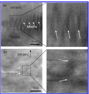
pure Ar atmosphere. The zinc oxide layer was estimated to be about 40 nm. Although the exact formula composi-tion cannot be calculated, it indicates that more oxida-tion has taken place on the surface of the polygon prismatic Zn crystals. This reveals that ZnO phase has been formed on the surface of the polygon prismatic Zn crystals and plays a role in prohibiting the sublimation of Zn. As shown in Figure 5a, the cross-sectional high-resolution TEM analysis of the polygon prismatic hollow Zn crystals demonstrates that ZnO has been formed on the surface of hollow Zn crystals. The singular fringe
spacing of the Zn was measured to be 0.24 nm, which agrees well with the (100) spacing of wurtzite-Zn, while the value of the surface ZnO is about 0.28 nm, which agrees well with the (100) spacing of wurtzite-ZnO. However, it was found that there exists a regular array of misfits (marked with arrows) at the interface between Zn and ZnO. The corresponding region of the structure fault in the Zn/ZnO core-shell is also magnified to reveal the misfits. These developed misfits possibly serve to accommodate the relatively large lattice mis-match between Zn and ZnO (17%). In contrast, as the Zn crystals were treated with prolonged oxygen anneal-ing, Figure 5b reveals that in addition to the lattice images of ZnO, many plane defects (stacking faults) as marked with arrows have developed in the ZnO layer. An enlarged representation of the marked region is also illustrated. It suggests that the hollow ZnO crystals are not perfect structures. The exact reason for this subtle change in structural morphology is not clear at this stage, but it is most likely linked to dynamic crystal growth processes at different atmospheres of Ar-O2
carrier gas. Although the synthesis of Zn single crystals was reported in the 1960s,22,23 to the authors’
knowl-edge, no hollow Zn crystals with a dimension from nanometer to micrometer were obtained at a low tem-perature based on the control between thermodynamics and kinetics.
Figure 6 illustrates the room-temperature photolu-minescence (PL) spectra of the polygon prismatic Zn crystals with or without oxidization treatment. As shown in Figure 6a, no emission peak was found for the hollow Zn crystals because the polygon prismatic Zn crystals are composed solely of pure zinc metal in this case. On the contrary, as the Zn crystals were subjected to oxidation treatment (postannealing), a thin zinc oxide layer was formed on the surface of the hollow Zn crystals according to XRD analysis. As shown in Figure 6b for the crystals annealed in air for a short time of 2 h, ultraviolet (UV) with a peak at 380 nm and green emission at∼500 nm were detected for all the Zn/ZnO crystals. The deep-level emissions (500 nm) in the hollow ZnO-Zn crystals are generally associated with defects in the ZnO lattice such as oxygen vacancies (Vo••) and zinc interstitials (Zni••) that are due to both lattice mismatch (ZnO/Zn) and incomplete oxidation of Figure 4. Depth profiles of polygon prismatic (ZnO)-Zn
crystals grown (a) in pure argon and (b) in a mixture gas of argon and oxygen at 300 °C for 2 h. The inset is the FE-SEM images of these (ZnO-)Zn crystals.
Figure 5. High-resolution TEM images of (a) hollow
hetero-structural Zn/ZnO core-shell nanocrystals and (b) ZnO nano-crystals. A magnified picture of the corresponding regions is also illustrated. The white arrowheads indicate the locations of the misfits or structure faults.
Figure 6. PL spectra recorded at room temperature with Zn
or ZnO crystals (a) grown in pure Ar, (b) annealed in air for a short period time of 2 h, and (c) postannealed in an oxygen atmosphere at 350 °C for 30 h. The PL spectra of ZnO (002) thin films are shown in the inset for comparison.
zinc. After postannealing at 300 °C for 30 h in an oxygen atmosphere, the PL of the polygon hollow ZnO-Zn crystals in Figure 6c illustrates that a stronger UV peak along with a relatively weak deep-level emission can be obtained. This further demonstrates that polygon pris-matic hollow ZnO-(Zn) crystals can be developed at a lower temperature by thermal vapor transport. How-ever, as compared with the ZnO film shown in the inset picture of Figure 6, a broader deep-level emission around∼500 nm can still be observed for all the Zn/ ZnO crystals. This indicates that more defects were generated in the polygon hollow ZnO-Zn crystals compared to ZnO film deposited on Si by radio frequency magnetron sputtering.
Conclusion
In summary, polygon prismatic hollow Zn nanocrys-tals can be grown on a Si substrate by using liquid-solution seed nucleation along with vapor-gas growth in the low-temperature range of 300-400 °C. Depending on the growth conditions (i.e., atmosphere and time), the polygon prismatic Zn nanocrystals with hollow and dense configuration can be produced as evidenced from AES analysis. Moreover, after prolonged oxidation, a zinc oxide thin layer can be developed on the surface of the hollow Zn nanocrystals to form a Zn-ZnO core-shell structure. The room-temperature PL spectra fur-ther indicate that the UV emission can be improved by controlling the oxidation to form hollow ZnO nanocrys-tals. These formed polygon hollow Zn/ZnO nanocrystals can be further used as building blocks to assemble two-or three-dimensional assemblies ftwo-or optoelectronic de-vice applications.
Acknowledgment. This work was financially sup-ported by the National Science Council of Taiwan under Contract No. NSC-92-2216-E-009-014.
References
(1) Rodriguez, J. A.; Jirsak, T.; Dvorak, J.; Sambasivan, S.; Fischer, D. J.; J. Phys. Chem. B 2000, 104, 319.
(2) Hara, K.; et al. Sol. Energy Mater. Sol. Cells 2000, 64, 115. (3) Huang, M. H.; Mao, S.; Feick, H.; Yan, H.; Wu, Y.; Kind, H.; Weber, E.; Russo, R.; Yang, P. D. Science 2001, 292, 1897.
(4) Kong, Y. C.; Yu, D. P.; Zhang, B.; Fang, W.; Feng, S. Q. Appl.
Phys. Lett. 2001, 78, 407.
(5) Park, W. I.; Jun, Y. H.; Jung, S. W.; Yi, G. C. Appl. Phys.
Lett. 2003, 82, 964.
(6) Zhang, Y.; Suenaga, K.; Collies, C.; Iijima, S. Science 1998,
281, 973.
(7) Pan, Z. W.; Dai, Z. R.; Wang, Z. L. Science 2001, 291, 1947. (8) Audebrand, N.; Auffredic, J. P.; Louer, D. Chem. Mater.
1998, 10, 2450.
(9) Huang, M. H.; Wu, Y.; Feick, H.; Tran, N.; Weber, E.; Yang, P. Adv. Mater. 2001, 13, 113.
(10) Chiou, W. T.; Wu, W. Y.; Ting, J. M. Diam. Relat. Mater.
2003, 12 (10-11), 1841.
(11) Helstand, R.; Chia, Y. Mater. Res. Soc. Symp. Proc. 1996,
73, 93.
(12) Vayssieres, L.; Keis, K.; Lindquist, S.-E.; Hagfeldt, A. J.
Phys. Chem. B, 2001, 105, 3350.
(13) Xie, Y.; Huang, J. X.; Li, B.; Liu, Y.; Qian, Y. T. Adv. Mater.
2000, 12, 1523.
(14) Braun, P. V.; Osenar, P.; Stupp, S. I. Nature 1996, 380, 325. (15) Lieber, C. M. Solid State Commun. 1998, 107, 607. (16) Alivisatos, A. P. Science 1996, 271, 933.
(17) Yamada, K.; Tobisawa, S. J. Appl. Phys. 1989, 66, 5309. (18) Driess, M.; Merz, K.; Schoenen, R.; Rabe, S.; Kruis, F. E.;
Roy, A.; Birkner, A. C. R. Chim. 2003, 6, 273.
(19) Liu, K. H.; Lin, C. C.; Chen, S. Y.; Cheng, S. Y. J.
Non-Cryst. Solids, submitted.
(20) Lin, C. C.; Liu, K. H.; Chen, S. Y.; Cheng, S. Y. J. Cryst.
Growth, in print.
(21) Li, Y.; Meng, G. W.; Zhang, L. D.; Phillipp, F. Appl. Phys.
Lett. 2000, 76, 2011.
(22) Nanev, Chr.; Iwanov, D. Phys. Status Solidi 1967, 23, 663. (23) Nanev, Chr.; Iwanov, D. J. Cryst. Growth 1968, 3/4, 530.