850 nm Zn-diffusion Vertical-Cavity Surface-Emitting Lasers with
Oxide-Relief Structure for High-Speed and Energy-Efficient Optical
Interconnects from Very-Short to Medium (2km) Reaches
Jin-Wei Shi1*, Chia-Chien Wei2, Jason (Jyehong) Chen3, and Ying-Jay Yang4 1Department of Electrical Engineering, National Central University, Taoyuan 320, Tawian
*Tel: +886-3-4227151 ext. 34466, *FAX: +886-3-4255830 *Email: [email protected]
2Department of Photonics, National Sun Yat-sen University, Kaohsiung 804, Taiwan 3Department of Photonics, National Chiao-Tung University, Hsinchu 300, Taiwan
4Department of Electrical Engineering, National Taiwan University, Taipei, 106, Taiwan
Abstract
High-speed and “green” ~850 nm vertical-cavity surface-emitting lasers (VCSELs) have lately attracted lots of attention due to their suitability for applications in optical interconnects (OIs). To further enhance the speed and its maximum allowable linking distance of VCSELs are two major trends to meet the requirement of OI in next generation data centers. Recently, by use of the advanced 850 nm VCSEL technique, data rate as high as 64 Gbit/sec over 57m and 20 Gbit/sec over 2km MMF transmission have been demonstrated, respectively. Here, we will review our recent work about 850 nm Zn-diffusion VCSELs with oxide-relief apertures to further enhance the above-mentioned performances. By using Zn-diffusion, we can not only reduce the device resistance but also manipulate the number of optical modes to benefit transmission. Combing such device, which has excellent single-mode (SMSR> 30 dB) and high-power (~7mW) performance, with advanced modulation format (OFDM), record-high bit-rate-distance-product through MMF (2.3 km×28 Gbit/sec) has been demonstrated. Furthermore, by selective etching away the oxide aperture inside Zn-diffusion VCSEL, significant enhancement of device speed, D-factor, and reliability can be observed. With such unique VCSEL structure, >40 Gbit/sec energy-efficient transmission over 100m MMF under extremely low-driving current density (< 10kA/cm2) has been successfully demonstrated. Key words: Green Photonics, Vertical-Cavity Surface-Emitting Lasers, Optical Interconnect
1. INTRODUCTION
The continuous growth in global Internet Protocol traffic, fueled by on-demand Internet streaming media, remote office services, and electronic commerce, doubles almost every two years. In order to handle the enormous cloud computation and storage, modern data centers urgently require that interconnects can be operated at a high bit rate (of at least 25 Gbps before 2020 [1]) over links of few kilometers [2]. Optical interconnects (OIs) have been widely studied and envisioned as a promising candidate for short-distance communication. High-speed, high-efficiency, and low power consumption vertical-cavity surface-emitting lasers (VCSELs) that operate at a wavelength of 850nm or around 1000 nm have lately attracted a lot of attention due to their suitability for applications in OIs [3-11]. To further enhance the modulation speed of VCSELs is one of the most important ways to increase the data rate of next generation OIs. Using multiple oxide layers with oxide aperture diameter less than 5 µm is usually necessary to reduce the parasitic capacitance and enhance speed performance of VCSEL structures [3,5-7]. Through the use of these VCSELs, energy efficient >40 Gbit/sec transmission of 850 nm VCSEL has been demonstrated [6,7] for very-short reach (VSR) linking distance (~50 meter). However, the small current-confined aperture (< 4 µm) in these devices would usually result in large differential resistance (> 120 Ω) and impedance mismatch between VCSELs and driver ICs, which may degrade eye-patterns due to microwave reflections [5]. Furthermore, the high operation current density (~43.3 kA/cm2 [3]; ~25 kA/cm2 [4,6,7]) and the significant stress between multiple oxide layers and surrounding semiconductor active layers are both issues for the reliability performances.
The other important issue in the development of VCSEL is to narrow down its spectral width and improve the maximum allowable bit-rate distance product [6,9,12]. The reported high-speed 850 nm VCSELs are usually multimode. Their transmission performance are thus usually limited from the modal and chromatic dispersion in the multimode fiber (MMF), notably the transmission at higher bit rate (>40 Gbps) suffers larger dispersion, leading to that the transmitted data rate drops substantially as the fiber length increases. In general, there are two main approaches to further extend the bit-rate distance product of MMF. One is using quasi single-mode or single-mode VCSELs. By the use of (quasi-) single-mode VCSELs with narrow spectral-width performances, excellent transmission performance through >1km MMF with on-off keying (OOK) modulation format at 850 nm wavelength have been demonstrated [6,9,12]. Another approach is using the integrated circuit (IC) -based signal equalization and compensation. By the use of a 2-tap pre-emphasis driver IC, a 40 Gbps VCSEL operation was demonstrated [13]. Moreover, a 64 Gbps 850nm VCSEL operation over 57 m using two tap feed forward equalization was experimentally demonstrated [3], opening up the possibility of a higher bit rate by employing IC-based signal equalization. Furthermore, with the remarkable advances in ICs, the rapid development of digital-signal-processing (DSP) technology and catalysis of the 100 Gbps coherent optical transmission system, high-speed analog-to-digital
Invited Paper
Vertical-Cavity Surface-Emitting Lasers XIX, edited by Chun Lei, Kent D. Choquette, Proc. of SPIE Vol. 9381, 93810E · © 2015 SPIE · CCC code: 0277-786X/15/$18 · doi: 10.1117/12.2085061
Wz P contact k- Zn diffusion Oxide relief Active region N contact Si02 0.5 7L Cavity, AIInGaAs /AIGaAs MQW (b) Pad
ti
PMGI 1.5 7L Cavity, SiO2 GaAs /AIGaAs MQW W= P contact Zn diffusion Oxide relief Active region N contact n + GaAs substrateconverters (ADCs) and digital-to-analog converters (DACs) have gradually matured with increased availability and lower power consumption [14, 15]. Such the momentum facilitates orthogonal frequency-division multiplexing (OFDM) format to be increasingly regarded as an alternative means for achieving the higher bit-rate distance product (BRDP) of data communication [16, 17].
Here, we will review our recent work about 850 nm Zn-diffusion VCSELs with oxide-relief apertures to further enhance the above-mentioned performances. By using Zn-diffusion, we can not only reduce the device resistance but also manipulate the number of optical modes to benefit transmission. Combing such device, which has excellent single-mode (SMSR> 30 dB) and high-power (~7mW) performance, with advanced modulation format (OFDM), record-high bit-rate-distance-product through MMF (2.3 km× 28 Gbit/sec) has been demonstrated [17]. Furthermore, by selective etching away the oxide aperture inside Zn-diffusion VCSEL, significant enhancement of device speed, D-factor, and reliability can be observed. With such unique VCSEL structure, >40 Gbit/sec energy-efficient transmission over 100m MMF under extremely low-driving current density (< 10kA/cm2) has been successfully demonstrated [18].
2. DEVICE STRUCTURE
Figures 1 (a) and (b) show the conceptual cross-sectional views of two kinds of devices for high-speed and single-mode/high-power operations, respectively. Both devices have the same top views, as shown in Figure 1 (c).
As shown in Figure 1 (a), the epi-layer structure for high-speed VCSEL is grown on a semi-insulating (S.I.) GaAs substrate, which is composed of three In0.15Al0.1Ga0.75As/Al0.3Ga0.7As MQWs sandwiched between a 30-pair n-type and a 20-pair p-type Al0.9Ga0.1As/ Al0.12Ga0.88As Distributed-Bragg-Reflector (DBR) layers with an Al0.98Ga0.02As layer above the MQWs for oxidation. Here, the cavity layer thickness is shortened to λ/2 in order to shorten the internal carrier transient time and increase the optical confinement factor [4,6]. Compared with that reported for In0.1Ga0.9As/Al0.37Ga0.63As strained 850nm VCSELs [19], we can achieve a higher indium mole fraction (0.15 vs. 0.1) with a thicker well-width (50 vs. 40Å) due to the incorporation of Al, which enlarges the bandgap but has no significant influence on the lattice constant (strain) of the well layer. This means our strained VCSEL structure has a higher indium mole fraction and a wider well-width than those of InGaAs based strained 850nm VCSELs [19] which may lead to a more significant improvement in static/dynamic performance and uniformity of wafer, respectively.
As shown in Figure 1 (b), there are three major differences in the epi-layer structure between high-power single-mode VCSEL and high-speed VCSEL. First is that the epi-layer structure was grown on the n+ GaAs substrate instead of on S.I. substrate. This is because that n+ substrate can provide better heat-sinking for high-power operation than that of S.I. substrate. In addition, the parasitic RC-limited bandwidth, which can be mitigated by use of S.I. substrate, is not a major E-O bandwidth limiting factor for the case of high-power single-mode VCSELs. Their speed performance is usually limited by spatial hole burning effect [9]. Second is that we enlarge the cavity layer thickness to 3λ/2 to dilute the optical confinement and increase the maximum saturation power. Third is that for high-power structure, we use GaAs/Al0.3Ga0.7As MQWs active layer due to its larger density state as compared to that of In0.15Al0.1Ga0.75As well, which might benefit for high power operation.
Figure 1. Conceptual cross-sectional views of (a) high-speed VCSEL on S.I. substrate and (b) single-mode/high-power VCSEL on n+ GaAs substrate. (c) shows the top-view of fabricated devices
A: Oxide Relief B: Non -Relief 3mA m. ®5IN = 7.58
s
SIN = 5.02 5mA m. SIN = 7.74 SIN = 5.37 7mA SIN = 8.32 m SIN = 5.78 A single-oxide layer and oxidation technique is used to define a circular current-confined area for both structures. By use of the chemical solution, which offers excellent etching selectivity between the AlxO1-x layer and active (Al(In)GaAs) layers, we can remove this layer without degrading the device performances [8,9]. Due to the fact that the dielectric constant of air is just around one-half that of the AlxO1-x layer, there is a further reduction in the parasitic capacitance, as confirmed by microwave scattering (S) parameter measurement and device modeling techniques carried out on the oxide-relief and control VCSELs [8]. During device fabrication, we can control three most important parameters, d, Wo, Wz, as specified on Figure 1 (a) and (b), to manipulate the device static/dynamic performance [8,9]. Where, Wo is the oxide-relief diameter, d is the Zn-diffusion depth, and Wz is the diameter of Zn-diffusion aperture. For the case of single-mode device, a larger size of Wo than that of Wz is necessary to have significant intra-cavity loss and result in stable single-mode performance. As can be seen in Figure 1 (c), the fabricated device has a 26 µm diameter active mesa, which is integrated with co-planar waveguide (CPW) pads for on-wafer high-speed measurement.3.
MEASUREMENT RESULTS
3.1 Oxide vs. Oxide-Relief VCSLEs
As discussed previously, the oxide-relief process can reduce the parasitic capacitance of VCSELs and further enhance their speed performance. However, the relief process results in a more significant index contrast in the current-confined regime. This might induce more optical transverse modes in the cavity and make the single-mode performance become more difficult. In order to investigate this effect, two kinds of device structure with (A) and without (B) oxide-relief processes were fabricated by use of high-power epi-layer structure as shown in Figure 1 (b). These two devices have the same WZ, WO, and d of 5, 5.5, and 1.0 µm, respectively. Figure 2 shows the measured power (voltage) versus current (L-I and V-I) curves of devices A (A1 and A2) and B (B1 and B2).
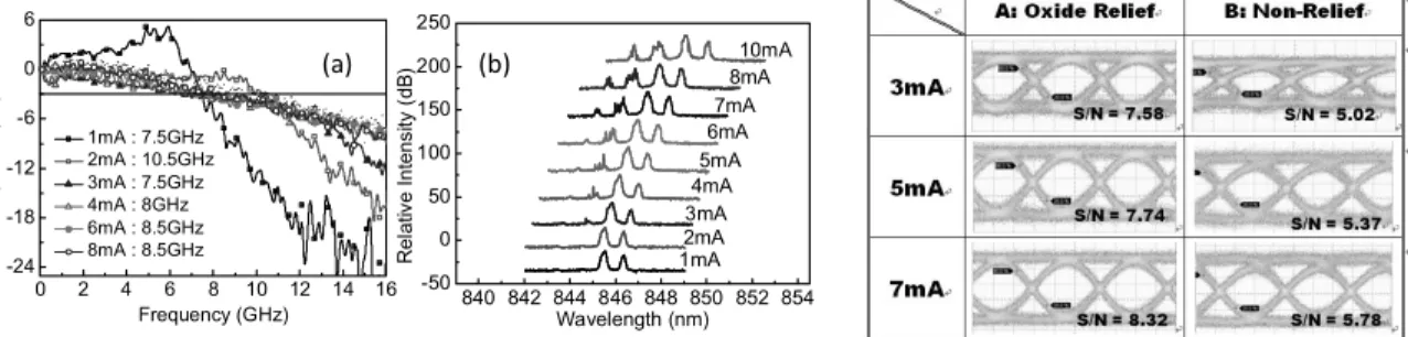
As can be seen, the relief structure (device A) usually has slightly better L-I and V-I performances than the non-relief structure (device B). Such result might be attributable to the oxide-relief process which can partially eliminate the defect states which exist at the interface between the current-confined oxide layers and semiconductor epitaxial layers. Slight improvements in the V-I performance, current injection efficiency into the active layers, differential quantum efficiency, and output optical power can thus be observed in device A with the oxide-relief structure. Figures 3 and 4 shows the measured electrical-to-optical (E-O) frequency responses and optical spectra for devices A and B, respectively. We can clearly see that the optical mode spectra under different bias currents are very similar for both devices, and due to the implementation of the Zn-diffusion process for optical mode control, both devices exhibit quasi single-mode behavior under the low bias current (< 3 mA) regime. Furthermore, compared with device B, device A has a larger maximum 3-dB E-O bandwidth (13 vs. 10.5 GHz) due to the reduction in parasitic capacitance [16].
0 2 4 6 8 10 12 14 16 0 2 4 6 8 P o w e r (m W ) Current (mA) Relief A1 Relief A2 Non-Relief B1 Non-Relief B2 0 1 2 3 4 5 Volt age (V )
Device A1, A2 =76 Ω at 6mA Device B1=78 Ω at 6mA Device B2=106 Ω at 6mA 0 2 4 6 8 10 12 14 16 -24 -18 -12 -6 0 6 R es pons e ( dB ) Frequency (GHz) 1mA : 8.5GHz 2mA : 11GHz 3mA : 12GHz 4mA : 13GHz 6mA : 11GHz 8mA : 10GHz (a) (b) 840 842 844 846 848 850 852 854 -50 0 50 100 150 200 250 10mA 8mA 7mA 6mA 5mA 4mA 2mA 3mA R el ati ve Intens ity ( dB ) Wavelength (nm) 1mA 0 2 4 6 8 10 12 14 16 -24 -18 -12 -6 0 6 Res pons e ( dB ) Frequency (GHz) 1mA : 7.5GHz 2mA : 10.5GHz 3mA : 7.5GHz 4mA : 8GHz 6mA : 8.5GHz 8mA : 8.5GHz (a) (b) 840 842 844 846 848 850 852 854 -50 0 50 100 150 200 250 10mA 8mA 7mA 6mA 5mA 4mA 3mA 2mA R el ati ve Intens ity ( dB ) Wavelength (nm) 1mA Figure 2. Characteristics of the optical output power (L) and voltage (V) versus biasing current (I) of devices A (Wz/Wo/d=5/5.5/1 µm) and B (Wz/Wo/d=5/5.5/1 µm).
Figure 3. Measured E-O frequency responses (a) and output optical spectra (b) of device A (Wz/Wo/d=5/5.5/1 µm) under
different bias currents
Figure 4. Measured E-O frequency responses (a) and output optical spectra (b) of device B (Wz/Wo/d=5/5.5/1 µm) under
different bias currents
Figure 5. Measured back-to-back eye-patterns of devices A (Wz/Wo/d=5/5.5/1 µm) and B (Wz/Wo/d=5/5.5/1 µm) under 15
9 83 10 LY `1 m 77 1-31 73 O 77 ' 12 13 3 4 5 6 Current (mA) 7 These dynamic and static measurement results clearly indicate that our oxide-relief process will not degrade the dc characteristics, which include L-I, V-I, and the output optical spectra of VCSELs and can significantly further improve the speed performance of the device. Figure 5 shows the measured back-to-back and error-free eye-patterns of devices A and B under different bias currents at the same data rate as 15 Gbit/sec. We can clearly see that the measured eye-patterns of device A have a shorter rise/fall time and a higher signal-to-noise (S/N) ratio than those of device B. The superior eye-pattern performance of device A compared to device B can be attributed to the better speed performance of device A as discussed in Figures 3 and 4.
3.2 High-Speed (> 41 Gbit/sec) VCSELs
As shown in Figure 1 (a), by combing the short cavity length (λ/2), oxide-relief and Zn-diffusion apertures, a very-high speed 850 nm VCSEL has been demonstrated [18]. Figure 6 (a) shows the light output versus current (L-I) and the bias current versus voltage (I-V) characteristics of the demonstrated oxide-relief/Zn-diffusion VCSEL at RT and 85℃. Its conceptual cross-sectional view is given in Figure 1 (a). As can be seen, our device exhibits a reasonable threshold current (~0.4 mA) and there is no significant increase in threshold current even when the ambient temperature is raised up to 85℃. Such excellent high-temperature performance can be attributed to large detuning (~20 nm) between gain peak of MQWs (~838 nm) and Fabry-Perot dip (~858 nm). Furthermore, thanks to the large diameter of oxide current-confined aperture (~7.5 µm), the measured differential resistance of our device can be as low as ~60 Ω under the small operation current ~4 mA. Such a value is much smaller than the values typically reported for high-speed VCSELs for 40 Gbit/sec operations (~ 100 Ω) [3-7]. Figure 6 (b) shows the measured optical spectra under different bias currents at RT operation. As can be seen, thanks to the Zn-diffusion aperture in our VCSEL for optical mode control [8,9], our device can exhibit quasi-single mode performance under low bias current (< 4 mA) even with a large diameter of oxide aperture (~7.5 µm), which would benefit the transmission performance as discussed latter.
Figure 7 shows the measured E-O responses of device under different bias currents. As can be seen, our device can achieve 26 GHz 3-dB bandwidth with bias current as low as 8 mA. Such value is less than the required bias current (8 vs. 12.1 mA) of the reported 40 Gbit/sec 850 nm VCSEL with a close size of oxide diameter (~7 µm) and E-O bandwidth performance (~27 GHz) [4]. Figure 8 (a) shows the measured 41 Gbit/sec eye-patterns of our device for the case of back-to-back (BTB) and over 100 meter OM4 fiber. In our setup for data transmission, the receiver-end is composed of a commercialized photoreceiver (VI-Systems R40–850 photoreceiver), which has a 30 GHz 3-dB O-E bandwidth and good performance for >40 Gbit/sec eye-detection [4,6,7]. The length and amplitude (Vpp) of electrical pseudorandom binary sequence (PRBS) patterns used for our transmission experiment is fixed at 215-1 and 0.5 V, respectively. We can clearly see that when the bias current is over 3 mA, clear 41 Gbit/sec eye-opening can be achieved for both cases. Figure 8 (b) shows the measured –log (bit-error-rate (BER)) values versus bias current of our device at 41 Gbit/sec operations. The corresponding error-free eye-patterns are also specified. Under RT operation, the energy-to-data rate (EDR) for 100 meter OM4 fiber transmission is as low as 228 fJ/bit (3.5 mA).
852 854 856 858 860 862 864 866 Re la tiv e in te ns ity (d B ) Wavelength(nm) 2mA 4mA 6mA 8mA 0 1 2 3 4 5 6 7 8 9 0.0 0.2 0.4 0.6 0.8 1.0 1.2 1.4 Pow er ( m W ) Current (mA) RT 85 degree C 0 1 2 3 4 5 Volt age ( V ) (a) (b)
Figure 6. (a) Measured L-I and I-V curves and (b) measured optical spectra of demonstrated device under different bias currents (Wz/Wo/d=7.5/7.5/1 µm). 0 5 10 15 20 25 30 -30 -24 -18 -12 -6 0 6 R e spons e (dB ) Frequency(GHz) 2mA(12GHz) 4mA(22GHz) 6mA(23GHz) 8mA(26GHz)
Figure 7. Measured E-O frequency responses at different bias currents (Wz/Wo/d=7.5/7.5/1 µm) .
Figure 8 (a) Measured 41 Gbit/sec eye-patterns under different bias currents for BTB and 100 m OM4 fiber transmission. (b) Measured –log (BER) values under different bias currents for 100 m OM4 fiber transmission (Wz/Wo/d=7.5/7.5/1 µm).
(a)
Such number is close to the reported lowest EDR value for 40 Gbit/sec transmission of 850 nm VCSEL (158 [6] vs. 228 fJ/bit), which is measured under the case of a much shorter linking distance (50 vs. 100 meter MMF) than that of ours. Furthermore, thanks to the advanced active layer design with highly strained MQWs in our VCSEL structure, a record low driving-current density (~8 kA/cm2; 3.5 mA) for error-free operation with a longer linking distance (100 vs. 50 meters MMF) as compared to those of reported state-of-the-art 850 nm VCSELs [3-8], which usually have driving density > 25 kA/cm2 for >40 Gbit/sec transmission [3-8], has been successfully demonstrated [18].
3.3 Single-Mode and High-Power VCSELs
In order to further extend the maximum transmission distance in OM4 fiber, a further optimization in the geometric sizes (Wz, Wo, and d) of our VCSEL to let it have single-mode and high-power performance is highly desired. The key to achieve single-mode performance is to suppress the optical transverse modes inside the gain region (current-confined region) of VCSEL cavity by use of Zn-diffusion aperture, which can not only reduce the reflectivity of DBR layers but also increase the free carrier absorption loss in the Zn-diffused area. Based on these points, we can expect that in order to have single-mode performance, we must let WO > WZ, which results in the significant Zn-diffusion induced loss in the current-confined regime. In addition, the size of WZ is also a criterion for the single-mode performance. According to our previous work [9], the size of optical confined aperture (WZ) in our adopted epi-layer structure, as shown in Figure 1 (b), must be smaller than 6.5 µm to ensure single-mode (SM) operation at 850 nm. Figure 9 and 10 shows the measured L-I/V-I characteristics and optical spectra under different bias currents of single-mode VCESLs, respectively. Their geometric sizes (WO, WZ, and d) are specified in these two figures. As can be seen, our device can sustain single-mode performance with a ~30 dB side-mode suppression ratio (SMSR) under the full range of bias current and have a reasonable threshold current at around 1.5 to 2.5 mA. The spectral width is measured by Advantest Q8384 optical spectrum analyzer with a smallest resolution of 0.01 nm. The measurement results for our single mode VSCEL is as narrow as around 0.08 nm (18.2 GHz spectral width), which is insensitive to the variation in bias currents. Fig. 11 shows the measured typical E-O frequency responses of our single-mode VCSEL. A reasonable high-speed performance (~11 GHz) with minimized low-frequency roll-off can be achieved in this device due to the optimization of our cavity size [9]. As above discussion, the simple OOK modulation scheme and multi-mode characteristics of our high-speed VCSELs would suffer from serious chromatic dispersion, which would seriously limit its maximum bit-rate distance product (BRDP) for transmission. To use advanced modulation format onto single-mode VCSEL is one possible solution to overcome such problem. Fig. 12 shows the experimental setup of our demonstrated SM VCSEL for OFDM transmission. The electrical OFDM signal is carried out by an arbitrary waveform generator (AWG, Tektronix® AWG7122) at the sampling rate of 10 GSample/s, and the digital-to-analog (D/A) conversion resolution is of 8 bit and the output peak-to-peak voltage is of 1 V. Our OFDM coding is realized by using offline technique (Matlab®) with fast Fourier transform (FFT) size of 512, cyclic prefix (CP) of 3.03%, and 4.9 GHz bandwidth. Fig. 13 (a) shows the signal-to-noise ratios (SNRs) of OFDM signals at electrical back to back (EBTB) and after 2.3-km OM4 MMF transmission with the bias current of 9 mA, respectively. Fig. 13 (b) shows the SNRs of OFDM signals after 2.3-km MMF transmission with bit-loading algorithm to utilize the bandwidth more effectively. Fig. 13 (c) shows the corresponding modulation levels of the OFDM subcarriers after 2.3-km MMF transmission, and the total bit rate is up to 28.03 Gbps, and Fig. 13 (d) shows the constellations of the OFDM signal. According to the measured BER of 1.4×10⁻³, the 28-Gbps OFDM signal can achieve the FEC limit of 3.8×10⁻³ after 2.3-km OM4 MMF transmission. This is corresponding to a record-high BRDP of 64.4 Gbps·km [17].
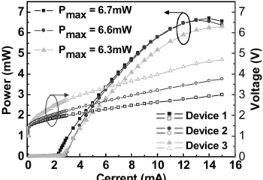
0 2 4 6 8 10 12 14 16 0 1 2 3 4 5 6 7 Pmax = 6.7mW Pmax = 6.6mW Pmax = 6.3mW V o lt ag e ( V ) Pow e r (m W ) Cerrent (mA) Device 1 Device 2 Device 3 0 1 2 3 4 5 6 7 846 848 850 852 854 -150 -100 -50 0 50 SMSR = 31.5 dB SMSR = 37.2 dB SMSR = 36.8 dB SMSR = 36.6 dB R elat ive in te n sity (d B ) Wavelength (nm) 12mA 9mA 6mA 3mA
Figure 9. LIV characteristics of three single-mode VCSELs (Wz/Wo/d=6/8.5/2 µm)
Figure 10. Measured optical spectra and SMSR under different bias currents of single-mode VCSELs (Wz/Wo/d=6/8.5/2 µm)
0 2 4 6 8 10 12 14 16 18 20 -40 -30 -20 -10 0 10 R esponse ( d B ) Frequency (GHz) 3mA : 5 GHz 12mA : 12 GHz 0 1 2 3 4 5 10 15 20 25 30 Received power = -3dBm S N R (d B) Frequency (GHz) EBTB 2.3 km Bias current = 9 mA (a) 0 1 2 3 4 5 10 15 20 25 30 Bias current = 9 mA (b) S N R (d B) Frequency (GHz) 2.3 km Received power = -3dBm 0 1 2 3 4 5 4 5 6 7 8 Bit rate = 28.03 Gbps (c) Modul at ion l ev e l ( b it ) Frequency (GHz)
4. CONCLUSIONS
By using Zn-diffusion and oxide-relief structures, two kinds of high-performance 850 nm VCSELs for
short-reach (SR; <300 meter) and medium-reach (MR: <2 km) transmission with high data-rate have been demonstrated. For the case of SR applications, our oxide-relief and Zn-diffusion structures can effectively reduce the parasitic capacitance and differential resistance, respectively. The RC-limited bandwidth and current modulation efficiency (D-factor) can thus be further improved. Record-low driving current density (~8 kA/cm2) for > 40 Gbit/sec transmission over 100 meter OM4 fiber has been demonstrated. On the other hand, by controlling the relative sizes of Zn-diffusion and oxide-relief apertures (Wz/Wo), high single-mode output power (~7 mW, SMSR> 30 dB) with moderate high-speed (~11 GHz) performance of 850 nm VCSEL has been demonstrated. By combing such device with advanced OFDM modulation format, record-high BRDP (64.4 Gbps.km) through 2.3 km OM4 fiber and at 850 nm wavelength has been successfully demonstrated.
Figure 11. Measured E-O frequency responses of the demonstrated single-mode VCSEL under different bias currents (Wz/Wo/d=6/8.5/2 µm).
Figure 12. OFDM experimental setup
Figure 13. (a) SNRs of EBTB and after 2.3-km MMF. (b) SNRs after 2.3-km MMF with bit-loading algorithm at bias current of 9 mA. (c) Modulation levels of the OFDM subcarriers. (d) Constellations after transmission.
Technology, vol. 30, No. 4, pp. 448-458, Feb., 2012.
[2] C. F. Lam, H. Liu, B. Koley, X. Zhao, V. Kamalov, and V. Gill, “Fiber Optic Communication Technologies: What’s Needed for Datacenter Network Operations,” IEEE Communication Magazine, vol. 48, no. 7, pp. 32-39, 2010.
[3] D. M. Kuchta, A. V. Rylyakov, C. L. Schow, J. E. Proesel, C. Baks, P. Westbergh, J. S. Gustavsson, and A. Larsson, “64Gb/s Transmission over 57m MMF using an NRZ Modulated 850nm VCSEL,” Proc. OFC 2014,
San Francisco, CA, USA, March, 2014, pp. Th3C. 2.
[4] P. Westbergh, R. Safaisini, E. Haglund, J. S. Gustavsson, A. Larsson, M. Geen, R. Lawrence, and A, Joel, “High-Speed Oxide Confined 850-nm VCSELs Operating Error-Free at 40 Gb/s up to 85℃,” IEEE Photon.
Technol. Lett., vol. 25, pp.768-771, April, 2013.
[5] P. Westbergh, R. Safaisini, E. Haglund, B. Kogel, J. S. Gustavsson, A. Larsson, M. Geen, R. Lawrence, and A, Joel, “High-Speed 850 nm VCSELs with 28 GHz modulation bandwidth operating error-free up to 44 Gbit/s,”
Electron. Lett., vol. 48, no. 18, Aug., 2012.
[6] P. Moser, P. Wolf, G. Larisch, H. Li, J. A. Lott, and D. Bimberg, “Energy-efficient oxide-confined high-speed VCSELs for optical interconnects,” Proc. SPIE, Vertical-Cavity Surface Emitting Lasers XVIII, vol. 9001, pp. 900103, Feb., 2014.
[7] P. Wolf, P. Moser, G. Larisch, H. Li, J. A. Lott, and D. Bimberg, “Energy efficient 40 Gbit/s transmission with 850 nm VCSELs at 108 fJ/bit dissipated heat,” Electron. Lett., vol. 49, no. 10, May, 2013.
[8] Jin-Wei Shi, Jhih-Cheng Yan, Jhih-Min Wun, Jason (Jyehong) Chen, Ying-Jay Yang, “Oxide-Relief and Zn-Diffusion 850 nm Vertical-Cavity Surface-Emitting Lasers with Extremely Low Energy-to-Data-Rate Ratios for 40 Gbit/sec Operations” IEEE J. of Sel. Topics in Quantum Electronics, vol. 19, pp. 7900208, March/April, 2013.
[9] Jin-Wei Shi, Zhi-Rui Wei, Kai-Lun Chi, Jia-Wei Jiang, Jhih-Min Wun, I-Cheng Lu, Jason (Jyehong) Chen, and Ying-Jay Yang, “Single-Mode, High-Speed, and High-Power Vertical-Cavity Surface-Emitting Lasers at 850 nm for Short to Medium Reach (2 km) Optical Interconnects,” IEEE/OSA Journal of Lightwave Technology, vol. 31, pp. 4037-4044, Dec., 2013.
[10] S. Imai, K. Takaki, S. Kamiya, H. Shimizu, J. Yoshida, Y. Kawakita, T. Takagi, K. Hiraiwa, H. Shimizu, T. Suzuki, N. Iwai, T. Ishikawa, N. Tsukiji, and A. Kasukawa, “Recorded Low Power Dissipation in Highly Reliable 1060-nm VCSELs for “Green” Optical Interconnection,” IEEE J. Sel. Topics Quantum Electron., vol. 17, no. 6, pp. 1614–1619, Nov./Dec. 2011.
[11] P. Moser, P. Wolf, A. Mutig, G. Larisch, W. Unrau, W. Hofmann, and D. Bimberg, “85 ℃ error-free operation at 38 Gb/s of oxide-confined 980-nm vertical-cavity surface-emitting lasers,” Appl. Phys. Lett., vol. 100, no. 8, pp. 081103, Feb., 2012.
[12] R. Safaisini, E. Haglund, P. Westbergh, J.S. Gustavsson, and A. Larsson, “20 Gbit/s data transmission over 2 km multimode fibre using 850 nm mode filter VCSEL,”Electron. Lett., vol. 50, no. 1, pp. 40-42, Jan., 2014.
[13] Y. Tsunoda, M. Sugawara, H. Oku, S. Ide, and K. Tanaka, “A 40-Gb/s VCSEL Transmitter for Optical Interconnect with Group-Delay Compensation Pre-Emphasis,” Proc. OFC 2014, San Francisco, CA, USA, March, 2014, pp. Th3C. 3.
[14]R. Bouziane, P. Milder, R. Koutsoyannis, Y. Benlachtar, J. C. Hoe, M. Püschel, M. Glick, and R. I. Killey, "Design studies for ASIC implementations of 28 GS/s optical QPSK- and 16-QAM-OFDM transceivers," Opt.
Exp., vol. 19, pp. 20857–20864, 10/10 2011.
[15] P. A. Milder, R. Bouziane, R. Koutsoyannis, C. R. Berger, Y. Benlachtar, R. I. Killey, M. Glick, and J. C. Hoe, "Design and simulation of 25 Gb/s optical OFDM transceiver ASICs," Opt. Exp., vol. 19, pp. B337–B342, 12/12 2011.
[16] S.C.J. Lee, F. Breyer, S. Randel, D. Cárdenas, H.P.A. van den Boom, and A.M.J. Koonen, “Discrete Multitone Modulation for High-Speed Data Transmission over Multimode Fibers using 850-nm VCSEL,” Proc. OFC
2009, San Diego, CA, USA, March, 2009, pp. OWM2.
REFERENCES
[17] I-Cheng Lu, Chia-Chien Wei, Jin-Wei Shi, Hsing-Yu Chen, Sheng-Fan Tsai, Zhi-Rui Wei, Jhih-Min Wun, Jun-Xing Wu, and Jyehong Chen, “A 64.4 Gbps·km Optical Interconnect Employing a High-Power High-Speed Single-Mode 850-nm VCSELs and OFDM Format,” ECOC 2013, London, UK, Sep., pp. Th.2.F.2.
[18]Kai-Lun Chi, Jia-Wei Jiang, Jia-Liang Yen,I-Cheng Lu, H.-C. Kuo, Jason (Jyehong) Chen, Ying-Jay Yang, Chia-Chien Wei, and Jin-Wei Shi, “Energy Efficient 850 nm Vertical-Cavity Surface-Emitting Lasers with Extremely Low Driving-Current Density for >40 Gbit/sec Error-Free Transmissions from RT to 85℃,”to be published in OFC 2015, Los Angeles, CA, USA, March, 2015, pp. M2D.6
[19] S. B. Healy, E. P. O’Reilly, J. S. Gustavsson, P. Westbergh, and A. Haglund, A. Larsson, and A. Joel, “Active Region Design for High-Speed 850-nm VCSELs,” IEEE J. Quantum Electron., vol. 46, pp. 506-512, April, 2010.