Massive spalling of intermetallic compounds in solder-substrate reactions
due to limited supply of the active element
S. C. Yang, C. E. Ho, and C. W. Chang
Department of Chemical & Materials Engineering, National Central University, Jhongli City, Taiwan C. R. Kaoa兲
Department of Materials Science and Engineering, National Taiwan University, Taipei, Taiwan 共Received 4 January 2007; accepted 9 February 2007; published online 23 April 2007兲
Massive spalling of intermetallic compounds has been reported in the literature for several solder/ substrate systems, including SnAgCu soldered on Ni substrate, SnZn on Cu, high-Pb PbSn on Cu, and high-Pb PbSn on Ni. In this work, a unified thermodynamic argument is proposed to explain this rather unusual phenomenon. According to this argument, two necessary conditions must be met. The number one condition is that at least one of the reactive constituents of the solder must be present in a limited amount, and the second condition is that the soldering reaction has to be very sensitive to its concentration. With the growth of intermetallic, more and more atoms of this constituent are extracted out of the solder and incorporated into the intermetallic. As the concentration of this constituent decreases, the original intermetallic at the interface becomes a nonequilibrium phase, and the spalling of the original intermetallic occurs. © 2007 American Institute of Physics. 关DOI:10.1063/1.2717564兴
I. INTRODUCTION
Solder joints play at least two important roles in elec-tronic packages: they serve as electrical interconnections be-tween components and as mechanical support for the de-vices. Unfortunately, solder joints have long been recognized as the weak links of an electronic package, and the reliability of each individual joint determines the overall lifespan of an electronic product. One important factor influencing the sol-der joint reliability is the interfacial reaction between the solder and the substrate during soldering and the subsequent aging. Consequently, knowledge of solder/substrate reactions is necessary in order to improve the reliability of electronic products.
One interesting issue in solder/substrate reactions is the spalling of intermetallic compounds from the solder/ substrate interface. Here, spalling refers to the detachment of the intermetallic compound, the reaction product, from the interface during the reaction. A classical example is the spal-ling of Cu6Sn5during the reaction between the PbSn solder
and the Cu/Cu-Cr thin-film metallization.1,2 Spalling here was caused by the exhaustion of the Cu film, which had a good wetting with Cu6Sn5, and the subsequent direct contact
between Cu6Sn5and the remaining Cu-Cr layer, which had a
relatively poor wetting with Cu6Sn5. This poor wetting
be-tween Cu-Cr and Cu6Sn5 caused the molten solder to
pen-etrate into the roots of the Cu6Sn5 grains, leading to the
spalling of Cu6Sn5grains into the molten solder.
Recently, another type of spalling was observed in sev-eral solder/substrate systems, including SnAgCu soldered on Ni substrate,3–5 SnZn on Cu,6 high-Pb PbSn on Cu,7,8 and high-Pb PbSn on Ni.9 In these solder/substrate systems, the intermetallics detached themselves in a massive scale during
reflow, even though the wetting layer had not been depleted. Such a phenomenon was referred to as massive spalling.3,4In short, the massive spalling differs from the regular spalling in two ways: the apparent difference in the scale of spalling and the fact that massive spalling can occur even when the wettable layer is intact. Despite the fact that massive spalling has been observed across several solder/substrate systems, a unified explanation to rationalize this behavior is still lack-ing. The major objective of this article is to propose a thermodynamic argument to explain this rather peculiar phenomenon.
II. MASSIVE SPALLING DUE TO THE SHIFTING OF THE EQUILIBRIUM PHASE
In the following, the proposed argument and the support-ing thermodynamic evidence for the massive spallsupport-ing in SnAgCu/Ni will be presented in detail. The same argument will then be applied to the other three systems: SnZn/Cu, high-Pb PbSn/Cu, and high-Pb PbSn/Ni.
A. Massive spalling in SnAgCu/Ni
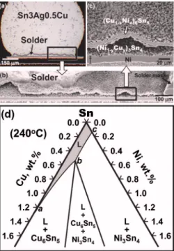
A typical example of the massive spalling is shown in Figs. 1共a兲–1共c兲 for a 760m diam Sn3Ag0.5Cu 共wt. %, same below兲 solder ball soldered over a Au/Ni substrate with a 600m diam opening. During reflow, the peak reflow tem-perature was 235 ° C and the time during which the solder was molten was 5 min. The outer 共Cu1−xNix兲6Sn5 layer had
detached itself from the interface. The intermetallic com-pound that was still attached to the Ni layer was 共Ni1−yCuy兲3Sn4. The gap between these two layers was
origi-nally occupied by the solder, but the solder there was etched away during sample preparation. It is clear from Figs. 1共a兲 a兲Electronic mail: [email protected]
and 1共c兲 that the spalling occurred across the entire joint. More intriguing micrographs showing the massive spalling can be found in the articles by Ho et al.3,4
To understand the occurrence of massive spalling even in the presence of an intact wettable Ni layer, one has to start from the phase equilibrium of the relevant elements. The Sn-rich corner of the Sn-Cu-Ni isotherm at 240 ° C is shown in Fig.1共d兲.4The constituent Ag is inert as far as the inter-facial reaction is concerned and can be ignored in the present analysis.10,11This isotherm shows that solders with different Cu concentration are in equilibrium with different phases. When the Cu concentration is high 共between a and b兲, the molten solder is in equilibrium with 共Cu1−xNix兲6Sn5, and
when the Cu concentration is low 共between b and c兲, the molten solder is in equilibrium with共Ni1−yCuy兲3Sn4. At point b, the molten solder,共Ni1−yCuy兲3Sn4, and共Ni1−yCuy兲3Sn4are
in three-phase equilibrium. According to this isotherm, one might anticipate that the reaction between Ni and the molten solder with different Cu concentrations would produce dif-ferent compounds at the interface. This strong Cu concentra-tion dependency indeed had been observed experimentally in the reaction between SnCu solder and Ni,12 as well as be-tween SnAgCu and Ni.10,11 It was found that, upon increas-ing the Cu concentration, the reaction product changed from single-phase 共Ni1−yCuy兲3Sn4, to two-phase 共Ni1−yCuy兲3Sn4
+共Cu1−xNix兲6Sn5, and then to single-phase
共Cu1−xNix兲6Sn5.10–12 As 共Cu1−xNix兲6Sn5 or 共Ni1−yCuy兲3Sn4
grew thicker, more and more Cu atoms in the solder were extracted out of the solder and became incorporated into
共Cu1−xNix兲6Sn5, or 共Ni1−yCuy兲3Sn4. Consequently, if the Cu
concentration of the solder is not maintained at a constant level by certain means, the Cu concentration of solder will decrease with the growth of the reaction product共s兲. In the studies reporting the Cu concentration effect,10–12the amount of solders used was quite large, and therefore the Cu concen-tration of the solders could be regarded as constant. How-ever, real solder joints are quite small. For example, current ball-grid-array solder joints can be as small as 300m in diameter, and flip-chip solder joints are in the 100m range. The small joint size, compounded by the fact that the Cu concentration in solders is usually very low 共typically ⬍1 wt. %兲, leads to the fact that the total amount of Cu in real solder joints is very limited. As a result, the Cu concen-tration in solder can markedly decrease as the reaction prod-uct共s兲 at the interface grow. Ignoring those Cu atoms in 共Ni1−yCuy兲3Sn4on the grounds that the thickness of this
com-pound is relatively thin and that its Cu concentration is low compared to that of共Cu1−xNix兲6Sn5, one can obtain the
fol-lowing equation, relating the drop of the Cu concentration to the thickness of 共Cu1−xNix兲6Sn5 at the interface:3
wCu− wCu0 关wt . %兴 ⬇ − 40
冉
dpad2djoint3
冊
ᐉ共Cu0.60Ni0.40兲6Sn5, 共1兲 where wCu0 and wCu represent the Cu concentrations 共wt. %兲 in solder before and after the soldering, respectively. The symbols djoint and dpadrepresent the diameters of the solder joint and the diameter of soldering pad’s opening in microns, respectively. The symbol ᐉ共Cu0.60Ni0.40兲6Sn5 is the thickness共in microns兲 of 共Cu0.60Ni0.40兲6Sn5 at the interface. This specific
共Cu0.60Ni0.40兲6Sn5 composition is used because it is the
composition observed by many researchers under similar situations.
After a typical reflow, the thickness of共Cu0.60Ni0.40兲6Sn5
becomes about 1 – 2m.4The drop in Cu concentration for smaller solder joints can be quite substantial according to Eq. 共1兲. For example, if 2m of共Cu0.60Ni0.40兲6Sn5 forms in the
100m/85m ball/pad combination, the Cu concentration will drop by as large as 0.58 wt. %. Under such a condition, the remaining Cu concentration in the solder will approach zero because most of the popular commercial SnAgCu sol-ders have Cu concentration less than 0.7 wt. %. Conse-quently, the phase equilibrium at the interface changes from the 共Cu1−xNix兲6Sn5+ L two-phase region to the
共Ni1−yCuy兲3Sn4+ L two-phase region, and there will be a
driving force for共Cu1−xNix兲6Sn5to leave the interface in
or-der to form a more stable共Ni1−yCuy兲3Sn4.
To test this theory, three different sizes of Sn3Ag0.6Cu solder balls, 760, 500, and 300m, were planted onto 375m Ni soldering pads, and reflowed at 235 ° C for 20 min. As shown in Fig. 2, the 共Cu1−xNix兲6Sn5 thickness after
reflow was 2.3, 1.7, and 1.6m for 760, 500, and 300m balls, respectively. The corresponding drop of Cu concentra-tion according to Eq. 共1兲 was 0.03, 0.08, and 0.33 wt. %, respectively. In other words, the remaining Cu concentration in the solder was 0.57, 0.52, and 0.27 wt. %, respectively. Therefore, for the cases of 760 and 500m balls, the equi-librium at the interface remained in the 共Cu1−xNix兲6Sn5+ L FIG. 1. 共a兲 Micrograph showing the massive spalling in a Sn3Ag0.5Cu/
Au/Ni solder joint after a reflow that had a 235 ° C peak reflow temperature. The duration when the solder was molten was 5 min. The spalled layer was 共Cu1−xNix兲6Sn5. The joint was formed by reflowing a 760m diam Sn3Ag0.5Cu ball over a Ni substrate with a 600m diam opening. 共b兲 Micrograph showing the same joint in共a兲 after etching. Most of the solder had been etched away. Some solder residue was left near the upper-left corner.共c兲 Zoom-in micrograph of 共b兲. 共d兲 Sn-rich corner of the Sn-Cu-Ni isotherm at 240 ° C共Ref.4兲.
two-phase region, and there was no spalling as shown in Figs. 2共a兲 and 2共b兲. Nevertheless, for the case of 300m ball, the equilibrium at the interface shifted from the 共Cu1−xNix兲6Sn5+ L two-phase region to the 共Ni1−yCuy兲3Sn4
+ L two-phase region, and共Cu1−xNix兲6Sn5indeed left the
in-terface, as shown in Fig. 2共c兲. A layer of 共Ni1−yCuy兲3Sn4
formed between Ni and solder at the interface.
In summary, two conditions are necessary for the occur-rence of the massive spalling. The number one condition is that at least one of the reactive constituents of the solder共Cu in the present case兲 must be present in a limited amount so that during reaction its concentration can have a substantial change. The second condition is that the soldering reaction must be very sensitive to the concentration of this constituent so that the concentration change during reaction can induce a change in the local equilibrium phase at the interface. Such a change in the equilibrium phase causes the spalling of the phase that is no longer in local thermodynamic equilibrium.
B. Massive spalling in SnZn/Cu
The thermodynamic rationalization presented in the pre-vious section can be extended to explain the massive spalling observed recently in SnZn/Cu.6 Similar to the SnAgCu/Ni system, the SnZn/Cu reaction depends strongly on the Zn concentration. According to our previous study,6when the Sn concentration was greater than 2 wt. %, only Cu5Zn8formed
at the interface. When the Zn concentration was less than 0.5 wt. %, only Cu6Sn5formed. Additionally, Zn is a minor,
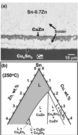
but the most reactive, constituent in SnZn. Accordingly, the SnZn/Cu systems meet the two necessary conditions for mass spalling presented in the previous section. The massive spalling indeed occurs in the reaction between Sn0.7Zn and Cu, as shown in Fig. 3共a兲. A thin layer of Cu6Sn5 formed between the solder/Cu interface, causing the spalling of the CuZn from the interface.
The Sn-rich corner of the Sn-Zn-Cu isotherm at 250 ° C, redrawn according to the study of Chou and Chen,13 is shown in Fig.3共b兲. Notice that the molten Sn phase can be in two-phase equilibrium with Cu6Sn5, CuZn, or Cu5Zn8, which
depend mainly on the Zn concentration. Similar to the mechanism proposed for the SnAgCu/Ni system, such CuZn massive spalling is attributed to the depletion of the most reactive element 共Zn兲 in the solder. During the reaction, CuZn initially formed at the interface. As this compound grew thicker, more and more Zn atoms became incorporated into CuZn, and the Zn concentration in the solder decreased. When the Zn concentration decreased to such a level that CuZn was no longer in equilibrium with the solder, the
equi-FIG. 2.共a兲 Micrograph showing the interface of a solder joint by reflowing a 760m Sn3Ag0.6Cu solder ball on a 375m opening Ni pad. The reac-tion condireac-tions were 235 ° C for 20 min. No spalling had occurred as the residual Cu concentration was 0.57 wt. % according to Eq.共1兲.共b兲 Same as 共a兲 but the ball diameter was 500m. No spalling occurred as the residual Cu concentration was 0.52 wt. %.共c兲 Same as 共a兲 but the ball diameter was 300m. Spalling had occurred because the residue Cu concentration was only 0.27 wt. %.
FIG. 3.共a兲 Micrograph showing the massive spalling in a SnZn/Cu solder joint after reaction at 250 ° C for 10 min. The spalled layer was CuZn.共b兲 Sn-rich corner of the Sn-Zn-Cu isotherm at 250 ° C. This isotherm was redrawn based on the information determined by Chou et al.共Ref.13兲.
librium phase now became Cu6Sn5 and this phase nucleated
between CuZn and Cu, and the spalling of CuZn occurred. The analysis in this section can be extended to Zn-doped SnAg, SnCu, and SnAgCu solders, because Zn is the most reactive constituent in these solders. If the Zn doping is high enough, say, higher than about 0.7 wt. %, the initial com-pound at the interface will be Sn-Zn based comcom-pounds. Nev-ertheless, if the Zn concentration is very low, Cu-based in-termetallic compounds 共Cu6Sn5 and Cu3Sn兲 would be the
dominant phases at the interface. Recently, it was reported that, in the SnAgCu/Cu reaction, minor Zn addition into the solder was an effective method for reducing the growth rate of Cu3Sn, which was responsible for the formation of
detri-mental Kirkendall’s voids.14 When doping Zn to these sol-ders to avoid the formation of excessive Kirkendall’s voids, one must be careful not to exceed a certain maximum level, or massive spalling might occur. We estimate that this maxi-mum level is about 0.7 wt. % Zn. However, more studies are needed to obtain a more precise value.
C. Massive spalling in Pb5Sn/Cu
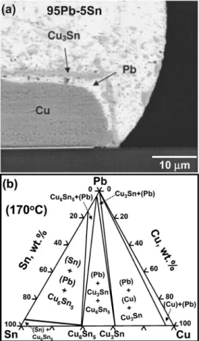
High Pb solders, such as Pb5Sn, are exempt from the EU RoHS requirements for flip-chip applications, and are ex-pected to be used in this area for an extended period of time in the future. Recently, it was reported that massive spalling could also occur in the Pb5Sn/Cu system.7,8 As will be shown below, the Pb5Sn/Cu system indeed exhibits the two necessary conditions for massive spalling pointed out in Sec. II A. One apparent difference is that, unlike SnAgCu/Ni and SnZn/Cu, where spalling occurred in the reflow stage when the solder were molten, spalling in Pb5Sn/Cu occurred in the aging stage when the solder was in the solid state. The reason for the occurrence of massive spalling in the solid state will be given below.
It is well known that only Cu3Sn forms when high-lead
PbSn solder is reacted with Cu.15,16 In the study of Jang et
al.,7the Cu3Sn layer formed during reflow, and adhered well to the interface after reflow. Spalling of Cu3Sn was not ob-served after 200 h of solid-state aging at 170 ° C, and only after 500 h of aging could spalling of Cu3Sn be observed.7 Shown in Fig. 4共a兲 is the microstructure of spalling after solid-state reaction at 170 ° C for 1000 h.7Jang et al. pointed out that spalling occurred because Sn near the interface had been consumed locally, and the diffusion of Sn in the solder was so slow that those Sn atoms far away from the interface could not diffuse back to the interface fast enough to keep the Sn concentration up. According to the Pb-Sn-Cu isotherm shown in Fig. 4共b兲, the local equilibrium at the interface changes from the Cu6Sn5+共Pb兲 two-phase field, to the
Cu3Sn+共Pb兲 phase field, then to the 共Cu兲⫹共Pb兲
two-phase field with decreasing Sn concentration. Therefore, spalling was again caused by the depletion of the most reac-tive constituent 共Sn in the present case兲 in the solder, al-though here the depletion occurred only locally near the in-terface. In fact, it had been shown in a follow-up study8that spalling would not occur in Pb10Sn/Cu diffusion couples subjected to the same treatment because the supply of Sn was more abundant.
The reason that spalling did not occur in the reflow stage was twofold. The number one reason was that the formation of Cu3Sn consumed relatively less Sn because the Cu/Sn
atomic ratio in Cu3Sn is 3:1. The formation of the Cu3Sn
layer did not significantly reduce the total amount of the available Sn atoms in Pb5Sn. The second reason is that Sn diffusion in the molten solder was much faster so that the Sn concentration near the interface never dropped below the level where Cu3Sn was no longer in equilibrium with the molten solder. Only in the solid state could the local Sn concentration near the interface drop below the level leading to mass spalling.
D. Massive spalling in Pb5Sn/Ni
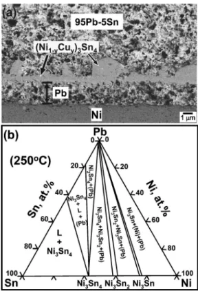
The Pb5Sn/Ni also exhibits the two necessary conditions for massive spalling, and massive spalling was indeed ob-served in this system.9 Figure5共a兲shows the massive spal-ling of Ni3Sn4after reaction at 350 ° C for 90 min,9and Fig. 5共b兲 shows the 250 ° C Pb-Sn-Ni isotherm calculated by Ghosh.17The Pb-Sn-Ni isotherm at 350 ° C is not available, but the 250 ° C isotherm should give a reasonable approxi-mation of the geometry of the phase relationships. Figure 5共b兲 shows that the equilibrium phase with 共Pb兲 changes from Ni3Sn4 to Ni3Sn2, and then to Ni3Sn, upon decreasing
the Sn concentration. Therefore, as more and more Sn atoms were incorporated into the growing Ni3Sn4, the Sn concen-FIG. 4. 共a兲 Micrograph showing the massive spalling in a Pb5Sn/Cu solder joint after aging at 170 ° C for 1000 h observed by Jang et al.共Ref.7兲. The spalled layer was Cu3Sn.共b兲 The Pb-Sn-Cu isotherm at 170 °C. The phase relations in this isotherm are from the study of Tu and Zeng共Ref.1兲.
tration decreased. Eventually the Sn concentration dropped to a level where Ni3Sn4was no longer stable at the interface, and the spalling of this compound occurred.
In contrast to the Pb5Sn/Cu reaction, mass spalling could occur during the reflow stage in the Pb5Sn/Ni reaction. The reason was that the growth of the reaction product Ni3Sn4 required a larger amount of Sn. The atomic ratio of
Ni/Sn was now 3:4. Even with this higher amount of Sn consumption, the reaction time had to be as long as 90 min to consume enough Sn to bring the Sn concentration down to the level required for massive spalling.
III. DISCUSSION
Despite several differences between the regular spalling and the massive spalling discussed in the previous sections, these two types of behavior do share one common feature in that they are all due to the exhaustion of a limiting constitu-ent. In regular spalling, it occurs after the exhaustion of the reaction layer of the substrate,1,2 and in massive spalling, it occurs when the reactive constituent in the solder falls below a certain level.
According to the arguments presented in Sec. II, several factors tend to favor the occurrence of mass spalling. The number one factor is the original composition of the reactive constituent of the solder关w0in Eq.共1兲兴. If this composition
is much greater than the threshold concentration required to change the equilibrium phase at the interface, then the mass spalling is less likely or will take a longer time to appear. This was indeed the case for the Pb5Sn/Cu reaction. In this case, the formation of Cu3Sn during reflow simply could not
lower the Sn concentration to the required level. The massive spalling could only occur during the aging stage when the diffusion of Sn in solid solder was slow.
The second factor that can influence massive spalling is the reflow time. The thickness of the compound at the inter-face grows with the reflow time, and according to Eq. 共1兲, the thicker the compound is at the interface, the larger is the drop in the concentration of the most reactive component. Therefore, the longer the reflow time is, the greater will be the chance for occurring massive spalling.
The third factor is the solder joint size. For industrial applications, it is typically djoint⬃1.2dpad. As a result, the
concentration drop is proportional to 1 / djoint, and will be
large for smaller djoint. In other words, smaller joints tend to
favor the occurrence of massive spalling.
The last factor is the existence of certain other coating layer on the substrate. For example, in the SnAgCu/Ni case, our preliminary study shows that a thin layer of Au over the Ni substrate tends to favor the occurrence of massive spal-ling. The reason for this Au effect is not clear at this moment, and a detailed study is underway to uncover this phenom-enon.
It should be emphasized that the arguments presented here are purely thermodynamic in nature. Nothing is said about dynamically how massive spalling occurs. In other words, we only identify the driving force for the massive spalling. The step-by-step mechanism is an important and extremely interesting area worthy of more studies. Without question, the interfacial energy must play an important role in “peeling” the intermetallic layer away from the interface.
IV. SUMMARY
A unified thermodynamic argument is presented to ratio-nalize the occurrence of the massive spalling in four different solder/substrate systems, including SnAgCu/Ni, SnZn/Cu, PbSn/Cu, and PbSn/Ni. The massive spalling occurs because, during reaction, the original reaction product at the interface is no longer in local thermodynamic equilibrium with the solder, and this compound is driving away to make room for the nucleation and growth of the equilibrium phase. Two necessary conditions for the occurrence of massive spalling are identified. The number one condition is that the reactive constituent must be present in a limited amount, and the second is that the soldering reaction must be very sensitive to the concentration of this element. Four factors are identified to favor the occurrence of the mass spalling: smaller initial concentration of the reactive constituent, longer reaction time, smaller joint size, and the presence of certain coating layer over the substrate.
ACKNOWLEDGMENTS
This work was supported by the National Science Coun-cil of R.O.C. through Grants No. NSC 95–2221-E-002–443-MY3 and No. NSC 95–2221-E-002–441. The authors also acknowledge the financial support of Siliconware Precision Industries Co.
1K. N. Tu and K. Zeng, Mater. Sci. Eng., R 34, 1共2001兲. FIG. 5. 共a兲 Micrograph showing the massive spalling in a Pb5Sn/Ni solder
joint after reaction at 350 ° C for 90 min observed by Wang and Chen共Ref. 9兲. The spalled layer was 共Ni1−yCuy兲3Sn4.共b兲 Pb-Sn-Ni isotherm at 250 °C. The phase relations in this isotherm are from the study of Ghosh共Ref.17兲.
2G. Z. Pan, A. A. Liu, H. K. Kim, K. N. Tu, and P. A. Totta, Appl. Phys. Lett. 71, 2946共1997兲.
3C. E. Ho, Y. W. Lin, S. C. Yang, C. R. Kao, and D. S. Jiang, J. Electron. Mater. 35, 1017共2006兲.
4C. E. Ho, S. C. Yang, and C. R. Kao, J. Mater. Sci. Mater. Electron. 18, 155共2006兲.
5L. C. Shiau, C. E. Ho, and C. R. Kao, Soldering Surf. Mount Technol. 14, 25共2002兲.
6S. C. Yang, C. E. Ho, C. W. Chang, and C. R. Kao, J. Mater. Res. 21, 2436 共2006兲.
7J. W. Jang, L. N. Ramanathan, J. K. Lin, and D. R. Frear, J. Appl. Phys. 95, 8286共2004兲.
8L. N. Ramanathan, J. W. Jang, J. K. Lin, and D. R. Frear, J. Electron. Mater. 34, 43共2005兲.
9K. Z. Wang and C. M. Chen, J. Electron. Mater. 34, 1543共2005兲. 10C. E. Ho, Y. L. Lin, and C. R. Kao, Chem. Mater. 14, 949共2002兲. 11C. E. Ho, R. Y. Tsai, Y. L. Lin, and C. R. Kao, J. Electron. Mater. 31, 584
共2002兲.
12W. T. Chen, C. E. Ho, and C. R. Kao, J. Mater. Res. 17, 263共2002兲. 13C. Y. Chou and S. W. Chen, Acta Mater. 54, 2393共2006兲.
14S. K. Kang, D. Leonard, D. Y. Shih, L. Gignac, D. W. Henderson, S. Cho, and J. Yu, J. Electron. Mater. 35, 479共2006兲.
15G. Z. Pan, A. A. Liu, H. K. Kim, K. N. Tu, and P. A. Totta, Appl. Phys. Lett. 71, 2946共1997兲.
16J. W. Jang, P. G. Kim, K. N. Tu, and M. Lee, J. Mater. Res. 14, 3895 共1999兲.