Influence of LT-GaN nucleation layer on the structural and optical properties
of MOVPE-grown a-plane GaN
Shih-Pang Chang
a,b, Hung-Chih Yang
b, Tien-Chang Lu
a,c,n, Hao-Chung Kuo
a, Shing-Chung Wang
aa
Department of Photonics & Institute of Electro-Optical Engineering, National Chiao Tung University, 1001 Ta Hsueh Road, Hsinchu 30050, Taiwan, ROC
bR&D Division, Epistar Co. Ltd., Science-based Industrial Park, Hsinchu 300, Taiwan, ROC c
Institute of Lighting and Energy Photonics, National Chiao Tung University, 301 Gaofa 3rd Road, Guiren Township, Tainan County, 711 Taiwan, ROC
a r t i c l e
i n f o
Available online 16 December 2009 Keywords:
A1. Nucleation layer A3. MOVPE A3. V/III ratio B1. GaN B2. Nonpolar
a b s t r a c t
The influence of the LT-GaN nucleation layer on the quality of the GaN template was investigated by the study of the surface morphology of the nucleation layer, and of the crystalline and optical properties of the subsequently grown a-plane GaN template. Both X-ray diffraction and photoluminescence results reveal that better crystalline and optical quality could be obtained using thinner nucleation layer thickness and higher V/III ratio, leading to brighter near band edge luminescence as compared to films grown on lower V/III ratio nucleation layer. Our experiments indicate that reduction in the density of nucleation layer islands can effectively improve the crystalline quality of a-plane GaN template, and the V/III ratio of nucleation layer is a more dominant growth parameter to improve the crystalline and optical quality at the same time. The optimized growth parameters for the nucleation layer in our study are thickness of 10 nm and V/III ratio of 9000.
Crown Copyright & 2009 Published by Elsevier B.V. All rights reserved.
1. Introduction
Nitride-based heterostructure devices grown in the polar [0 0 0 1] direction are affected by strong internal fields originating from strain-induced polarization and spontaneous polarization. These polarization fields have negative impact on the perfor-mance of light emitting devices. The quantum confined Stark effect (QCSE) results in the spatial separation of electrons and holes in quantum well structures with c-axis orientation, reduc-tion of oscillator strength, and red shift of the emission wavelength with excitation [1,2]. Nonpolar GaN and its alloys have attracted attention for use in optoelectronic device applictions due to the reduction of the polarization effect. Growth of a-plane GaN, in particular, has been extensively studied[3,4]. It is difficult to obtain high crystalline quality and smooth surface owing to high densities of stacking faults (SFs) and threading dislocations. Low temperature nucleation layers (NL) play a critical role in c-plane GaN growth[3], as they provide adequate nucleation sites for subsequent epitaxial growth, and directly affect the microstructure and the surface morphology of the epilayers[4,5]. A smooth surface can be achieved by adjusting the NL growth conditions as well as the V/III ratio of the subsequently
grown GaN template [6,7]. However, unlike the c-plane case, direct growth of a-plane GaN on r-plane sapphire results in high density of SFs and threading partial dislocations[8].
In order to minimize the defect density, it is essential to optimize the NL growth parameters such as thickness and V/III ratio. Although the structural and morphological characteristics of both a-plane and m-plane GaN have been widely studied, the relationship between crystalline and optical properties of non-polar III-nitride has not been well understood[9,10]. In this work, the effects of thickness and V/III ratio of the NL for a-plane GaN grown on r-plane sapphire were investigated.
2. Experiments
Si-doped a-plane GaN was grown on 430-
m
m-thick r-plane sapphire substrates in a low-pressure MOVPE reactor. Trimethyl-gallium (TMGa), ammonia and monosilane were used as pre-cursors. First, a low-temperature GaN NL was grown at 450 1C and 600 mbar with different V/III ratios and growth times. The growth conditions of the NL are shown inTable 1; there are two values of V/III ratio and thickness, which are 4000, 9000 and 10 nm, 30 nm, respectively. The increase in V/III ratio was achieved by increasing the ammonia flow while keeping the TMGa flow rate constant. After growing the NL, these films were coalesced at a low V/III ratio of about 500 at 970 1C and 100 mbar. The 2-m
m-thick template was then deposited at a rate of 2m
m/h, and the V/III ratio for the subsequently grown a-plane GaN template is aboutARTICLE IN PRESS
Contents lists available atScienceDirect
journal homepage:www.elsevier.com/locate/jcrysgro
Journal of Crystal Growth
0022-0248/$ - see front matter Crown Copyright & 2009 Published by Elsevier B.V. All rights reserved. doi:10.1016/j.jcrysgro.2009.11.059
n
Corresponding author at: Department of Photonics & Institute of Electro-Optical Engineering, National Chiao Tung University, 1001 Ta Hsueh Road, Hsinchu 30050, Taiwan, ROC. Tel.: + 886 3 5712121; fax: + 886 3 5716631.
E-mail addresses: [email protected] (T.-C. Lu), [email protected] (H.-C. Kuo).
ARTICLE IN PRESS
516. Samples with only NLs were also prepared with only LT-GaN growth at 450 1C and annealing at 970 1C, in order to observe the NLs used to grow the main high temperature GaN layer. The crystalline quality and surface morphology were characterized by X-ray diffraction (XRD) and atomic force microscopy (AFM), respectively. Room temperature photoluminescence (PL) measurements were performed using a CW 325 nm He–Cd laser operating at an excitation level of 25 mW (140 W cm 2) to
investigate the luminescence properties of a-plane GaN. The spatially resolved cathodoluminescence (CL) was investigated at 300 K, and the image data were obtained by scanning electron microscopy (SEM).
3. Results and discussion
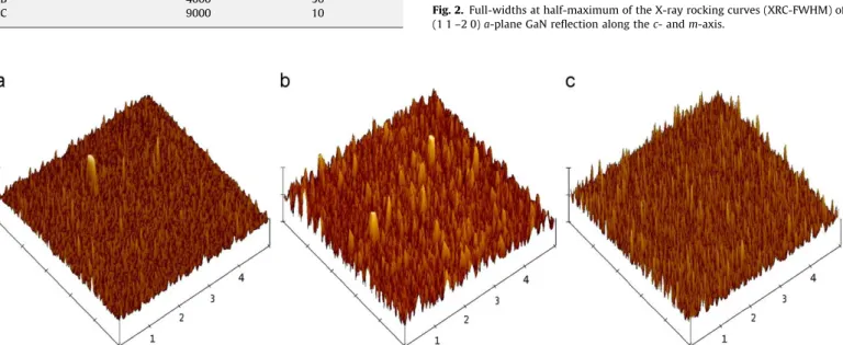
At first, we examined the surface morphologies of the un-coalesced GaN NL grown on r-plane sapphire in the conditions listed inTable 1.Fig. 1shows the AFM images of three kinds of growth conditions of NLs after annealing at 970 1C. The root mean square of the roughness for samples A, B and C is 0.73, 19.03 and 2.49 nm, respectively. For sample A, high-density nucleation of small GaN islands is observed, as shown inFig. 1(a). For sample B, as the NL thickness becomes thicker under the same V/III ratio, the island density is lowest and the grain size is largest among the three samples. The facet shape is more obvious than on the other two. For sample C, where 10 nm thick NL is grown under high V/III ratio, the island density is higher than that on sample B and the morphology is rougher than that on sample A as shown in
Fig. 1(c). Under the NL growth condition 30 nm thick and V/III
ratio 9000, there are lots of pits on the surface of subsequently grown a-plane GaN template, which is not shown here. This is not an appropriate growth condition of a-plane GaN on r-plane sapphire substrate.
Fig. 2shows the full width at half maximum (FWHM) of
high-resolution X-ray rocking curves (XRC) along [0 0 0 1] c and [1 1¯ 0 0] m directions (
p
= 01 and 901, respectively) for the 2-m
m-thick GaN layers grown on the different NLs described above. The XRC FWHM of a given a-plane GaN template in the [1 1¯ 0 0] direction was larger than that in the [0 0 0 1] direction for all three NL growth conditions. The strain along the orthogonal c and m crystal axes is quite different, and this will facilitate the formation of line defects[11]. From sample A to sample B, the XRD FWHM value decreases from 1741 to 959 arcsec for the [0 0 0 1] direction and from 803 to 695 arcsec for the [1 1¯ 0 0] direction. This indicates that the crystal quality becomes better as the NL thickness becomes larger. The lower density of NL islands reduces the density of grain boundaries, which will reduce the number of grain columns and results in lower RC-FWHM of the GaN template. The higher V/III ratio also decreased the value of XRC-FWHM from 1741 to 1049 arcsec for the [0 0 0 1] direction and from 803 to 605 arcsec for the [1 1¯ 0 0] direction. We supposed that the higher V/III ratio promotes 3D growth of the nuclei and results in lower density of islands than on sample A, which can reduce the mosaic structure in the GaN films.
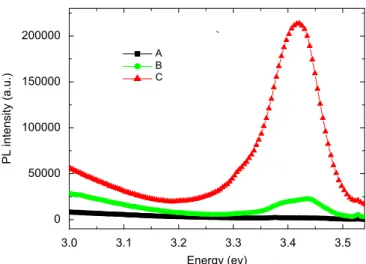
Because of the high density of stacking faults (SFs), no donor-bound exciton emission (at 3.465 eV)[12,13] is observed in PL spectra for any of the three samples. The emission of 3.41 eV is assumed to be due to near band edge emission (NBE). The higher density of SFs is accompanied by higher partial dislocation density
Table 1
The nucleation layers (NLs) growth conditions on r-sapphire substrate. NL growth condition V/III ratio Thickness (nm) A (reference) 4000 10
B 4000 30
C 9000 10
Fig. 1. Bird’s-eye-view AFM images of the NL after annealing at 970 1C. The NL was grown in: (a) condition A, (b) condition B and (c) condition C. A 400 600 800 1000 1200 1400 1600 1800 2000 2200 XRC FWHM (arcsec) sample number c-axes m-axes (1120) B C
Fig. 2. Full-widths at half-maximum of the X-ray rocking curves (XRC-FWHM) of (1 1 –2 0) a-plane GaN reflection along the c- and m-axis.
S.-P. Chang et al. / Journal of Crystal Growth 312 (2010) 1307–1310 1308
ARTICLE IN PRESS
and by weaker NBE emission. Therefore the stronger NBE emission intensity represents lower SF density, and higher optical quality. Sample A with NL thickness of 10 nm grown with a V/III ratio of 4000 can be taken as reference. In Ref. [3], Wu et al. report that it is more difficult for SFs to extend to the surface of subsequently grown GaN of the NL is thinner[3]. The thinner NL consists of small crystal domains that are not large enough for the nucleation of SFs, which results in lower SF density. Samples B and C have similar crystalline quality, the higher V/III ratio during growth of the NL results in the highest NBE emission, as shown in
Fig. 3. From the PL results, we suppose that a higher V/III ratio
during growth of the NL can reduce the SF density in the subsequently grown thick a-plane GaN layer more effectively than a thicker NL thickness.
The surface morphology of the GaN template is better with smaller NL islands as shown inFig. 4(a) and (c), the larger NL islands result in large inverse pyramidal pits on the surface as shown inFig. 4(b). When NL islands are too large, more 3D shapes
appear, which is similar to the condition of sample B. At the beginning of a-plane GaN epitaxy, the growth follows a Volmer– Weber (VW) mode first and then follows a Frank–van der Merwe (FM) mode after most of the islands have merged. A thicker NL results in more 3D initial growth mode and this may be a major reason that produces inverse pyramidal pits on the template surface. Both higher thickness and higher V/III ratio for the NL can effectively improve the crystalline quality of a-plane GaN template. However, to obtain a smooth surface, the thicker NL thickness is not appropriate in a-plane GaN growth condition.
From the PL results inFig. 3, the NBE emission is stronger if the NL layer was thicker. Comparing the spatial CL images inFig. 4(d) and (e), we observe that the major difference originates from the luminescence domain size, which is related to the grain size of GaN. The strongest NBE emission in PL also can be connected with the spatial CL results. The NBE emission is higher when the NL was grown with the higher V/III ratio (9000). The growth condition of sample C can favor 3D NL islands formation with lower nuclei density, producing more intense spatial NBE luminescence as shown in the CL map of Fig. 4(e). From other reports, the lengthening of SFs can be initiated after some critical thickness of NL, such as thicker than 30 nm [3]. In our experiments, using an NL thickness smaller than 30 nm produces small nuclei that prevent SFs from lengthening further. The density of NL nuclei directly influences the crystalline quality, which indicates that the parameters chosen for the growth of the 3D NL islands shall be a more dominant growth parameter to improve the crystalline and optical quality at the same time.
4. Conclusion
In conclusion, smoothly coalesced and pit free a-plane GaN was grown on r-plane sapphire substrate by MOVPE. The influence of LT-GaN NL on the quality of GaN template was investigated by the study of surface morphology of the NL and of the crystalline and optical properties of subsequently grown a-plane GaN template. Both XRD and PL results reveal that better crystalline and optical quality could be obtained under the conditions of thinner NL thickness and higher V/III ratio. This indicates that thin NL nuclei can prevent SF propagation, but more 3.0 0 50000 100000 150000 200000 PL intensity (a.u.) Energy (ev) A B C 3.1 3.2 3.3 3.4 3.5 Fig. 3. Stacking faults emission in PL spectra taken from of a-plane GaN epilayers grown on r-sapphire substrates and NLs obtained in growth conditions A, B and C.
5um
[email protected] [email protected] 5um [email protected] 5um
Fig. 4. SEM and corresponding CL images of the a-plane GaN template grown on top of the NL. NL growth conditions (a, d) 10 nm NL V/III ratio 4000; (b, e) 30 nm NL V/III ratio 4000; (c, f) 10 nm NL V/III ratio 9000.
ARTICLE IN PRESS
3D shaped nuclei can prevent the dislocation propagation. The optimum growth conditions for the NL in our study are the thickness of 10 nm and the V/III ratio of 9000. Narrow XRD rocking curves with FWHM of 605 arcsec along the [0 0 0 1] direction were obtained. The PL results reveal that the higher V/III ratio during NL growth is more beneficial in increasing the emission intensity, which was consistent with XRD results. Similar results of CL mapping images also show more intense spatial luminescence. These experiments indicate that reduction in the density of NL islands can effectively improve the crystalline quality of a-plane GaN template, and the V/III ratio of NL is a more dominant growth parameter to improve crystalline and optical quality at the same time.
Acknowledgment
The authors are grateful to the National Science Council of the Republic of China, Taiwan, for financially supporting this research under Contract no. NSC 96-2221-E009-067.
References
[1] P. Waltereit, O. Brandt, A. Trampert, H.T. Grahn, J. Menniger, M. Ramsteiner, M. Reiche, K.H. Ploog, Nature (London) 406 (2000) 865.
[2] Y.J. Sun, O. Brandt, S. Cronenberg, S. Dhar, H.T. Grahn, K.H. Ploog, P. Waltereit, J.S. Speck, Phys. Rev. B 67 (2003) 041306.
[3] Z.H. Wu, A.M. Fischer, F.A. Ponce, T. Yokogawa, S. Yoshida, R. Kato, Appl. Phys. Lett. 93 (2008) 011901.
[4] M. Araki, K. Hoshino, K. Tadatomo, Phys. Status Solidi (c) 4 (2007) 2540. [5] M. Araki, N. Mochimizo, K. Hoshino, K. Tadatomo, Jpn. J. Appl. Phys. 46 (2007)
555.
[6] J.L. Hollander, M.J. Kappers, C. McAleese, C.J. Hunphreys, Appl. Phys. Lett. 92 (2008) 101104.
[7] X. Ni, Y. Fu, Y.T. Moon, N. Biyikli, H. Morkoc, J. Cryst. Growth 290 (2006) 166. [8] V. Jindal, J. Grandusky, M. Jamil, E. Irissou, F.S. Sandvik, K. Matocha, V. Tilak,
Phys. Status Solidi (c) 3 (2006) 1792.
[9] Z.H. Wu, A.M. Fischer, F.A. Ponce, B. Bastek, J. Christen, T. Wernicke, M. Weyeers, M. Kneissl, Appl. Phys. Lett. 92 (2008) 171904.
[10] P.P. Paskov, R. Schifano, B. Monemar, T. Paskova, S. Figge, D. Hommel, J. Appl. Phys. 98 (2005) 093519.
[11] H. Wang, C. Chen, Z. Gong, J. Zhang, M. Gaevski, M. Su, J. Yang, M.A.sif Khan, Appl. Phys. Lett. 84 (2004) 499.
[12] R. Liu, A. Bell, F.A. Ponce, C.Q. Chen, J.W. Yang, M.A. Khan, Appl. Phys. Lett. 86 (2005) 021908.
[13] J. Mei, S. Srinivasan, R. Liu, F.A. Ponce, Y. Narukawa, T. Mukai, Appl. Phys. Lett. 88 (2006) 141912.
S.-P. Chang et al. / Journal of Crystal Growth 312 (2010) 1307–1310 1310