Effect of atomic geometry on shot noise in aluminum quantum point contacts
J. Yao,1 Y.-C. Chen,2M. Di Ventra,3and Z. Q. Yang1,*1Surface Physics Laboratory (National Key Laboratory), Fudan University, Shanghai 200433, China
2Department of Electrophysics, National Chiao Tung University, 1001 Ta Hsueh Road, Hsinchu, Taiwan 30010, Republic of China 3Department of Physics, University of California, San Diego, La Jolla, California 92093-0319, USA
共Received 7 January 2006; revised manuscript received 20 March 2006; published 26 June 2006兲
We investigate the role of atomic geometry on shot-noise properties of aluminum atomic contacts using first-principles calculations. We study both the effect of atomic separation in the wire as well as the geometry of the contacts. We find that shot noise, as opposed to conductance, is very sensitive to atomic details. In particular, the Fano factor for the asymmetric contact structures is more than double that of the symmetric ones due to increased backscattering, and is within the experimental range. These results indicate that shot noise may be used as a tool to infer the atomic geometries of quantum point contacts.
DOI:10.1103/PhysRevB.73.233407 PACS number共s兲: 73.40.Cg, 73.40.Gk, 85.65.⫹h
Atomic point contacts can be made using, e.g., mechani-cally controllable break junctions 共MCBJ兲 or scanning tun-neling microscope 共STM兲 techniques.1 The obtained struc-tures have been extensively studied both experimentally1–4 and theoretically.5–12 One issue that has received much less attention is how steady-state current fluctuations 共shot noise兲13 are affected by the atomic configurations of nanos-cale junctions. This is an important aspect as, in general, the atomic geometry of nanoscale junctions is unknown. In ad-dition, shot noise provides additional information on the transport properties of these systems, such as energy distributions,14 kinetics of electrons,15 and correlations of electronic wave functions.16
Very few studies have focused on the role of atomic con-figurations on noise properties. For instance, Lagerqvist et al.17 have performed first-principles calculations of shot-noise properties of parallel carbon wires and found that the Fano factor is quite sensitive to the bonding structure of the wires. Chen and Di Ventra18have found that shot noise of Si atomic wires of different lengths oscillates as a function of atoms in the wire.
Shot noise is due to charge quantization13 and it is, in general, a nonlinear function of the external bias V.18,19For mesoscopic systems, shot noise has been related to the trans-mission coefficients Tn共in the eigenchannel basis, with n the channel index兲. For a two-terminal geometry in linear re-sponse, it can be expressed as13
S = 4兩V兩e3 h
兺
nTn共1 − Tn兲, 共1兲
where e is the electron charge. It is clear from this equation that a fully open 共or closed兲 conducting channel does not contribute to shot noise. It is customary to discuss the Fano factor defined as the ratio of shot noise to its Poisson value Sp= 2e具I典, where 具I典 is the average dc current,13
F = S/Sp=
兺
nTn共1 − Tn兲/
兺
nTn. 共2兲
An alternative expression for shot noise in terms of single-particle wave functions⌿EL,R共r,K储兲 of left- and
right-moving electrons has been derived in Ref. 18 共in atomic units兲, S =
冕
EFL EFR dE冏
冕
dR冕
dKI˜E,ELR冏
2 , 共3兲where I˜E,ELR=共⌿EL兲*ⵜ⌿ER−ⵜ共⌿EL兲*⌿ER; dR defines an element of the electrode surface and K储is the component of the
elec-tron momentum parallel to it. Here we have assumed that a positive bias is applied to the left electrode so that the local Fermi level of the right electrode EFR is higher than that of the left electrode EFL. Expression共3兲 allows us to calculate shot noise and Fano factor once the single-particle states of the system are known. The equivalence of Eqs.共3兲 and 共1兲 has been proven in Ref. 17 in the case in which the trans-mission probabilities Tnare extracted from the single-particle states with independent transverse momenta.
In this paper, we investigate the dependence of shot noise on atomic geometry using aluminum共Al兲 atomic contacts as a prototypical example. Aluminum has the valence configu-ration共3s23p1兲 making it thus more interesting than gold in terms of bonding formation and interference between differ-ent orbitals. Aluminum atomic contacts have also been stud-ied extensively in experiments.2–4,20–22It has been suggested that at least three orbitals contribute to the total conductance, even for the narrowest contacts.4,21–26Van den Brom and van Ruitenbeek27 have measured shot noise of Al contacts and have reported a Fano factor within the range 0.3–0.6.
A schematic of the system investigated is represented in Fig. 1. The first structure we study is a straight three-atom wire connected to four-atom square bases representing an Al共001兲 surface geometry 关see Fig. 1共a兲兴. The bases are then connected to bulk electrodes which are represented with a semi-infinite jellium model,24,25,28with interior electron den-sity close to the value of metallic aluminum共rs⬇2兲.24,25In this case, we investigate the role of bond stretching on shot noise. We then focus on the geometries of a single atom connected to two Al共001兲 bases 关symmetric structure, Fig. 1共b兲兴 and to one base only 关asymmetric structure, Fig. 1共c兲兴, respectively. The results show that when the contact varies from the symmetric structure to the asymmetric one, the
PHYSICAL REVIEW B 73, 233407共2006兲
Fano factor more than doubles with a comparatively small reduction in conductance 共⬃25%兲. The large Fano factor obtained in the asymmetric structure is within the experi-mentally observed range.27
The shot noise is evaluated using Eq.共3兲 with the station-ary scattering wave functions of the whole system calculated by solving the Lippmann-Schwinger equation iteratively to self-consistency. Exchange and correlation are included us-ing the static density-functional theory 共DFT兲 within the local-density approximation 共LDA兲.17,25,28 More details of the calculations can be found in the original papers in Refs. 17, 25, and 28. Note that since the quantum point contact is made of the same type of metallic atoms, dynamical 共viscos-ity兲 corrections to the static DFT-LDA conductance are ex-pected to be small, as in the case of gold quantum point contacts.29 The initial Al atomic bond length and the Al-jellium edge distance are taken as 5.4 a.u. 共1 a.u. ⯝0.529 Å兲 and 2.6 a.u., respectively.24,25,30All calculations are done at a bias of 0.01 V, i.e., in the linear regime.
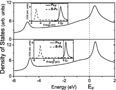
The calculated results for the geometries shown in Fig. 1 are given in Table I. The structure of Fig. 1共a兲 has a conduc-tance of 1.12G0 共G0= 2e2/ h兲 and a Fano factor of 0.09. In order to understand these values, we plot in Fig. 2共top panel兲 the density of states 共DOS兲 of this structure with the pro-jected density of states共PDOS兲 of the central atom 共inset兲. The first peak at about −4.9 eV is mainly due to s states while the second at about 0.4 eV comes from the px,y states, respectively. As the valence configuration of Al is共3s23p1兲, the wire structure has achannel having the characters of s and pz orbitals,6 and two degenerate channels with p
x,y character.25 For the p
x,y channels, similar to the analysis in
Refs. 28 and 31, we note that the contribution to the conduc-tance of a given resonant mode is approximately G0⫻DOS共EF兲/DOS共Epeak兲, where DOS共Epeak兲 is the peak value of the line shape of the corresponding resonance, and DOS共EF兲 is the corresponding quantity at the Fermi level. 共Since we are treating only the linear-response case, left and right Fermi levels have similar DOS.兲 Following this argu-ment, the conductance is mainly contributed from the px,y channels共see the PDOS of the px,ychannels in the inset兲. The s-pzchannel, on the other hand, has a very small contribution to the transmission. As a result the noise is suppressed.
We now discuss the effect of stretching the wire on con-ductance and noise. We stretch the atomic wire along the z axis with an increase in Al-Al bond length of ⌬l=0.4 a.u.. The conductance slightly decreases to 1.08G0, while the Fano factor is further suppressed to 0.03 共see the column with label “共a兲-s” in Table I兲. The plotted DOS in Fig. 2 共bottom panel兲 shows a narrower resonant peak above the Fermi levels. This narrowing is due to decreasing interac-tions between neighboring atoms. From the PDOS of the central atom in the inset, this narrowing thus reduces the ratio DOS共EF兲/DOS共Epeak兲 in px,y states, resulting in a re-duction of transmissions in the two degenerate channels.
To better understand this trend, we compare the local den-sity of states 共LDOS兲32 of the unstretched 共top panel兲 and stretched共bottom panel兲 wires in Fig. 3. We denote the at-oms in the wire as 1, 2, and 3 from left to right. We see that, by stretching the wire, the LDOS of the px,y orbitals de-creases, which is well demonstrated around the central atom. In particular, there is less overlap of the px,yorbitals between neighboring atoms共see, for instance, the bond structure be-tween atoms 2 and 3兲. On the other hand, the LDOS of the s-pz orbitals increases, which is evidently seen from the figures.33 The decrease 共increase兲 of LDOS for the px,y 共s-pz兲 orbitals implies a redistribution of transmissions be-tween these channels. The stretched wire has thus an almost
TABLE I. The calculated Fano factors and conductances corre-sponding to different structures depicted in Figs. 1共a兲–1共c兲. The label “共a兲-s” corresponds to the stretched three-atom wire structure of共a兲.
Structure 共a兲 共a兲-s 共b兲 共c兲
Conductance共G0兲 1.12 1.08 4.11 3.16
Fano factor 0.09 0.03 0.13 0.33
FIG. 1. Schematic of Al quantum point contacts connected to bulk electrodes 共gray blocks兲: 共a兲 a straight three-atom Al wire structure connected to four-atom square bases;共b兲 a central atom sandwiched between two square bases; 共c兲 a pyramid structure without the left square base.
FIG. 2. Top panel: density of states of the unstretched wire of Fig. 1共a兲. Bottom panel: density of states of the same stretched wire 共see text兲. We denote the left Fermi level as EF, and set it as zero of
energy. The insets are the projected densities of states of the central atoms in the unstretched and stretched wires.
BRIEF REPORTS PHYSICAL REVIEW B 73, 233407共2006兲
perfectchannel and less character from partially open px,y channels, thus further suppressing the shot noise关see Eq. 共1兲兴 compared to the unstretched one.
Let us now move on to the case in which we vary the contact geometry. We illustrate this in Figs. 1共b兲 and 1共c兲. The symmetrical structure of the contact关Fig. 1共b兲兴 produces a conductance of 4.11G0with a Fano factor of 0.13 as shown in Table I. Compared with the three-atom wire structure, the conductance and Fano factor both increase. The DOS of this structure is shown as a solid line in Fig. 4. The sharp peaks disappear and broaden to wide and smooth ones due to the strong interactions between the electrodes and the sample atoms. This feature indicates the disappearance of the quasi-one-dimensional character.34The Fermi level is now located near the peaks of the px,ystates. Therefore, the conductances
contributed from these states are quite substantial, as op-posed to the three-atom wire case. On the other hand, while the central atom in the three-atom wire structure makes con-tact directly along the z axis with neighboring atoms thus providing direct overlap of s, pzstates, there is no such direct overlap in the present case. The s-pz channel of the central atom thus weakens. The weakening of such a channel is, however, compensated for by the next-neighbor interaction26 between the two square bases. From the LDOS of the struc-ture in Fig. 5共left panel兲, it is clear that the interaction be-tween those base atoms is mostly of type.
Removing the left square base, we form an asymmetric structure 关see Fig. 1共c兲兴. The conductance of this structure decreases to 3.16G0 while the Fano factor is enhanced to 0.33 共Table I兲. This reduction in conductance is roughly in agreement with the decrease in DOS at the Fermi level25,28 共see Fig. 4, dashed line兲. However, the shape of the DOS is quite similar to the one of the symmetric structure, which indicates that the weight of the different types of orbitals does not vary substantially at each energy. The uniformity of the left electrode without base yields less directional spatial LDOS, thus decreasing the interactions between the right square base and the left jellium electrode. This is evident in the LDOS of this structure as plotted in Fig. 5共right panel兲. Unlike the -like interactions between these base atoms in the symmetric structure共Fig. 5, left panel兲, the right base in the asymmetric structure mainly interacts with the central atom, reducing the hopping between the left electrode and the right base. The breaking of symmetry between the right and left electrodes thus introduces additional backscattering, which reduces the conductance and introduces additional noise with a consequent increase in the Fano factor. The calculated Fano factor for this asymmetric structure is within the range of experimental data as reported in Refs. 20 and 27. We have also calculated the shot noise and conductance for structures with Al共111兲 surface orientations, and found the same trend. The behavior may indicate that Al atomic contacts fabricated using the MCBJ method1 may lack ide-ally symmetric neck structures. This behavior is consistent with the result of final breaking geometries of Al junctions obtained with total energy calculations.35
In conclusion, we studied the geometrical effects on shot-noise properties of two common types of Al atomic contacts. Our study revealed that shot noise is more sensitive to atomic arrangements than the conductance itself. The results
FIG. 3. LDOS of the unstretched共above兲 and stretched 共below兲 wires共insets show schematic of the wires and the plane where the LDOS is calculated兲. The black circles indicate the positions of the three atoms. The deep gray regions with dashed lines near the right electrode indicate lower charge density. The contour spacings of the LDOS are the same in both plots.
FIG. 4. Density of states of the symmetric共solid line兲 and asym-metric 共dashed line兲 structures 关see Figs. 1共b兲 and 1共c兲, respectively兴.
FIG. 5. 共Color online兲 LDOS of the symmetric 共left兲 and asym-metric共right兲 structures 共insets show schematic of the wires and the plane where the LDOS is calculated兲. The dark vertical lines indi-cate the surfaces of the jellium electrodes and the black circles denote the positions of the atoms.
BRIEF REPORTS PHYSICAL REVIEW B 73, 233407共2006兲
therefore indicate that shot noise may provide a tool to infer atomic configurations in atomic-scale junctions.
This work is supported by the U.S. National Science Foundation Grant No. DMR-01-33075, the Chinese
National Science Foundation Grant No. 10304002, Grand Foundation of Shanghai Science and Technology 共05DJ14003兲, PCSIRT, the Fudan High-End Computing Centre, and the Grant No. NSC 95-2112-M-009-024 from Taiwan National Science.
*Email address: [email protected].
1See, e. g., N. Agraït, A. L. Yeyati, and J. M. van Ruitenbeek, Phys. Rep. 377, 81共2003兲, and references therein.
2J. I. Mizobata, A. Fujii, S. Kurokawa, and A. Sakai, Phys. Rev. B 68, 155428共2003兲.
3A. Halbritter, Sz. Csonka, O. Yu. Kolesnychenko, G. Mihály, O. I. Shklyarevskii, and H. van Kempen, Phys. Rev. B 65, 045413 共2002兲.
4E. Scheer, N. Agraït, J. C. Cuevas, A. L. Yeyati, B. Ludoph, A. Martín-Rodero, G. R. Bollinger, J. M. van Ruitenbeek, and C. Urbina, Nature共London兲 394, 154 共1998兲.
5G. Taraschi, J. L. Mozos, C. C. Wan, H. Guo, and J. Wang, Phys. Rev. B 58, 13138共1998兲.
6J. C. Cuevas, A. L. Yeyati, and A. Martín-Rodero, Phys. Rev. Lett. 80, 1066共1998兲.
7Y. Fujimoto and K. Hirose, Phys. Rev. B 67, 195315共2003兲; K. Hirose, N. Kobayashi, and M. Tsukada, ibid. 69, 245412共2004兲. 8Y.-C. Chen and M. Di Ventra, Phys. Rev. Lett. 95, 166802
共2005兲.
9M. Di Ventra, Y.-C. Chen, and T. N. Todorov, Phys. Rev. Lett. 92, 176803共2004兲.
10N. D. Lang, Phys. Rev. B 55, 4113共1997兲.
11Z. Yang, M. Chshiev, M. Zwolak, Y.-C. Chen, and M. Di Ventra, Phys. Rev. B 71, 041402共R兲 共2005兲.
12Y.-C. Chen, M. Zwolak, and M. Di Ventra, Nano Lett. 3, 1691 共2003兲; 4, 1709 共2004兲; 5, 621 共2005兲.
13For a review, see Ya. M. Blanter and M. Büttiker, Phys. Rep. 336, 1共2000兲.
14O. M. Bulashenko, J. M. Rubí, and V. A. Kochelap, Phys. Rev. B 62, 8184共2000兲.
15R. Landauer, Nature共London兲 392, 659 共1998兲.
16T. Gramespacher and M. Büttiker, Phys. Rev. Lett. 81, 2763 共1998兲.
17J. Lagerqvist, Y.-C. Chen, and M. Di Ventra, Nanotechnology 15, S459共2004兲.
18Y.-C. Chen and M. Di Ventra, Phys. Rev. B 67, 153304共2003兲. 19Y. Wei, B. Wang, J. Wang, and H. Guo, Phys. Rev. B 60, 16900
共1999兲.
20H. E. van den Brom and J. M. van Ruitenbeek, Phys. Rev. Lett. 82, 1526共1999兲.
21J. C. Cuevas, A. Levy Yeyati, A. Martín-Rodero, G. R. Bollinger, C. Untiedt, and N. Agraït, Phys. Rev. Lett. 81, 2990共1998兲. 22E. Scheer, P. Joyez, D. Esteve, C. Urbina, and M. H. Devoret,
Phys. Rev. Lett. 78, 3535共1997兲.
23S. Okano, K. Shiraishi, and A. Oshiyama, Phys. Rev. B 69, 045401共2004兲.
24N. Kobayashi, M. Aono, and M. Tsukada, Phys. Rev. B 64, 121402共R兲 共2001兲.
25N. D. Lang, Phys. Rev. B 52, 5335共1995兲; N. D. Lang and M. Di Ventra, ibid. 68, 157301共2003兲.
26J. J. Palacios, A. J. Pérez-Jiménez, E. Louis, E. SanFabián, and J. A. Vergés, Phys. Rev. B 66, 035322共2002兲.
27H. E. van den Brom and J. M. van Ruitenbeek, in Statistical and
Dynamical Aspects of Mesoscopic Systems, edited by D.
Reguera, G. Platero, L. L. Bonilla, and J. M. Rubí 共Springer-Verlag, Berlin, 2000兲, p. 114.
28M. Di Ventra and N. D. Lang, Phys. Rev. B 65, 045402共2001兲; Z. Yang, A. Tackett, and M. Di Ventra, ibid. 66, 041405共R兲 共2002兲.
29N. Sai, M. Zwolak, G. Vignale, and M. Di Ventra, Phys. Rev. Lett. 94, 186810共2005兲.
30N. D. Lang, Phys. Rev. B 49, 2067共1994兲.
31N. D. Lang and Ph. Avouris, Phys. Rev. B 64, 125323共2001兲. 32The LDOS is the difference between the local density of states of
the complete system and the bare electrodes. It is integrated between the right and left Fermi levels.
33Note that the density between atoms 2 and 3 along the z direction in the stretched wire is higher than that in the unstretched one, although there are more contour lines around the middle point between atoms 2 and 3 for the unstretched wire. The contribu-tion from the s-pzstates decreases when approaching the middle
point in the unstretched wire, as opposed to the stretched one. 34T. Ono and K. Hirose, Phys. Rev. B 70, 033403共2004兲. 35P. Jelínek, R. Pérez, J. Ortega, and F. Flores, Phys. Rev. B 68,
085403共2003兲.
BRIEF REPORTS PHYSICAL REVIEW B 73, 233407共2006兲