Pergamon
Solid-Store Ekcrronics Vol. 39. No. 5. pp. 645451, 1996 Copyright (0 1996 Elsevier Science Ltd Printed in Great Britain. All rights reserved 0038-I 101196 $15.00 + 0.00
EFFECT
OF GE INCORPORATION
ON THE
PERFORMANCE
OF P-CHANNEL
POLYCRYSTALLINE
Si, _ .\Ge, THIN-FILM
TRANSISTORS
H. C. LIN’, H. Y. LIN* and C. Y. CHANG’
’ National Nano Device Laboratory, and ‘Institute of Electronics, National Chiao-Tung University. Hsin-Chu, 300 Taiwan, R.O.C.
(Received 18 June 1995; accepted 14 August 1995)
Abstract-In this study, p-channel polycrystalline silicon-germanium thin-film transistors (poly-Si, _ ,Ge, TFTs) with different Ge contents in the channel layer were fabricated and characterized. A novel device process was developed to fabricate the test samples. The device structure utilized the in situ boron-doped poly-Sk8Gc0 II with an extremely low resistivity (below 2 mR cm) as the source/drain and the undoped poly-Si (or Si, _,Ge,) as the channel layer. It is observed that the addition of Ge atoms in the channel would significantly increase the amount of trap density at grain boundaries thus degrading the device performance. Based on these results, we recommend the use of poly-Si, xGex source/drain to reduce the contact resistance but do not recommend that it is appropriate to replace poly-Si as the channel material of TFTs.
1. INTRODUCTION
Recently, it was shown by several groups[l-101 that the use of polycrystalline silicon-germanium (poly-Si, _ .yGe,) instead of polycrystalline silicon (poly-Si) would significantly reduce the thermal bud- get of device fabrication. This material has also been utilized for fabricating polycrystalline thin-film tran- sistor (TFTs) below 6OO”C[3,7-lo], showing its potential on the application of active-matrix liquid crystal display (AMLCD) manufacturing. However, these completed devices did not exhibit acceptable performance as comparing to the poly-Si ones thus preventing them from practical usage. In the work of Cao et a1.[9], they used a low pressure chemical vapor deposition (LPCVD) technique to prepare the poly films and explored the nature of gap states in a hydrogenated poly-Si,,,Ge,,, film. Their results showed that the poly-Si,,,Ge,,, was with a much higher density of gap states than the poly-Si. This led to the degraded device characteristics and was correlated to the lower H-passivation efficiency of Ge dangling bonds, smaller grain size of poly- Si,,8Ge0,2 as well as the higher impurity (e.g. 0) concentrations contained in the films.
In the present study, we used a novel approach, ultra-high vacuum chemical vapor deposition (UHV/ CVD), to deposit the poly-Si and poly-Si, _ ,Ge, films and investigated the effect of Ge content on the TFT performance. The ultra-high vacuum chemical vapor deposited poly films are different from those grown using LPCVD with the following properties.
(i) The films are with stable fine grains when deposited at a temperature as low as 550°C
(ii)
(iii)
(iv)
[2,3.11,12] and no recrystallizing treatment is required to transform them into the poly- crystalline state.
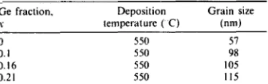
Grain size of the deposited poly-Si, .Ge, films is larger than that of poly-Si ones[12] (see Table l), which is in contrast to the samples used in the previous work[9].
The base pressure of this UHVjCVD system is about IO-* torr which is four orders lower than that of LPCVD approach. Such a condition ensures a minimal impurity contamination during deposition[ 11,131.
No hydrogenation step was used in this study, so the “intrinsic” properties of the deposited films can be probed.
Meanwhile. in order to get a more clear conse- quence between the incorporated Ge content in the channel layer and the resulted device performance, we fabricated TFTs with several different Ge contents.
2. DESCRIPTION OF THE UHV/CVD TECHNIQUE FOR DEPOSITING THE POLY FILMS
The UHVjCVD system consists of a growth chamber and a load-lock chamber[2,13]. The load- lock chamber is made of stainless steel while the growth chamber is a quartz tube of 6-inch in dia- meter, which is capable of 3- to 5-inch Si multi-wafer processing. These two chambers are connected by a gate valve and pumped down separately by their own turbo pumps, which are back supported by mechan- ical pumps. The pumping speeds of the turbo pumps are 1300 l/s-’ and 150 l/s-’ for growth chamber and load-lock chamber, respectively. The base pressure in
Table I. Grain size of the undoped poly films’
Ge fraction. Deposition Grain size
.x temperature ( C) (nm)
0 550 51
0.1 550 98
0.16 550 105
0.21 550 II5
*Film thickness of the measured samples is around 200 nm.
the growth chamber is maintained at about 2 x
lo-' torr which contains 0, and H,O less than 10e9 and 5 x 10m9 torr, respectively, as investigated by the residual gas analyzer (RGA)[13]. Under such a low background pressure, we have found that the oxygen and carbon concentrations in the grown films were
below the detection limit of secondary ion mass spectroscopic (SIMS) measurement, which is about 10” and lO”cm- for oxygen and carbon, respect- ively. In the standby state, the tube temperature was kept at 550°C all the time.
The flow rates of the reaction gases were controlled by their own mass flow controllers (fully metal-sealed type, TYLAN FC-780 MFC). Pure silane (SiH,) and 10% germane (GeH,) in H, was used as the source gases for Si and Ge, respectively, while 1% or 100 ppm B, H, in H, was used as the doping gas. Each MFC is interfaced to a personal computer for a flexible growth process control via automation.
In this work, the poly films were deposited on 3-inch Si wafers coated with a thermally grown oxide layer. Prior to deposition, the wafers were cleaned in a mixture of H2S0,/H202 (3 : 1) for 15 min, followed by a 5 min deionized water rinse. Substrates were then blown dry with nitrogen gas and put on a quartz boat inside the loading chamber. After this step, the
load-lock chamber was pumped down to a level below 2 x 10m6 torr normally within 30 min. Then, the gate valve was open and the wafers were trans- ferred into the growth chamber via a magnet-coupled linear/rotatory transfer rod. During the transferring process, a hydrogen flow of 600 seem was introduced into the growth chamber to suppress the contami- nation from the load-lock chamber.
3. MATERIAL PROPERTIES
With the aforementioned growth conditions, we have demonstrated in our previous publications [2,3,11,12] that this technique is capable of producing both poly-Si and poly-Si, _.rGe_V films with stable fine grains. As Ge atoms were incorporated, the peak locations of X-ray diffraction (XRD) spectra shifted to lower angle values and the amount of shift increased with increasing Ge content. This indicated that Ge incorporated uniformly. Additionally, the undoped poly-Si, _,VGe, films were found to be with a larger grain size than poly-Si[l2] (see Table 1) owing to the high surface mobility of Ge atoms during deposition.
We have also studied the characteristics of boron- doped poly-Si, _,Ge, films. The results showed that the resistivity of deposited films grown at 550°C can be lower than 2mQ cm without further annealing treatment. This is due to the non-equilibrium doping effect[l,2], that is, the effective carrier concentration contained in the films is higher than the solid solubil- ity of dopant. This effect can be resolved with the XRD technique. Figure 1 shows the XRD spectra done on the poly-Si,,79Ge,-,2, film grown at 550°C with
40 50 60
2Theta
YRD spectra of a non-equilibrium boron-doped poly-Si,,,,Ge,,, film with a carrier concentration of 4.8 x 10” cm-3: (a) the as-deposited film and (b) after a 900°C I-h anneal.
Effect of Ge incorporation on the performance of p-channel polycrystalline Si, _ ,Ge, thin-film transistors 641
a boron concentration of about 2 x lo*’ crnm3 before and after a 900°C l-h annealing. It is observed that the peak positions shift to the lower 20 values after the annealing treatment, implying that the lattice constant is expanded. This is a reasonable result. Under the non-equilibrium doping state, the boron atoms which occupy the substitutional sites of Si, _.Ge, lattice would result in a smaller average lattice constant because of its smaller covalent radius as compared with those of Si or Ge atoms. Hall measurements showed that the hole concentration decreased from 4.8 x 10” cmm3 for this as-deposited poly-Si,,,,Ge, 21 film to 1.2 x 1020cm-3 after an above-mentioned high-temperature treatment. After the annealing step, the non-equilibrium boron atoms would precipitate and lead to a larger lattice constant observed in Fig. 1. To our knowledge, this is the first time that the non-equilibrium effect for poly films is clearly identified with the XRD method.
Such low resistivity of in situ boron-doped poly- Si, _ ,Ge, makes it a potential candidate for low- temperature device fabrication. This way can replace the conventional ion-implantation method to ehmin- ate the long-term activation step. In order to utilize this advantage, we proposed the use of poly-Si/poly- Si, _,Ge, multi-layers and developed a novel process presented in the next section for TFT fabrication.
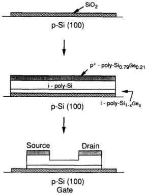
4. DEVICE FABRICATION AND CHARACTERIZATION
The main process steps for the proposed TFT process are illustrated in Fig. 2. Device structure is with a bottom-gate configuration. 3-inch p-type Si( 100) wafers were used as the starting materials and, for simplicity, as the gate electrode. A 60 nm-thick dry oxide layer was grown on the Si substrates and served as the gate dielectrics. Prior to deposition, the wafers were cleaned in a mixture of H2S0,/H202 (3: 1) for 15 min, followed by a 5 min rinse in D.I. water and then spun dry with nitrogen gas. Then, an i-Si, 1Ge,/i-Siip+-Si,,,Geo2, multilayer was de- posited sequentially on the gate oxide. All these layers were deposited at 550°C. The i-Si, _,Ge, was employed as the channel layer and four different Ge contents, namely. .Y = 0. 0.1, 0.16, and 0.21, were used for this study. In the mean time. the i-Si acted as a buffer layer for allowing P+-S~,,,~G~,,, to be etched selectively on. Thickness of the gate oxide is 60 nm. Other detailed structural parameters are given in Table 2. The p+-Si,,,,Ge,,,, layer is with carrier concentration and thickness of 4.8 x 10²”cm-3 and
p-Si (100)
P+ - PotY-Sio.zaGeo.21
p-Si (100) i - poiy-si, _:Ge,
Source Drain
p-Si (100)
Gate
Fig. 2. Process flow of the proposed poly-Si, _ ,Ge, TFT fabrication.
36 nm, respectively. The sheet resistance of the as- deposited films is 450 + 20 R/square. Cross-sectional TEM micrographs of the deposited i-Si/p + Si,,,Ge,,, and i-Si,,,Ge,,, ji-Si/p +-Si,,,,Ge,,,, are shown in Fig. 3(a, b), respectively. As can be seen in then two pictures that the one used for poly-Si TFT fabrication [Fig. 3(a)] is with a relatively smaller grain size as comparing to the other sample [Fig. 3(b)]. This is consistent with the observation shown previously[l2]. As a consequence, the undoped poly-Si, _ ,Ge, channel layers with a larger grain size would act as the seed for subsequentially grown undoped poly-Si layer, making the interface between the two unclear. The larger grain size also leads to the rougher surface morphology of the deposited films.
Following the film deposition, source and drain regions were defined by a photomask and then etched in a HNOj:CH3COOH:HF = 20:40: I solution. The etching rate ratio for boron-doped poly-Si, ,9Geo,z, with respect to undoped poly-Si films is over IO. After these steps. active regions were then defined by dry etching, and followed by low-temperature oxide (LTO) passivation, contact hole definition, and Al metallization steps. Finally, a 30-min sit-&ring
Table 2. Structural parameters for poly-Si and poly-Si, ,Ge, TFTs used in Fig. 2 My-Si, ,Ge, TFT Poly-Si TFT Gate oxide
Channel layer
Undoped poly-Si buffer layer P+ Dolv-Si, .Ge. Laver
60 nm 50 nm (J =O.l, 0.16. and 0.21) 200 nm 36 nm 60 nm 250 nm * 36 nm *The channel layer of poly-Si TFTs was also used as the undoped poly-Si buffer
Fig. 3. Cross-sectional TEM micrographs of (a) i-poly- Siip +-poly-Si,,gGe,2,, and (b) i-poly-Si, ,,Ge,,, /i-poly- Si/p +-poly-Si, ,,Ge, I1 multilayers deposited on a
60 nm-thick oxide layer.
treatment was given at 4OO”C, which is the highest temperature step after the deposition of poly films. Current-voltage characterization was performed using an HP4145B parameter analyser. It should be noted that throughout these processes stated above, no post treatments, such as recrystallization, post- ion-implantation annealing, or hydrogenation, were imposed on the films after deposition. Therefore, the intrinsic electrical properties of the as-deposited films can be evaluated directly via the performance of the completed devices.
5. RESULTS AND DISCUSSION
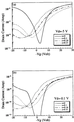
Typical drain current vs gate voltage characteristics exhibited by the four types of TFTs with different Ge contents in the channel layer are shown in Fig. 4. These measured devices are with identical -channel length and width of 140 and 120pm, respectively.
-vg (Volt)
lo.“t.“‘I”.\‘.I.“““““”
-20 -10Pvg ,vo,:p
20
Fig. 4. Subthreshold characteristics of TFTs with different Ge contents in the channel measured at (a) V,, = - 5 V and
(b) V,, = -0.1 V.
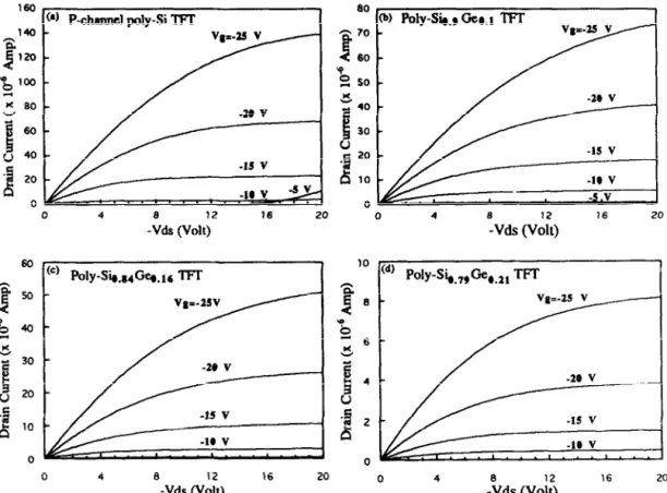
The drain voltages (V,,,) used are -5 and -0.1 V in Fig. 4(a, b), respectively. Output characteristics of these devices are shown in Fig. 5. The field effect mobility is evaluated in linear region at Vds = - 0.1 V with maximum transconductance. Detailed summary of these characteristics is given in Table 3.
The large amount of trapping states contained at the grain boundaries is essential in influencing the electrical characteristics of polySi films and makes the conduction behavior of poly-Si TFTs significantly different from that of Si MOSFETs[l4]. It is known that the carrier-trapping model[ 15-l 71 is a simple but
Table 3. Typical characteristics of the poly-Si and poly-Si, ,Ge, TFTs. The channel width and length are 120 and 140 pm,
resocctivelv Ge content in
channel (at.%) Threshold voltage (V)* Field effect mobility (cm2 v-1 s 1)’ Subthreshold swing ( V decade ’ )* On-off current ratio
0 10 16 21 - 11.6 - 1.6 - 12.6 - 16.7 I9 13 9 6 0.77 3 2.9 3.6 9 0.7 0.8 0.4 (x lovt
Density of trapping states (x lO”2mm~q’
5.3 9.8 10.7 12.6
*Measured at V,, = -0.1 V. tMeasured at Vdr = -5 V.
Effect of Ge incorporation on the performance of p-channel polycrystalline Si, _ ,Ge, thin-film transistors 649 140 ^a 4 120 $ 100 K 60 d i 60 CJ 40 d 2o 0 0 4 16 20 0 4 6 -Vds (V::f, 16 20 60
(a) Poly-Sii., Gee.1 TFr
-10 v 0 0 4 6 -vds ,v& 16 20
(d)
Poly-Si,,,Ge,.z, TFT -15 v 0 4 -eVds (Vozj 16 20Fig. 5. Drain current vs drain voltage characteristics for (a) poly-Si, (b) poly-Si,,,Ge, !, (c) poly-S&&e, ,h and (d) poly-Si,,Ge,,,, TFTs.
efficient way in describing the conduction behavior of carriers in polycrystalline materials. The potential barrier created by the trapping states is related to the difference in carrier concentration between the grains and the grain boundaries. For a TFT operation, the variation of gate voltage would modulate the carrier concentration inside the conduction channel and, thus, the barrier height at grain boundaries. Based on the method proposed by Levinson et a1.[18] and modified by Proano et a1.[19], we can estimate and compare the magnitude of the density of grain- boundary trapping states (N,) from the cur- rent-voltage characteristics.
Value of N, for the poly-Si TFT is about 5.3 x lOI* cm-‘. This is very close to the value shown in our previous study[20] (4.7 x lOI cm-*) which was extracted from the relationship between resistivity and carrier concentration using the carrier-trapping model. In Fig. 4, the poly-Si TFT exhibits an on/off current ratio of about lo6 at Vdr = -5 V and the maximum field-effect hole mobility of 19 cm* V- ’ s- ’ in the linear region evaluated at V,,, = -0.1 V. It should be noted that these electrical characteristics are difficult to be achieved for other approaches without any post-treatment. The superior device performance obtained by us is attributed to the high-quality poly films deposited with the UHV/CVD system. The magnitude of the field-effect mobility and the on-off current ratio have been found to be closely
related to the strain-bond tail states[21]. As men- tioned in Section 2 that the impurity levels, such as the oxygen and carbon atoms, contained in the deposited poly films were below the detection limit of SIMS measurement. This is in strong contrast tot that grown with conventional LPCVD techniques [9,22,23]. We believe that this low-level impurity contamination would result in a low density of tail states, which accounts for the high field-effect mobil- ity and high on-off current ratio achieved in this work.
On the other hand, the addition of Ge in the channel would introduce an additional amount of N,. The values of N, for poly-Si, _.,Ge, TFTs are around or higher than lOu cm-2. This implies that the Ge incorporation in the channel layer would degrade the device performance. As observed in Fig. 4 and Table 3, the subthreshold swing and on-off current ratio become worse for the TFT with a higher Ge content in the channel layer, This is obviously due to the larger amount of N, introduced with the Ge incorporation.
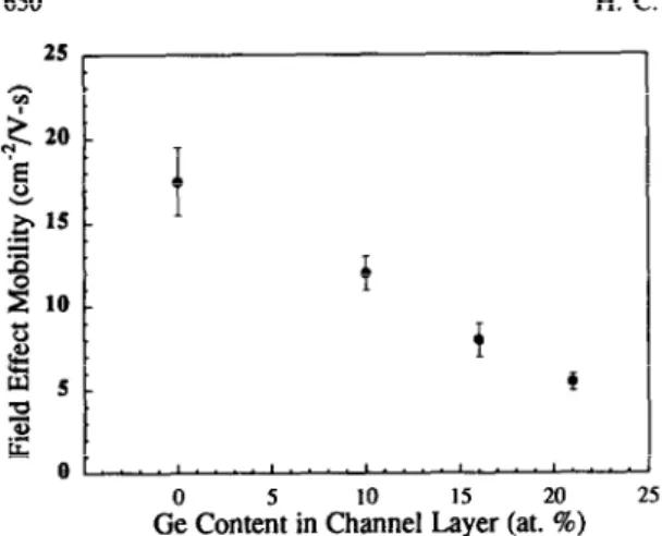
A similar trend also occurs to the case of field-effect mobility. This is seen in Fig. 6 in which the field-leffect mobility is shown as a function of Ge content in the channel layer. Over 20 devices were measured for each type of TFT to confirm this trend. Although the incorporation of Ce atoms would enlarge the grain size significantly, as shown in Fig. 3, but the
G”, Conkit in Ch’Zmel Zyer (at.‘;) 25 Fig. 6. Field-effect mobility of the completed TFT devices
as a function of the GE content in the channel layer.
field-effect mobility decreases with increasing Ge content owing to the higher N, value. These obser- vations indicate that the “intrinsic” material proper- ties of poly-Si, _ ,Ge, are not good enough to replace poly-Si as the channel layer of TFT devices. How- ever, the causes of more trapping centers for poly- Sir _,VGe, films are complicated since the alloy composition and require more investigations to un- derstand. More detailed identifications about the distribution of trapping states inside the gap using the field-effect conductance method are getting underway and will be presented in the next report.
The threshold voltage is defined as the intercept of linear drain current with the axis of gate voltage. Figure 7 plots the threshold voltage as a function of the channel Ge content. When the Ge atoms were incorporated, the absolute value increases with increasing Ge content. This is mainly related to the higher amount of N, contained in the device with a higher Ge content in the channel[24]. On the other hand, though the undoped poly-Si films are with a much lower N, value as compared with the poly- Si,_.Ge, ones, the absolute value of threshold voltage for poly-Si TFT is smaller than and compar- able to the poly-Si,,,Ge,, and poly-Si,,,Ge,,,, TFTs,
.201”““..““,‘1”“t”“1”‘.1
0 5 10 15 20 25
Ge Content in Channel Layer (at.%)
Fig. 7. Threshold voltage of the completed TFT devices as a function of the Ge content in the channel layer.
respectively. This observation is presumably caused by the different nature of oxide fixed charge between the two cases. Referring to several recent works [25,26], a considerable amount of negative fixed charge presented at the oxide/Si, _JGe, interface was identified using the capacitance-voltage (C-V) measuring technique. These charges are of opposite sign to that found at oxide/Si interface[27] would explain the results shown in Fig. 7.
6. CONCLUSIONS
In this report, we present a novei process for fabricating poly-Si and poly-Si, _,Ge, TFTs at low temperatures (below 55OC) and investigated the effect of Ge incorporation in the chaqnel layer on the performance of the completed devices. Our work reveals that the incorporation of Ge in the channel layer of polycrystalline TFTs would introduce a large amount of trapping states at the grain boundaries. This would degrade onoff current ratio, sub- threshold swing and field-effect mobility of the com- pleted devices. Our findings indicate that the poly-Si, _,Ge, films are not appropriate to be used as the channel layer.
Acknowledgements-The authors would like to thank Dr F. M. Pan for his helpful discussion. This work was supported by the National Science Council of Republic of China under contract No. NSC83-O417-EOO9-016.
REFERENCES
I. M. Sanganeria, D. T. Grider. M. C. Ozturk and J. J. Wortman, J. Elecctron. Mater. 21, 61 (1992).
2. H. C. Lin, H. Y. Lin, C. Y. Chang, T. F. Lei, P. J. Wang. R. C. Denn. J. Lin and C. Y. Chao. J. Aool.
#lysr;rl, 5395 (19ijj). Z1 3. H. C. Lin, T. G. Jung, H. Y. Lin, C. Y. Chang and L. P.
Chen, Appt. Phys. Lett. 65, 1700 (1994).
4. T. J. King, K. C. Saraswat and J. R. Pfiester, IEEE Elecwon Device Lett. 12, 533 (1991).
5. T. J. King, J. R. Pftester, J. D. Shott, J. P. McVittieand K. C. Saraswat, IEDM Tech. Dig. 253 (1990). 6. T. J. King and K. C. Saraswat, IEEE Electron Device
Len. 13, 309 (1992).
7. T. J. King and K. C. Saraswat, IEDM Tech. Dig. 567 (1991).
8. T. J. King, J. R. Pfiester and K. C. Saraswat, IEEE Electron Device Lett. 12, 584 (1991).
9. M. Cao, T. J. King and K. d. Saraswat, Appl. Phys. L&r. 61, 672 (1992).
10. S. Jurichich, T. J. King, K. C. Saraswat and J. Mehlhaff,
Japn. J. Appl. Phvs. 33, L1139 (1994).
I I. H. C. Lin, H. Y. Lin, C. Y. Chang, T. F. Lei, P. J. Wang and C. Y. Chao, Appt. Phys. Left. 63, 1351 (1993). 12. H. C. Lin, C. Y. Chang, W. H. Chen, W. C. Tsai, T. C.
Chang, T. G. Jung and H. Y. Lin, J. Electrochem. Sot. 141, 2559 (1994).
13. T. G. Jung, C. Y. Chang, T. C. Chang. H. C. Lin, T. Wang, W. C. Tsai. G. W. Huang and P. J. Wang,
Japn. J. Appl. Phys. 33, 240 (1994).
14. T. S. Li and P. S. Lin, IEEE Electron Device Lert. 14, 240 ( 1993).
15. T. 1. Kamins, J. Appl. Phys. 42, 4357 (1971). 16. J. Y. W. Seto, J. Appl. Phys. 46, 5247 (1975).
Effect of Ge incorporation on the performance of p-channel polycrystalline Si, _ ,Gev thin-film transistors 651
17. G. Baccarani, B. Ricco and G. Spadini, J. Appl. Phys.
49, 5565 (1978).
18. J. Levinson, F. R. Shepherd, P. J. Scanlon, W. D. Westwood. G. Este and M. Rider. J. ADDI. Phvs. 53.
1193 (198i). ._ _
19. R. E. Proano, R. S. Misage and D. G. Ast, IEEE Trans. Eleciron Device 36, 1915 (1989).
20. H. C. Lin, H. Y. Lin, C. Y. Chang, T. G. Jung, P. J. Wang, R. C. Deng and J. Lin, J. Appl. Phys. 76, 1572 (1994).
21. I. W. Wu, T. Y. Huang, W. B. Jackson, A. G. Lewis and A. Chiang, IEEE Electron Deoice Left. 12, 181 (1990).
22. T. J. King and K. C. Saraswat, J. Elecrrochem. Sot. 141, 2235 (1994).
23. T. I. Kamins and J. E. Turner, Solid-St. Technol. 80 (1990).
24. A. Ortiz-Conde and J. G. Fossum, IEEE Trans. Electron Device 33, 1563 (1986).
25. D. K. Navak. K. Kamioo. J. S. Park. J. C. S. Woo and K. L.-Wang, IEEE- Trans. Electron Detrice 39, 56 (1992).
26. P. W. Li and E. S. Yang, Appl. Phys. L.etr. 63, 2938 (1993).
27. S. M. Sze, Physics of Semiconductors Devices. 2nd edn. Wiley, New York (1981).