Effects of interfacial sulfidization and thermal annealing on the electrical properties of
an atomic-layer-deposited Al 2 O 3 gate dielectric on GaAs substrate
Chao-Ching Cheng, Chao-Hsin Chien, Guang-Li Luo, Chun-Hui Yang, Ching-Chih Chang, Chun-Yen Chang, Chi-Chung Kei, Chien-Nan Hsiao, and Tsong-Pyng Perng
Citation: Journal of Applied Physics 103, 074102 (2008); doi: 10.1063/1.2901167 View online: http://dx.doi.org/10.1063/1.2901167
View Table of Contents: http://scitation.aip.org/content/aip/journal/jap/103/7?ver=pdfcov Published by the AIP Publishing
Articles you may be interested in
Oxide scalability in Al 2 O 3 Ga 2 O 3 ( Gd 2 O 3 ) In 0.20 Ga 0.80 As Ga As heterostructures J. Vac. Sci. Technol. B 26, 1132 (2008); 10.1116/1.2884739
Atomic-layer-deposited Hf O 2 on In 0.53 Ga 0.47 As : Passivation and energy-band parameters Appl. Phys. Lett. 92, 072901 (2008); 10.1063/1.2883967
Interfacial self-cleaning in atomic layer deposition of Hf O 2 gate dielectric on In 0.15 Ga 0.85 As Appl. Phys. Lett. 89, 242911 (2006); 10.1063/1.2405387
Spectroscopic and electrical properties of atomic layer deposition Al 2 O 3 gate dielectric on surface pretreated Si substrate
J. Appl. Phys. 99, 074109 (2006); 10.1063/1.2187409
Surface passivation of III-V compound semiconductors using atomic-layer-deposition-grown Al 2 O 3 Appl. Phys. Lett. 87, 252104 (2005); 10.1063/1.2146060
Effects of interfacial sulfidization and thermal annealing
on the electrical properties of an atomic-layer-deposited Al
2O
3gate
dielectric on GaAs substrate
Chao-Ching Cheng,1Chao-Hsin Chien,1,2,a兲 Guang-Li Luo,2Chun-Hui Yang,2 Ching-Chih Chang,1Chun-Yen Chang,1 Chi-Chung Kei,3 Chien-Nan Hsiao,3 and Tsong-Pyng Perng4
1
Institute of Electronics, National Chiao-Tung University, Hsinchu, Taiwan 300, Republic of China 2
National Nano Device Laboratory, Hsinchu, Taiwan 300, Republic of China 3
Instrument Technology Research Center, National Applied Research Laboratories, Hsinchu, Taiwan 300, Republic of China
4
Department of Material Science and Engineering, National Tsing-Hua University, Hsinchu, Taiwan 300, Republic of China
共Received 15 September 2007; accepted 22 January 2008; published online 1 April 2008兲 In this study we investigated the interfacial chemistry occurring between an atomic-layer-deposited Al2O3high-k film and a GaAs substrate and the impact of sulfidization and thermal annealing on the properties of the resultant capacitor. We observed that sulfide passivation of the Al2O3/GaAs structure improved the effect of Fermi level pinning on the electrical characteristics, thereby providing a higher oxide capacitance, smaller frequency dispersion, and reduced surface states, as well as decreased interfacial charge trapping and gate leakage currents. Photoemission analysis indicated that the共NH4兲2S-treated GaAs improved the quality of the as-deposited Al2O3 thin film and preserved the stoichiometry of the dielectric during subsequent high-temperature annealing. This behavior was closely correlated to the diminution of GaAs native oxides and elemental arsenic defects and their unwanted diffusion. In addition, thermal processing under an O2 atmosphere, relative to that under N2, decreased the thickness of the Al2O3gate dielectric and relieved the gate leakage degradation induced by metallic arsenic; as a result, superior dielectric reliability was attained. We discuss the underlying thermochemical reactions that account for these experimental observations. © 2008 American Institute of Physics.关DOI:10.1063/1.2901167兴
I. INTRODUCTION
Presently, GaAs materials are used widely in such appli-cations as optoelectronic devices, photodiodes, high-electron-mobility transistors, and other high-frequency de-vices. In attempts to obtain superior performance rivaling or exceeding that of transistors on traditional Si-based sub-strates, various high-k gate dielectrics have been examined on high-mobility III-V substrates, especially GaAs- and InSb-based compound materials.1,2 Studies into competitive insulators on compound semiconductors and efficient passi-vation methods have been performed for more than four de-cades; the poor quality of the insulator-substrate interface has been the foremost obstacle hindering the realization of III-V metal oxide semiconductor 共MOS兲 devices. In addition to SiO2 and Si3N4,3 atomic-layer-deposited 共ALD兲 Al2O3,4 共Gd,Ga兲2O3,
5
and HfO2high-k dielectrics6are also potential candidates for use on GaAs substrates. Surface sulfide treat-ment and the use of ultrathin Si or Ge interfacial passivation layers are both practical techniques for improving electrical characteristics. The passivation of GaAs surfaces with Na2S or ammonium sulfide 关共NH4兲2S兴 prior to deposition of the gate dielectric has been reviewed comprehensively;7,8 the improvement in the device performance depends strongly on the sulfide treatment procedure.9 The in situ deposition of several Si or Ge monolayers on GaAs共Refs.10and11兲 can
reduce the interfacial state density to approximately 1010– 1011cm−2eV−1; this passivation technique has re-ceived renewed interest in recent years.12,13Subsequent ther-mal annealing can further improve the quality of insulator films deposited on GaAs.14 Meanwhile, during high-temperature processing it is important to inhibit the loss of As within the GaAs substrate and also suppress the forma-tion and subsequent incorporaforma-tion of native oxides; these processes lead directly to electrical deterioration in GaAs MOS capacitors.15The impact of rapid thermal annealing on the properties of various high-k/GaAs structures has been studied previously;16 the gas used in the annealing process influences the thermochemical mechanism as well as the in-terfacial quality.17 Nevertheless, correlations between these thermal reactions and the MOS performance have not been established in detail. In this study, we examined the material and electrical characteristics of ALD-Al2O3thin films depos-ited on an共NH4兲2S-treated GaAs surface and then monitored the impact of thermal annealing processing. The nature of the annealing environment also affected the electrical properties; this behavior could be interpreted by considering the latent thermodynamic mechanisms, which we identified from the physical analyses.
II. EXPERIMENTAL
n-Type GaAs substrates having a doping concentration
of approximately 1⫻1018cm−3 共resistivity⬍0.01 ⍀ cm兲
a兲Electronic mail: [email protected].
0021-8979/2008/103共7兲/074102/9/$23.00 103, 074102-1 © 2008 American Institute of Physics [This article is copyrighted as indicated in the article. Reuse of AIP content is subject to the terms at: http://scitation.aip.org/termsconditions. Downloaded to ] IP:
were first rinsed in acetone共ACE兲 and de-ionized 共DI兲 water for 1 and 5 min, respectively. Subsequently, dilute HCl solu-tion共HCl/DI water, 1:10兲 was used to etch the surface native oxides. After wet chemical cleaning, the samples were
dipped into aqueous ammonium sulfide solution
关共NH4兲2S/DI water, 1:50兴 for 30 s or 30 min to passivate the GaAs surfaces prior to deposition of the dielectric. The Al2O3 thin films were deposited in the ALD system while maintaining the substrate temperature at 300 ° C. Trimethy-laluminum 关Al共CH3兲3兴 and H2O were chosen as the metal source and oxidant, respectively; they were pulsed alter-nately into the reactor for 1 s per pulse, separated by a N2 purge of 10 s to remove redundant reactants. The deposition rate was approximately 1.0– 1.1 Å s−1. For comparison, the as-deposited Al2O3 dielectric films were subjected to post-deposition annealing共PDA兲 for 10 s at 600 °C in either a N2 or O2 ambient. The rapid thermal annealing 共RTA兲 system was purged cyclically by pumping down to 25 torr and re-filling the feed gas; the chamber pressure was then main-tained at 1 atm during annealing after flushing the gas. The top Pt gate electrode was formed via shadow mask sputter-ing; thermal evaporation of Al formed the back side contact; the capacitance area of the formed Pt was approximately 4 ⫻10−4cm2, measured using an optical microscope. In addi-tion, postmetallization annealing 共PMA兲 was performed at 400 ° C for one sample to evaluate the thermal stability of the fabricated Pt/Al2O3/GaAs structures.
High-resolution transmission electron microscopy 共HR-TEM兲 was used to characterize the variations in thickness of the deposited Al2O3film after processing under the two dif-ferent annealing environments. The structural composition and chemical bonding configuration were examined using, respectively, secondary ion mass spectrometry 共SIMS兲 and x-ray photoelectron spectroscopy 共XPS兲 with an Al K␣ ra-diation source 共1486.6 eV兲. To extract each chemical com-ponent from the photoemission spectra, a rigorous fitting process was adopted: after the peak positions had been as-certained, they were applied to reconstruct the original spec-tra and then to exspec-tract each respective contribution. During the deconvolution of the spectra, the peak areas were varied while maintaining the full width at half maximum and the ratio of the Gaussian to Lorentzian distribution constant. In addition, we measured the frequency-dependent capacitance-voltage共C-V兲 and current-voltage 共I-V兲 characteristics using an HP4284 LCR meter and a Keithley 4200 system, respec-tively, to determine the quality of the Al2O3– GaAs interface. The interface state density 共Dit兲 was calculated using the conductance method18 based on the measured conductance-voltage共G-V兲 curves.
III. RESULTS AND DISCUSSION A. Effect of surface sulfidation
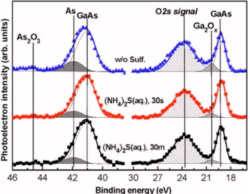
Figure1 displays As 2p3/2 and Ga 2p3/2 photoemission spectra of the as-deposited Al2O3/GaAs bilayer with and without共NH4兲2S interfacial passivation; the thickness of the overlying Al2O3thin film after 60 deposition cycles was es-timated to be approximately 63共⫾3兲 Å. Thus, we employed the high surface sensitivity of this technique共maximum
sam-pling depths of approximately 31 and 55 Å for the As 2p3/2 and Ga 2p3/2 spectra, respectively兲 to characterize the con-tent of GaAs-related chemical species diffused into the
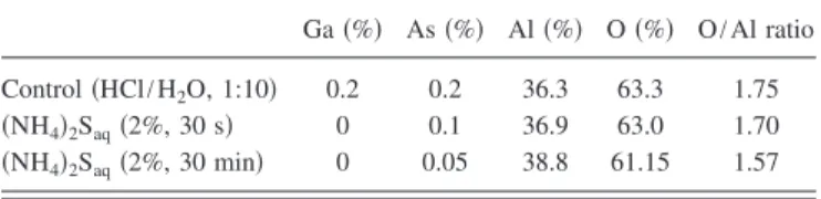
high-k layer.19In accordance to the Ga 2p3/2, As 2p3/2, Al 2p, and O 1s core levels, we evaluated the average concentration of existing GaAs oxides and the stoichiometric ratio of O to Al, based on the mixture of Ga2Oxand As2Oxin the Al2Oxbulk layer. As indicated in TableI, the concentrations of both the Ga and As oxide species were much less than 0.5%. So that, we infer that both kinds of native oxides, As2Oxand Ga2Ox, in the forms of their stoichiometric oxides and suboxides more likely formed close to oxide-substrate interface. But, we cannot rule out the possibility that a tiny amount of As oxides diffused into the Al2O3high-k film during deposition at substrate temperature up to 300 ° C. Besides, the forma-tion of these oxides, in particular, the gallium oxides, could be suppressed by forming Ga- and As-related sulfur bonds at the dielectric interface. Interestingly, it appears that the sto-ichiometry of Al2Oxin the deposited film may correlate with the degree of GaAs oxides formed nearby the interface. Pro-vided that Al2O3 was directly deposited on GaAs, the O/Al chemical ratio was as high as 1.75, i.e., an oxygen-enriched Al2Oxdielectric film; long-term sulfide immersion could re-turn this value to a nearly ideal stoichiometric ratio of 1.57 as a result of the enhanced surface stability.
The As 3d and Ga 3d core level spectra in Fig.2allowed us to characterize the interfacial composition close to the substrate because the inelastic mean free paths were above 25 Å. We found that an amorphous As layer was present on
FIG. 1. 共Color online兲 As 2p3/2and Ga 2p3/2XPS spectra of as-deposited ALD-Al2O3thin films on GaAs substrates without and with共NH4兲2S sulfide passivation.
TABLE I. Calculated relative concentrations of GaAs oxides and stoichio-metric O-to-Al ratios in as-deposited ALD-Al2O3thin films before and after chemical treatment with共NH4兲2S. Note that the As 2p3/2, Ga 2p3/2, Al 2p, and O 1s core levels were used by considering the atomic sensitivity factor. Ga共%兲 As 共%兲 Al 共%兲 O 共%兲 O/Al ratio Control共HCl/H2O, 1:10兲 0.2 0.2 36.3 63.3 1.75 共NH4兲2Saq共2%, 30 s兲 0 0.1 36.9 63.0 1.70 共NH4兲2Saq共2%, 30 min兲 0 0.05 38.8 61.15 1.57
074102-2 Cheng et al. J. Appl. Phys. 103, 074102共2008兲
the bulk GaAs; moreover, its content could be decreased upon chemical treatment with 共NH4兲2S. We suggest that these interfacial As atoms could have arisen through two mechanisms: 共a兲 the dilute HCl solution used to clean the GaAs might have led to the formation of elemental As atoms covering the GaAs surface;20 共b兲 thermal transformation of the surface As oxides might have occurred through reactions with the GaAs substrate.21 The As suboxides can desorb at approximately 150– 200 ° C, and the As2Ox species having higher oxidization states共x=3 or 5兲 will sublime at tempera-tures of approximately 250– 300 ° C.21–23This ready thermal desorption indicates that mechanism 共b兲 probably occurred during ALD deposition at 300 ° C. We also calculated the relative contributions of elemental As and the As2Ox and Ga2Oxcomponents in the respective As 3d and Ga 3d spectra 共TableII兲. Evidently, the sulfur-terminated GaAs surface suc-cessfully decreased the content of the As-rich layer and its chemical oxides.
The O 2s photoelectron signal observed at 23.4 eV, which mostly originated from the overlying Al2O3thin film, overlapped with the Ga 3d core level. The content of Ga–O oxide species existing near the Al2O3– GaAs interface de-creased after sulfidization. According to the literature,24,25the Ga–S chemical bond, relative to the As–S bond, has the higher bond strength up to 400 ° C, thereby effectively
re-straining the growth of Ga2Ox. These sulfur species are not readily identified in a S 2p spectrum because of partial over-lap with the signal of bulk Ga 3s, but a small number of GaSx bonds were detectable at a peak position of approxi-mately 162.2 eV 共not shown here兲.26 Along with the high stabilization of the Ga2O3 stoichiometric oxide, these fea-tures taken together reasonably explain the absence of the Ga–O signal in the Ga 2p3/2 spectra after surface sulfidiza-tion. In view of the improved behavior, we believe that the sulfur-terminated GaAs substrate enhanced the deposition quality and dielectric stoichiometry of the ALD-Al2O3 thin films.
Figure3displays the C-V and I-V characteristics of the various samples. The 共NH4兲2S-treated sample displayed a higher oxide capacitance accompanying a decreased C-V fre-quency dispersion, relative to those of the untreated sample; a reduction in hysteresis width and gate leakage current共Jg兲 were also achieved 关Figs. 3共b兲 and3共c兲兴. These results are indicative of the abatement of the Fermi level pinning effect in the capacitor properties; in other words, modulation of the surface potential and carrier manipulation was enhanced. As stated above, sulfide pretreatment suppressed the amounts of unstable As–As and As–O species, which are believed to be a source of high-density interfacial traps. The value of Dit close to the midgap was estimated to be approximately 1 ⫻1013cm−2eV−1 for the untreated sample; subsequent sul-fide passivation reduced this value to approximately 7 ⫻1012cm−2eV−1. Previous studies have found that sul-fidized GaAs improved the MOS characteristics as a result of eliminating As-related surface defects.27,28 The subsequent PMA at 400 ° C, however, not only caused a larger frequency dispersion and broadened hysteresis width at the depletion region but also increased the value of Jg by nearly four or-ders of magnitude. The underlying mechanisms responsible for the PMA-induced gate leakage degradation are discussed below.
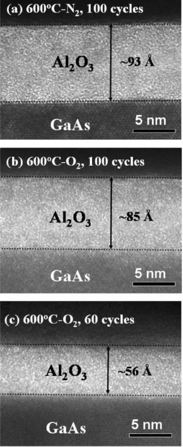
B. Effect of thermal annealing gas environment To explore the degradation of the electrical characteris-tics that were due to N2 annealing, we first compared HR-TEM images of the Pt/Al2O3 bilayers deposited on the sulfide-treated GaAs after PDA under N2 and O2 atmo-spheres 关Figs.4共a兲–4共c兲兴. We did not observe the existence of the interfacial layer; the deposited Al2O3also exhibited an amorphous phase after PDA at 600 ° C. Most importantly, the O2-processed sample revealed a bright Al2O3 thin film and an interface that was indistinct with respect to the upper Pt metal and GaAs substrate, whereas the N2-processed sample revealed a relatively dark, thick Al2O3film possess-ing a sharp interface. We believe that the O2used as the feed gas was effective in densifying the ALD-Al2O3 gate dielec-tric and repairing the inner bond imperfections, e.g., dan-gling bonds and oxygen vacancies. Meanwhile, a great de-gree of interdiffusion occurred at the dielectric-substrate interface, which can be attributed to the relatively high prob-ability of oxygen diffusing into the GaAs substrate,29 result-ing in the blurred interface for the O2-processed system.
FIG. 2. 共Color online兲 As 3d and Ga 3d XPS spectra of as-deposited ALD-Al2O3thin films on GaAs substrates with and without共NH4兲2S sulfide passivation.
TABLE II. Chemical bonding ratios of As 3d and Ga 3d core levels deter-mined by fitting the XPS data from Fig.2. Note that the contribution of the O 2s emission has been excluded.
As 3d and Ga 3d As– As/Astotal
共%兲 As2Oxa/Astotal 共%兲 Ga2Oxb/Gatotal 共%兲 Control共HCl/H2O, 1:10兲 18.5 5 17.70 共NH4兲2Saq共2%, 30 s兲 13.4 0 9.84 共NH4兲2Saq共2%, 30 min兲 12.8 0 8.86 aThe As
2Oxchemical species include As2O5, As2O3, and As suboxides. bThe Ga
2Oxchemical species include Ga2O3and Ga suboxides.
Next we examined the impact of thermal annealing on the multifrequency C-V curves, as illustrated in Figs. 5共a兲 and5共b兲; each inset displays the C-V hysteresis width mea-sured at 100 kHz. For both deposition conditions, the O2-annealed samples exhibited higher oxide capacitance and decreased hysteresis phenomena with respect to the
N2-annealed samples; we attribute this finding mainly to the highly improved dielectric quality and the thinner film thick-ness. We also found that electron trapping was responsible for the clockwise hysteresis loop,17 where the hysteresis widths after O2 and N2 PDA were approximately 0.3 and
FIG. 3.共Color online兲 共a兲 Multifrequency and 共b兲 bidirectional C-V charac-teristics and共c兲 gate leakage current 共I-V兲 curves of GaAs MOS capacitors with as-deposited Al2O3thin films after共NH4兲2S passivation and PMA at
400 ° C. FIG. 4. HRTEM images of Pt/Al2O3/sulfidized-GaAs structures with differ-ent deposition cycles and PDA conditions: 共a兲 100 cycles, N2 PDA; 共b兲 100 cycles, O2PDA;共c兲 60 cycles, O2PDA. PDA temperature: 600 ° C.
074102-4 Cheng et al. J. Appl. Phys. 103, 074102共2008兲
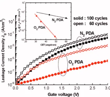
0.4 V, respectively. This situation reflected the smaller den-sity of slow traps that resided around the dielectric interface after performing O2annealing. In contrast, the I-V character-istics in Fig. 6 are remarkably different: N2 PDA severely deteriorated the Jgcharacteristics, as in the PMA case in Fig. 3共c兲, whereas the O2ambient alleviated the degradation phe-nomenon. From a plot of the value of Jg共at Vg= 2 V兲 versus the capacitance-equivalent thickness 共CET兲, the value of Jg at a CET of 40 Å was reduced by nearly three orders of magnitude after replacing N2 with O2 as the annealing gas 共inset to Fig.6兲. We ascribe the dramatically increased value of Jg to one or both of the following mechanisms: 共a兲 the elemental As overlayer that acted as a metallic contamination source nearby the oxide-bulk interface increased the surface recombination velocity, with fast diffusion resulting in poor insulator properties;共b兲 high-temperature processing caused the generation of surface pits or holes within the GaAs sub-strate, thus increasing the surface roughness.21 Excess As atoms might have been produced during either the decompo-sition of GaAs itself or the chemical transformation of oxide species through reactions with the bulk GaAs; meanwhile,
the inhomogeneous voids formed also deteriorated the sur-face morphology. We expected a relatively low density of formed voids after annealing because of the coverage of an amorphous Al2O3film on GaAs substrate. Thus, we inferred that the N2-annealed Al2O3/GaAs structures suffered from relatively severe desorption and transformation of the As2Ox and Ga2Oxmixed oxides; in addition, more As atoms were segregated at the interface. In light of this behavior, we would expect degradation of the gate leakage characteristics to be accelerated after N2annealing. To support our hypoth-esis, we performed a dielectric reliability test 共Fig.7兲 with
regard to this degradation behavior. The
Pt/ALD-Al2O3/GaAs capacitors were stressed under the constant voltage stress共Vg兲 of 5 V and a constant oxide elec-trical field共Eox兲 of 8.5 MV cm−1. Irrespective of the dielec-tric stress method employed, we found that the sulfidization procedure improved the dielectric reliability. The sulfidized sample that underwent subsequent O2 annealing possessed
FIG. 5. 共Color online兲 Multi-frequency C-V curves of sulfidized-GaAs MOS capacitors with Al2O3 thin films annealed for 共a兲 100 and 共b兲 60 deposition cycles. Each inset displays the respective C-V hysteresis mea-sured at 100 kHz.
FIG. 6. 共Color online兲 I-V Characteristics of the MOS capacitors analyzed in Fig.5. Inset: Plot of Jg共at Vg= 2 V兲 vs CET.
FIG. 7. 共Color online兲 Stress time dependence of the gate leakage Jgfor Pt/ALD-Al2O3/GaAs MOS capacitors under a constant Vgstress of 5 V共at the left y-axis兲 and a constant Eoxstress of 8.5 MV cm−1共at the right y-axis兲, respectively.
superior dielectric reliability, relative to that which under-went N2 annealing, in accordance to the slower rate of in-crease in the value of Jg. These findings indicate that the annealing environment is a crucial factor in determining the electrical performance of high-k/GaAs structures. The de-graded quality of the N2-annealed sample with respect to the O2-annealed one shall be closely linked to severe As2Ox de-sorption and the extent is not so drastic to cause the increase of the interface roughness. This is because a relatively low temperature of 600 ° C annealing was employed as compared to the previous observation reported by Passlack et al. that the Ga2O3/GaAs interface is very smooth after annealing
below 700 ° C and severely degrades with 780 ° C
annealing.16
TableIIIprovides a comprehensive list of the accessible solid state reactions involved in the Ga–As–O phase diagram30,31to aid us in determining the transformation phe-nomena that occurred during annealing. The critical tempera-ture Tc is defined as the temperature at which the reaction becomes thermodynamically favorable, i.e., where the Gibbs free energy of formation共⌬Gf兲 is less than zero; we obtained the values of Tc from experimental results reported in the literatures.21–23,34 We also calculated the value of ⌬Gf for each of these stoichiometric equations.32,33If⌬Gf is greater
than zero, the chemical reaction will not proceed; for ex-ample, the mechanisms associated with Ga2O formation are inhibited at room temperature, but an increase in temperature enhances the driving kinetics of the reaction. Because vari-ous kinds of GaAs chemical products desorb and/or trans-form during high-temperature processing, we pertrans-formed XPS and SIMS analyses to better characterize the electrical differences.
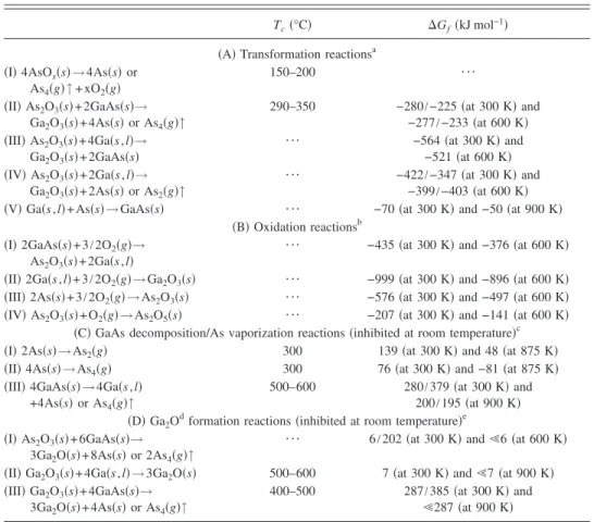
The As 2p3/2and Ga 2p3/2spectra in Fig.8indicate that the diffusion of GaAs chemical species was enhanced within the Al2O3 gate dielectric after thermal annealing; we ex-tracted the contribution of each chemical component. In the following discussion we denote the N2-annealed capacitor that underwent sulfide treatment as the “SN sample” and denote the O2-annealed capacitors without and with sulfide treatment as the “O sample” and “SO sample,” respectively. The As 2p3/2 spectra revealed an increased incorporation of arsenic oxides, including As2O5, As2O3, and AsOx, relative to their content in the as-deposited Al2O3film. We observed similar behavior in the Ga 2p3/2spectra: both the Ga2O3and GaOxoxides were slightly enriched after annealing, with the SN sample having relative higher concentrations. From the atomic quantification, TableIVindicates that the amount of diffused arsenic oxides was larger, by about one order of
TABLE III. Solid state chemical reactions of Ga–As–O associated systems. All these equations are separated into four parts.
Tc共°C兲 ⌬Gf共kJ mol−1兲 共A兲 Transformation reactionsa
共I兲 4AsOx共s兲→4As共s兲 or As4共g兲↑ +xO2共g兲 150–200 ¯ 共II兲 As2O3共s兲+2GaAs共s兲→ Ga2O3共s兲+4As共s兲 or As4共g兲↑ 290–350 −280/−225 共at 300 K兲 and −277/−233 共at 600 K兲 共III兲 As2O3共s兲+4Ga共s,l兲→ Ga2O3共s兲+2GaAs共s兲 ¯ −564共at 300 K兲 and −521共at 600 K兲 共IV兲 As2O3共s兲+2Ga共s,l兲→ Ga2O3共s兲+2As共s兲 or As2共g兲↑ ¯ −422/−347 共at 300 K兲 and −399/−403 共at 600 K兲 共V兲 Ga共s,l兲+As共s兲→GaAs共s兲 ¯ −70共at 300 K兲 and −50 共at 900 K兲
共B兲 Oxidation reactionsb 共I兲 2GaAs共s兲+3/2O2共g兲→
As2O3共s兲+2Ga共s,l兲
¯ −435共at 300 K兲 and −376 共at 600 K兲 共II兲 2Ga共s,l兲+3/2O2共g兲→Ga2O3共s兲 ¯ −999共at 300 K兲 and −896 共at 600 K兲 共III兲 2As共s兲+3/2O2共g兲→As2O3共s兲 ¯ −576共at 300 K兲 and −497 共at 600 K兲 共IV兲 As2O3共s兲+O2共g兲→As2O5共s兲 ¯ −207共at 300 K兲 and −141 共at 600 K兲
共C兲 GaAs decomposition/As vaporization reactions 共inhibited at room temperature兲c 共I兲 2As共s兲→As2共g兲 300 139共at 300 K兲 and 48 共at 875 K兲 共II兲 4As共s兲→As4共g兲 300 76共at 300 K兲 and −81 共at 875 K兲 共III兲 4GaAs共s兲→4Ga共s,l兲
+4As共s兲 or As4共g兲↑
500–600 280/379 共at 300 K兲 and 200/195 共at 900 K兲 共D兲 Ga2Odformation reactions共inhibited at room temperature兲e 共I兲 As2O3共s兲+6GaAs共s兲→
3Ga2O共s兲+8As共s兲 or 2As4共g兲↑
¯ 6/202 共at 300 K兲 and Ⰶ6 共at 600 K兲 共II兲 Ga2O3共s兲+4Ga共s,l兲→3Ga2O共s兲 500–600 7共at 300 K兲 and Ⰶ7 共at 900 K兲 共III兲 Ga2O3共s兲+4GaAs共s兲→ 3Ga2O共s兲+4As共s兲 or As4共g兲↑ 400–500 287/385 共at 300 K兲 and Ⰶ287 共at 900 K兲 aReferences22,23, and37. bReference38. cReferences23and33.
dThe standard molar Gibbs free energy of formation共⌬G
f兲 for Ga2O共s兲 was assumed to be −330 kJ mol−1, based on the standard molar enthalpy of formation共⌬Hf兲 of −356 kJ mol−1at 300 K共Ref.32兲.
eReferences23,35, and37.
074102-6 Cheng et al. J. Appl. Phys. 103, 074102共2008兲
magnitude, than that of the gallium oxides in the annealed Al2O3; this behavior is similar to that of the oxide layer formed during thermal oxidation of a GaAs surface.36In ad-dition, only the O sample after annealing at 600 ° C pre-sented an oxygen-enriched Al2Oxfilm; we attribute this find-ing to a portion of the sulfur atoms fillfind-ing a number of vacancies inside the high-k gate dielectric, thereby avoiding overoxidization in the sulfidized samples during PDA.
Table III-共A兲 indicates that the value of Tc for the de-sorption of arsenic oxides ranges from 150 to 350 ° C; these transformations are thermodynamically favorable at room
temperature. In contrast, the higher thermal stability of the Ga-based oxide compounds inhibits the reduction of non-volatile Ga2O3 into Ga2O 关Table III-共D兲兴; consequently, its value of Tc is higher 共400–600 °C兲. Because of the low sublimation point of the oxides of arsenic, volatile As2O3 oxide first reacts with either the GaAs substrate or interstitial Ga atoms to form a Ga2O3layer and segregated As close to the interface. It is possible that the highly stable Ga2O3oxide also reacts with the substrate again to produce nonstoichio-metric Ga2O along with the As coproducts under high-temperature annealing at 600 ° C. Most of these As species—in the form of elemental As and/or gaseous As4—are oxidized during the desorption event and then trapped inside the dielectric film. Note that Ga2O3formation can arise through several transformation paths; for example: As2O3+ 2GaAs→Ga2O3+ 4As or As4. Because the O2 envi-ronment provides additional reaction paths 关Table III-共B兲兴, the content of chemical products is likely to be somewhat different to that in the N2annealing case. This situation can be explained in terms of the chemical reaction principle that kinetics naturally drive several oxidation mechanisms—e.g., the oxidation of GaAs, As, and As4—resulting in a decelera-tion of the rate of transformadecelera-tion of As2Ox compounds as well as the generation of As defects in the O2ambient.38 In addition, even if molecular oxygen prefers to react with Ga atoms over As atoms, the As species will still have a higher probability of oxidation because they are more readily desorbed.39When the content of arsenic oxides increases in the upper area of the dielectric film they can act as a block, which in turn hinders the diffusion of oxygen into the dielectric-substrate region. These phenomena result in our observation of an enriched amount of As2Ox with a low Ga2Oxconcentration for both the SO and O samples, a find-ing that is opposite to the behavior of the SN sample. An-other interesting phenomenon visible in the 2p3/2 spectra is that PDA under N2resulted in the formation of some metallic As, whereas some elemental Ga appeared after PDA under O2. This finding provides direct evidence of the fast genera-tion of As species in the N2 ambient. On the other hand, as far as the source of these Ga atoms is concerned, we specu-late that the oxidation of the Al2O3/GaAs interface and de-composition of the GaAs substrate are responsible for the supply of free Ga atoms.23,38It should be pointed out that as regarding the reactions related to Al and these indiffused Ga or As oxides, most possible reaction we presume is the reac-tion of Al2O3with Ga2O3due to the higher thermal stability relative to As2O3. However, in our study the highest RTA temperature is 600 ° C, probably not enough to make Al react with Ga oxides;40these thermal processes are excluded here and still need further investigation.
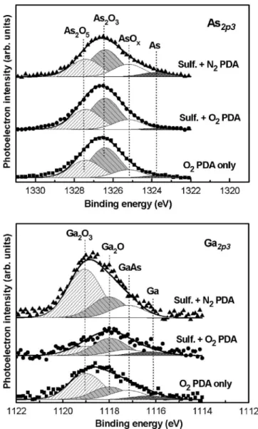
Figure9presents the highly bulk-sensitive As 3d and Ga 3d photoemissions; Table Vprovides the chemical bonding ratio of the contributed chemical components for convenient characterization. We observe that annealing at 600 ° C fur-ther decreased the percentage of interfacial As presented in the overall As 3d spectra, with respect to that in the as-deposited Al2O3/GaAs structures 共Fig. 2, Table II兲. Even though the desorption event contributed to the formation of either As or As4, most of the As atoms escaped into the
FIG. 8. As 2p3/2and Ga 2p3/2XPS spectra of 600 ° C-annealed Al2O3thin films on the sulfidized GaAs substrate. The contributing chemical compo-nents were extracted and are displayed in the respective spectra.
TABLE IV. Calculated relative concentration of GaAs oxides and stoichio-metric O-to-Al ratios in the N2- and O2-annealed ALD-Al2O3thin films with and without共NH4兲2S surface passivation.
Ga共%兲 As 共%兲 Al 共%兲 O 共%兲 O/Al ratio Sulfide+ N2600 ° C PDA 0.3 2.0 34.8 62.9 1.80 Sulfide+ O2600 ° C PDA 0.11 2.94 35.1 61.8 1.76 O2600 ° C PDA only 0.24 3.87 30.0 65.8 2.19
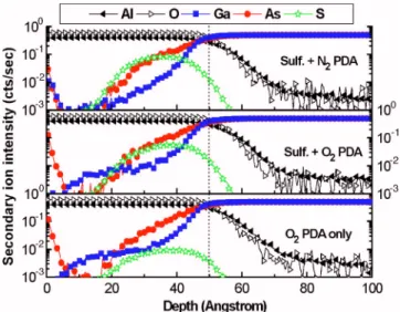
atmosphere or were further oxidized into various oxidation states. A substantial amount of Ga2Oxoxides was generated accordingly through chemical transformation. We also ob-served that the additional sulfide pretreatment of the SO sample made it共relative to the O sample兲 more highly resis-tant to the growth of these undesirable components. Figure 10 illustrates the respective SIMS depth profiles; the thick-ness of the Al2O3 thin film, which was deposited at 300 ° C for 50 cycles, was approximately 50 共⫾3兲 Å after PDA at 600 ° C. Of primary interest is the distribution of the As, Ga, and S species in the overlying Al2O3 high-k film. We found that a higher concentration of As was presented around the bottom of the Al2O3bulk film, coinciding with the diffusion of As-enriched oxides and the interfacial arsenic layer. An-other feature is the observation of a small tails of Ga species at a depth of approximately 10– 30 Å for the SO and O samples only, probably related to a trace of outdiffused Ga elements, the detailed mechanism of which requires further investigation. On the other hand, the S signal detected in the O sample was due to mass interference of molecular oxygen in the SIMS analysis of the oxide film. We believe that the S atoms did exist even after high-temperature processing, as determined after subtracting the induced signal of the mass interference used as the baseline background. The corre-sponding XPS analysis in Table IV indicates that the
sul-fidized samples were relatively less oxygen excessive共Al/O ratio= 1.78兲 with respect to the HCl-last sample 共Al/O ratio= 2.2兲. Meanwhile, the smaller C-V hysteresis width af-ter sulfidization is indicative of less charge trapping in the Al2O3 dielectric 共not shown here兲. Thus, we conclude that most of the S atoms diffused into the high-k film and prob-ably occupied either the vacancy sites or pre-existing defects; as a result, this process facilitated the improvement in the quality of the Al2O3gate dielectrics as well as their electrical performance.
IV. CONCLUSIONS
In this study, we systematically examined the interfacial characteristics and MOS properties of ALD-Al2O3dielectric films deposited on sulfidized GaAs substrates. The sulfida-tion pretreatment diminished the formasulfida-tion of GaAs native oxides and elemental As coverage close to dielectric inter-face, thus improving the effect of Fermi level pinning on the Al2O3/Ge capacitors. The sulfidized samples displayed not only smaller frequency dispersions with higher oxide capaci-tances but also decreased hysteresis widths, interfacial state densities, and gate leakages 共Jg兲. In addition, a nearly stoi-chiometric Al2O3high-k film exhibiting higher resistivity to dielectric overoxidation was obtained after performing sul-fidization. The nature of the thermal annealing environment also affected several characteristics of the systems; for ex-ample, the use of an O2ambient, relative to N2, further den-sified the Al2O3 dielectric film, alleviated charge trapping, and decreased the amount of metallic As generated, thereby improving the reliability of the value of Jg. We have clarified these phenomena in terms of identifying the underlying ther-mochemical mechanisms.
ACKNOWLEDGMENTS
This study was sponsored mainly by the National Sci-ence Council of the Republic of China under Contract No. NSC94-2215-E009-066.
FIG. 9. As 3d and Ga 3d XPS spectra of 600 ° C-annealed Al2O3thin films on the sulfidized GaAs substrate. The contributed chemical components were extracted and are displayed in the respective spectra.
TABLE V. Chemical bonding ratios of As 3d and Ga 3d core levels deter-mined by fitting the XPS data from Fig.9. Note that the contribution of the O 2s emission has been excluded.
As 3d and Ga 3d As– As/Astotal
共%兲 As2Oxa/Astotal 共%兲 Ga2Oxb/Gatotal 共%兲 Sulfide+ N2PDA at 600 ° C 10.6 20.6 17.4 Sulfide+ O2PDA at 600 ° C 6.2 26.0 16.8 O2PDA at 600 ° C only 9.2 30.8 27.6 aThe As
2Oxchemical species include As2O5, As2O3, and As suboxides. bThe Ga
2Oxchemical species include Ga2O3and Ga suboxides.
FIG. 10. 共Color online兲 SIMS depth profiles of the Al2O3/GaAs samples analyzed in Fig.9. The diffusion of As- and Ga-related chemical species into overlying high-k film was observed.
074102-8 Cheng et al. J. Appl. Phys. 103, 074102共2008兲
1S. Datta, T. Ashley, J. Brask, L. Buckle, M. Doczy, M. Emeny, D. Hayes, K. Hilton, R. Jefferies, T. Martin, T. J. Phillips, D. Wallis, P. Wilding, and R. Chau, Tech. Dig. - Int. Electron Devices Meet. 2005, 763.
2M. H. Zhang, I. J. Ok, H. S. Kim, F. Zhu, T. Lee, G. Thareja, L. Yu, and J. C. Lee,Appl. Phys. Lett.89, 042902共2006兲.
3J. Reed, Z. Fan, G. B. Gao, A. Botchkarev, and H. Morkoc,Appl. Phys. Lett.64, 2706共1994兲.
4H.-L. Lu, L. Sun, S.-J. Ding, M. Xu, D. W. Zhang, and L.-K. Wang,Appl. Phys. Lett.89, 152910共2006兲.
5C. P. Chen, Y. J. Lee, Y. C. Chang, Z. K. Yang, M. Hong, J. Kwo, H. Y. Lee, and T. S. Lay,J. Appl. Phys.100, 104502共2006兲.
6M. Zhu, C.-H. Tung, and Y.-C. Yeo,Appl. Phys. Lett.89, 202903共2006兲. 7S. Arabasz, E. Bergignat, G. Hollinger, and J. Szuber,Vacuum 80, 888
共2006兲.
8V. N. Bessolov, E. V. Konenkova, and M. V. Lebedev,J. Vac. Sci. Technol. B14, 2761共1996兲.
9Y. Dong, X. M. Ding, X. Y. Hou, Y. Li, and X. B. Li,Appl. Phys. Lett.77, 3839共2000兲.
10D. S. L. Mui, D. Biswas, J. Reed, A. L. Demirel, S. Strite, and H. Morkoc, Appl. Phys. Lett.60, 2511共1992兲.
11Z. Chen and D. Gong,J. Appl. Phys.90, 4205共2001兲.
12D. Shahrjerdi, M. M. Oye, A. L. Holmes, Jr., and S. K. Banerjee,Appl. Phys. Lett.89, 043501共2006兲.
13M. H. Zhang, I. J. Ok, H. S. Kim, F. Zhu, T. Lee, G. Thareja, L. Yu, and J. C. Lee,Appl. Phys. Lett.89, 042902共2006兲.
14A. Jaouad, V. Aimez, C. Aktik, K. Bellatreche, and A. Souifi,J. Vac. Sci. Technol. A22, 1027共2004兲.
15M.-K. Lee, C.-F. Yen, J.-J. Huang, and S.-H. Lin,J. Electrochem. Soc.
153, F266共2006兲.
16M. Passlack, J. K. Abrokwah, Z. Yu, R. Droopad, C. Overgaard, and H. Kawayoshi,Appl. Phys. Lett.82, 1691共2003兲.
17M. H. Zhang, M. Oye, B. Cobb, F. Zhu, H. S. Kim, I. J. Ok, J. Hurst, S. Lewis, A. Holmes, J. C. Lee, S. Koveshnikov, W. Tsai, M. Yakimov, V. Torkanov, and S. Oktyabrsky,J. Appl. Phys.101, 034103共2007兲.
18W. A. Hill and C. C. Coleman,Solid-State Electron.23, 987共1980兲. 19NIST Electron Inelastic-Mean-Free-Path Database 71 共v. 1.1兲, National
Institute of Standards and Technology, 2000.
20K. W. Frese and S. R. Morrison,Appl. Surf. Sci.8, 266共1981兲.
21A. G. Cervantes, Z. R. Alvarez, M. L. Lopez, E. L. Luna, and I. H. Calderon,Thin Solid Films373, 159共2000兲.
22J. P. Contour, J. Massies, H. Fronius, and K. Ploog,Jpn. J. Appl. Phys., Part 227, L167共1988兲.
23M. Yamada and Y. Ide,Surf. Sci.339, L914共1995兲.
24H. Sugahara, M. Oshima, H. Oigawa, H. Shigekawa, and Y. Nannichi,J. Appl. Phys.69, 4349共1991兲.
25H. Sik, Y. Feurprier, C. Cardinaud, G. Turban, and A. Scavennec,J. Elec-trochem. Soc.144, 2106共1997兲.
26M. V. Lebedev, T. Mayer, and W. Jaegermann,Surf. Sci.547, 171共2003兲. 27J.-K. Yang, M.-G. Kang, and H.-H. Park,J. Appl. Phys.96, 4811共2004兲. 28L. J. Huang, W. M. Lau, S. Ingrey, D. Landheer, and J.-P. Noel,J. Appl.
Phys.76, 8192共1994兲.
29B. R. Chakraborty, N. Dilawar, S. Pal, and D. N. Bose, Thin Solid Films
411, 240共2002兲.
30Yu. V. Medvedev,Appl. Phys. Lett.64, 3458共1994兲.
31C. D. Thurmond, G. P. Schwartz, G. W. Kammlott, and B. Schwartz,J. Electrochem. Soc.127, 1366共2006兲.
32D. R. Lide, CRC Handbook of Chemistry and Physics: a Ready-Reference Book of Chemical and Physical Data, 84th ed.共CRC, Boca Raton, FL, 2003兲.
33O. Knacke, O. Kubaschewski, and K. Hesselmann, Thermochemical Prop-erties of Inorganic Substances共Springer, Berlin, 1991兲.
34K. Tone, M. Yamada, Y. Ide, and Y. Katayama,Jpn. J. Appl. Phys., Part 2
31, L721共1992兲.
35G. W. Smith, A. J. Pidduck, C. R. Whitehouse, J. L. Glasper, and A. M. Keir,Appl. Phys. Lett.64, 3458共1994兲.
36S. C. Ghosh, M. C. Biesinger, R. R. LaPierre, and P. Kruse,J. Appl. Phys.
101, 114322共2007兲.
37S. C. Ghosh, M. C. Biesinger, R. R. LaPierre, and P. Kruse,J. Appl. Phys.
101, 114321共2007兲.
38D. A. Allwood, S. Cox, N. J. Mason, R. Palmer, R. Young, and P. J. Walker,Thin Solid Films412, 76共2002兲.
39J. S. Song, Y. C. Choi, S. H. Seo, D. C. Oh, M. W. Cho, T. Yao, and M. H. Oh,J. Cryst. Growth264, 98共2004兲.
40M. Takahashi, T. Nakatani, S. Iwamoto, T. Watanabe, and M. Inoue, J. Phys.: Condens. Matter 18, 5745共2006兲.