Oxide-Relief and Zn-Diffusion 850-nm
Vertical-Cavity Surface-Emitting Lasers With
Extremely Low Energy-to-Data-Rate
Ratios for 40 Gbit/s Operations
Jin-Wei Shi, Senior Member, IEEE, Jhih-Cheng Yan, Jhih-Min Wun, Jason Chen, and Ying-Jay Yang
Abstract—We demonstrate novel structures of a vertical-cavity surface-emitting laser (VCSEL) for high-speed (∼40 Gbit/s) oper-ation with ultralow power consumption performance. Downscal-ing the size of oxide aperture of VCSELs is one of the most ef-fective ways to reduce the power consumption during high-speed operation. However, such miniaturized oxide apertures (∼2 μm diameter) in VCSELs will result in a large differential resis-tance, optical single-mode output, and a small maximum output power (< 1 mW). These characteristics seriously limit the max-imum electrical-to-optical (E–O) bandwidth and device reliabil-ity. By the use of the oxide-relief and Zn-diffusion techniques in our demonstrated 850-nm VCSELs, we can not only release the burden imposed on downscaling the current-confined aperture for high speed with low-power consumption performance, but can also manipulate the number of optical modes inside the cavity to max-imize the E–O bandwidth and product of bit-rate transmission distance in an OM4 fiber. State-of-the-art dynamic performances at both room temperature and 85◦C operations can be achieved by the use of our device. These include extremely high D-factors (∼13.5 GHz/mA1 /2), as well as record-low energy-to-data ratios
(EDR: 140 fJ/bit) at 34 Gbit/s operation, and error-free transmis-sion over a 0.8-km OM4 multimode fiber with a record-low energy-to-data distance ratio (EDDR: 175.5 fJ/bit.km) at 25 Gbit/s.
Index Terms—Semiconductor lasers, vertical-cavity surface-emitting lasers (VCSELs).
I. INTRODUCTION
H
IGH-SPEED, high-efficiency, and low power consump-tion vertical-cavity surface-emitting lasers (VCSELs) that operate at a wavelength of 850 nm or around 1000 nm have lately attracted a lot of attention due to their suitability for appli-cations in optical interconnects (OI) [1]–[12]. Compared withManuscript received May 11, 2012; revised June 23, 2012; accepted July 24, 2012. Date of publication July 31, 2012; date of current version April 3, 2013. This work was supported by the Ministry of Economic Affairs of Taiwan under Grant 98-EC-17-A-07-S1-001.
J.-W. Shi, J.-C. Yan, and J.-M. Wun are with the Department of Electrical En-gineering, National Central University, Taoyuan 320, Taiwan (e-mail: jwshi@ ee.ncu.edu.tw; [email protected]; [email protected]).
J. Chen is with the Department of Photonics, National Chiao-Tung Univer-sity, Hsinchu 300, Taiwan (e-mail: [email protected]).
Y.-J. Yang is with the Department of Electrical Engineering, National Taiwan University, Taipei 106, Taiwan (e-mail: [email protected]).
Color versions of one or more of the figures in this paper are available online at http://ieeexplore.ieee.org.
Digital Object Identifier 10.1109/JSTQE.2012.2210863
the reported edge-emitting distributed feed-back (DFB) laser with its state-of-the-art dynamic performance at a wavelength of 1.3 μm [13]–[15] which is used for an OI application, the power consumption of 850 or∼1000 nm VCSELs for >25 Gbit/s oper-ation is less than 1/10 [16]. There are two important parameters necessary for evaluating power consumption during high-speed operation of VCSELs.
One is the modulation current efficiency (D-factor) and the other is the threshold current Ith [1]–[12]. In order to further reduce the required power consumption Ith and increase the D-factor of VCSELs, there are two major trends under de-velopment. The one involves using the highly strain multiple quantum wells (MQWs) to increase the differential gain in the active layers and improve the D-factor performance [5], [6], [8], [10]–[12], [17]. Another approach is to greatly downscale the size of the oxide aperture to reduce Ith [3], [4]. Recently, by downscaling the diameter of the oxide aperture to around 2 μm, record-low energy-to-data ratio (EDR: 83 fJ/bit) of 850-nm single-mode VCESLs with excellent transmission perfor-mance under 17 Gbit/s and at room temperature (RT) opera-tion has been demonstrated [3]. However, compared with the reported high-performance 850-nm VCSEL with a larger ox-ide aperture (∼6 μm), a significant degradation in the maxi-mum 3-dB electrical-to-optical (E–O) bandwidth is observed (23 Gbit/s [2] versus ∼13 Gbit/s [3]). Such degradation in speed performance might be attributable to the tremendous in-crease in the differential resistance of a VCSEL (∼570 Ω [3]) with such a small oxide aperture (∼2 μm), the single-mode output-induced spatial hole burning effect [18]–[20], and the relaxation oscillation (RO) frequency-limited E–O bandwidth [19]–[21]. In addition, the significant stress of (double) oxide layers [1], [2], [8] on the active regions should be regarded as a more serious issue impacting the reliability of these VCSELs when their current-confined oxide apertures [22] are further downscaled. In this paper, we demonstrate a novel high-speed VCSEL that operates at the 850-nm wavelength, incorporat-ing oxide-relief [12] and Zn-diffusion [11], [19]–[21] struc-tures to overcome the aforementioned limitations of VCSELs with miniaturized oxide apertures. By selective removing the single-oxide layer in our VCSEL structure, the reduction in the parasitic capacitance, the improvements in the D-factor, and maximum modulation speed have been demonstrated [12]. Fur-thermore, in order to further reduce the device resistance, ma-nipulate the number of optical modes inside the VCSEL cavity,
Fig. 1. (a) Conceptual cross-sectional view of devices A and B, and (b) top view of the demonstrated device.
and maximize both the E–O bandwidth and product of bit-rate transmission distance in the OM4 fiber, the Zn-diffusion tech-niques are applied to the top DBR mirror. The VCSEL with an ∼4-μm diameter current-confined (oxide) aperture and opti-mized Zn-diffusion depth demonstrates state-of-the-art perfor-mance. It includes extremely large D-factor (13.2 GHz/mA1/2), record-low energy-to-data ratios (EDR: 140 fJ/bit) at 34 Gbit/s operation [1]–[12], and 25 Gbit/s error-free transmission over a 0.8-km OM4 multi-mode fiber with a record-low energy-to-data distance ratio (EDDR: 175.5 fJ/bit.km) [23], [24].
II. DEVICESTRUCTURE ANDFABRICATION
Fig. 1(a) and (b) shows the conceptual cross-sectional and top views of the demonstrated device, respectively. As can be seen in Fig. 1(b), the fabricated device has a 26-μm diameter ac-tive mesa, which is integrated with co-planar waveguide (CPW) pads for on-wafer high-speed measurement. The epilayer struc-ture grown on a semi-insulating GaAs substrate is composed of three In0.15Al0.1Ga0.75As/Al0.3Ga0.7As MQWs sandwiched between 30-pair n-type and 20-pair p-type Al0.9Ga0.1As/ Al0.12Ga0.88As distributed-Bragg-reflector (DBR) layers with an Al0.98Ga0.02As layer above the MQWs for oxidation [11]. Compared with that reported for In0.1Ga0.9As/Al0.37Ga0.63As strained 850-nm VCSELs [17], we can achieve a higher in-dium mole fraction (0.15 versus 0.1) with a thicker well width (50 ˚A versus 40 ˚A) due to the incorporation of Al, which en-larges the bandgap but has no significant influence on the lat-tice constant (strain) of the well layer. This means that our strained VCSEL structure has a higher indium mole fraction and a wider well width than those of InGaAs-based strained 850-nm VCSELs [17] which may lead to a more significant improvement in static/dynamic performance and uniformity of wafer, respectively. An oxidation technique is used to define a circular current-confined area 4 μm in diameter. Here, the single-oxide layer is adopted in our structure simply to realize the oxide-relief structure. By the use of a chemical solution, which offers excellent etching selectivity between the AlxO1−x
layer and active (Al(In)GaAs) layers, we can thus get a very high yield (>90%) with the fabricated device. Due to the fact that the dielectric constant of air is just around one-half that of the AlxO1−x layer, there is a further reduction in the parasitic
capacitance, as confirmed by microwave scattering (S) parame-ter measurement and device modeling techniques carried out on the oxide-relief and control VCSELs. The measurement results clearly indicate that the oxide-relief structure can effectively reduce the parasitic capacitance of the VCSEL. Details about the device modeling process for our VCSELs can be referred to our previous works [20]. Fig. 1(a) shows the Zn-diffusion structure with two different geometric sizes (devices A and B) realized in the top DBR of our oxide-relief VCSEL, which can further reduce the device resistance due to the disordering of the DBR structure after Zn-diffusion [11], [19]–[21]. Furthermore, we can also control the depth of Zn-diffusion to manipulate the number of optical modes inside our cavity [20], which has a significant influence on the transmission experiment as will be discussed later.
The diameter and depth of the Zn-diffusion aperture in device A is 6 μm and∼1 μm, respectively. The 6-μm Zn-diffusion aper-ture with a >1.5 μm diffusion depth will ensure stable single-mode output performance in 850-nm VCSELs [11], [19], [20]. During high-speed data transmission, the single-mode output might reduce the mode dispersion in the fiber and benefit the product of bit-rate transmission distance [23], [24]. However, the pure single-mode performance in the VCSEL usually in-duces a serious spatial hole burning effect, which will result in a serious low-frequency roll-off and limit the maximum E–O bandwidth of the VCSEL [19]–[21]. In device A, we thus adopt a Zn-diffusion depth of less than 1 μm, to avoid the pure single-mode performance and balance the tradeoff between the maximum modulation speed and fiber transmission distance. On the other hand, in order to further reduce the differential resis-tance of the VCSEL and improve the RC-limited bandwidth, a larger Zn-diffusion depth (time) is desired. In order to avoid the pure single-mode output performance, in device B, we adopt a Zn-diffusion aperture with a depth of 1.5 μm but a diame-ter larger than 6 μm (∼10 μm). We can thus expect a smaller differential resistance for device B than device A.
III. MEASUREMENTRESULTS
Fig. 2 shows the light output versus current (L–I) and the bias current versus voltage (I–V) characteristics of devices A and B. As can be seen, both devices exhibit the same low threshold current (∼0.4 mA). Such a result clearly indicates that our Zn-diffusion process does not seriously degrade the threshold current performance [11], [19], [20]. Furthermore, we can clearly see that device B has a lower differential resistance than that of device A due to its larger Zn-diffusion depth, as ex-pected. This result leads to an improvement in the output power and differential quantum efficiency under a high bias current (I >∼4 mA). Overall, the differential resistance achieved by these two devices (A and B) can be as low as∼140 Ω (under 6 mA bias current). Such a value is smaller than the values
Fig. 2. Characteristics of the optical output power L and voltage V versus biasing current I of devices A and B.
Fig. 3. Measured optical spectra of device A under different bias currents.
typically reported for high-speed VCSELs for >25 Gbit/s oper-ation (>200 Ω) [1]–[5], [8].
During dc measurement, we have tested over 30 VCSELs each for device structures A and B, which were fabricated on two different chips. The number of total devices per chip was around 100.
Around 80% of the L–I and I–V curves measured for these devices exhibit similar characteristics and trends to those illus-trated in Fig. 2. This evidence clearly indicates the uniformity and repeatability of the Zn-diffusion and oxide-relief processes, which also supports our conclusion regarding the device mea-surement results, as will be discussed later. Figs. 3 and 4 show the optical spectra for devices A and B measured under different bias currents. As can be seen, under a very small bias current (I < 0.6 mA), both devices exhibit (near) single-mode behavior. On the other hand, when the bias current is further increased, both devices exhibit multimode performance, with device B having a larger number of optical modes due to its larger diameter of Zn-diffusion aperture (10 μm versus 6 μm). The different num-ber of optical modes between these two devices would have a determinant influence on their performance in 25 Gbit/s data transmission, as will be discussed later in Figs. 14 and 15.
The high-speed E–O performance of the fabricated devices was measured by a lightwave component analyzer (LCA), which was composed of a network analyzer (Anritsu 37397 C) and a calibrated 25-GHz photoreceiver module (New focus 1481-S).
Fig. 4. Measured optical spectra of device B under different bias currents.
Fig. 5. Measured E–O frequency responses of device A under different bias currents and RT operation.
Fig. 6. Measured E–O frequency responses of device B under different bias currents and RT operation.
Figs. 5 and 6 show the E–O responses of devices A and B, re-spectively, under different bias currents at RT. As can be seen, both these two devices can achieve∼21 GHz 3-dB bandwidth with bias currents as low as∼3 mA. Such a value is just around one-half of the required bias current reported for a 40 Gbit/s 850-nm VCSEL with a similar O-E bandwidth performance (∼22 GHz at 8 mA) [1], [2]. In addition, the maximum 3-dB E–O bandwidth of device B is slightly higher than that of device A (22 GHz versus 21 GHz). This can be attributed to the lower differential resistance of device B, as shown in Fig. 1, and a higher RC-limited bandwidth can thus be expected. Fig. 7(a) and (b) shows the relaxation oscillation (RO) frequency (fR)
(based on the shown E–O response in Fig. 4) versus√I− Ith of these two devices, where I is the bias current and Ith is the
Fig. 7. Measured fR versus (I− It h)1 / 2 and extracted D-factors of (a) device A and (b) device B.
threshold current. The slope D of these fitting lines can be used to evaluate how fast fRincreases with the bias current. A slightly
larger D-factor is extracted for device B than that for device A. Its value can be as large as 13.4 GHz/mA1/2, which is even higher than that of the reported high-performance 850-nm VC-SELs [3] which have a smaller diameter of oxide aperture (4 μm versus 2 μm). However, our measurement result here is some-what in conflict with that obtained in previous work [19], [20], which stated that the VCSEL with a (near) single-mode (smaller number of optical modes) performance would have a larger D-factor than that of the highly multimode VCSEL, due to the minimization of the spreading of injected carriers into different optical modes during operation. This contradiction can be ex-plained as follows. As reported in our previous work [20], the near single-mode VCSEL has a significant larger D-factor than that of the multi-mode control only under a small bias current regime (< 2 mA). When the bias current is further increased, the E–O bandwidth of the single-mode VCSEL becomes saturated and limited by fR[21], but the bandwidth of the multimode
VC-SEL can still increase with the increase in the bias current [20] until eventually exhibiting a much larger maximum 3-dB band-width (17 GHz versus 12.5 GHz) than that of the single-mode device. This would result in a larger D-factor for the multimode device under the high bias regime. This nonlinear relation be-tween the bias current and E–O bandwidth suggests that we may not precisely predict the large-signal (large current swing) modulation characteristics of VCSELs just by the use of the extracted single D-factor value.
Although device A has a smaller number of optical modes and higher carrier injection efficiency than device B, its near single-mode characteristic demonstrates a more serious fR-limited
3-dB bandwidth and degradation in the maximum 3-dB E–O bandwidth as well as the values of the D-factor. We thus mea-sure a slightly larger D-factor for device B than for device A.
Figs. 8–11 show the measured−log [bit error rate (BER)] versus Vppof these two devices under different data rates (12.5, 25,∼40 Gbit/s) and different bias currents operations at RT. Their insets show the corresponding error-free eye patterns un-der the operation conditions with the lowest bias current (power consumption).
For eye-pattern measurement, we adopted a 25-GHz photore-ceiver module (New focus 1481-S) connected with a wideband (100 kHz to 65 GHz) radio-frequency (RF) amplifier
(Centel-Fig. 8. Measured values of−log (BER) at 12.5 Gbit/s versus RF peak-to-peak driving voltage (Vp p) of (a) device A and (b) device B under different bias currents.
Fig. 9. Measured values of−log (BER) at 25 Gbit/s versus RF peak-to-peak driving voltage (Vp p) of (a) device A and (b) device B under different bias currents.
Fig. 10. Measured values of−log (BER) at around 35 Gbit/s versus RF peak-to-peak driving voltage (Vp p) of (a) device A and (b) device B under different bias currents.
Fig. 11. Measured values of−log (BER) at 40 Gbit/s versus RF peak-to-peak driving voltage (Vp p) of device B under different bias currents.
lax, UA0L65VM) to serve as our 40 Gbit/s receiver. Here, we use three parameters—energy-to-data rate (EDR) ratio (fJ/bit),
heat-to-bit rate (HBR) ratio (mW/Tbs), and energy-to-data dis-tance (EDDR) ratio (fJ/(bit·km)) [23], [24]—to evaluate the eye-pattern performance of our devices. For a detailed defini-tion of these three parameters, refer to [23]. A duplicate of these three definitions follows
EDR = Pe BR (1) HBR =Pdiss BR (2) EDR = Pe (BR× d) (3)
where Pe= V×I is the total consumed dc electrical power, V and I are the VCSEL’s bias voltage and current during high-speed
modulation, respectively, Pdiss= Pe−Popticalis the dissipated power, Poptical is the output optical power, BR is the bit rate, and d is the transmission distance in the optical fiber.
As can be seen, there is a significant increase in the values of BER for both devices with the driving voltage under the low-bias current regime (∼1 mA), as shown in Figs. 8 and 9. This phenomenon mainly arises because, under such a low-bias current, which is near the threshold current, the operation point of the device is close to the highly nonlinear regime of the L–I curve. The larger driving voltage (current swing) leads to more serious distortion of the eye patterns and increases the BER values. On the other hand, when there is a further increase in the bias current, the operation point is closer to the linear regime (center) of the L–I curve. The influence of the magnitude of the driving voltage on the waveform quality of the eye pattern and the BER values can thus be minimized.
Furthermore, compared with that of device A, due to the smaller differential resistance and higher maximum E–O band-width, device B can achieve a higher maximum error-free data rate (37 Gbit/s versus 34 Gbit/s), as shown in Fig. 10(a) and (b). Nevertheless, device A exhibits smaller values of EDR and HBR compared with those of device B. Under RT operation, device A can achieve error-free 34 Gbit/s eye pattern under a bias current as low as 2.3 mA with an extremely small 0.55 V peak-to-peak driving voltage (Vpp).
The superior power consumption performance of device A compared to device B can mainly be attributed to the smaller number of optical modes inside the VCSEL cavity of device A, which would minimize the spreading of injected carriers into different optical modes, enhance the large-signal modulation efficiency, and possibly minimize the mode-selective loss, which would lead to degradation in the quality of the measured eye pattern [18], [20], [25]. Although device B has a slightly larger D-factor (modulation current efficiency) compared with device A, it cannot be used to accurately evaluate the large-signal eye-pattern performance of both devices, as discussed in Fig. 7.
In addition, as shown in Fig. 11, by further boosting the bias current of device B up to 4.4 mA, a near error-free 40 Gbit/s op-eration can be achieved. Such 40 Gbit/s BER values are limited by the intersymbol interference (ISI) noise from our VCSEL. When the injected data rate reaches 40 Gbit/s, there is a slight degradation in the measured signal-to-noise ratio of the eye
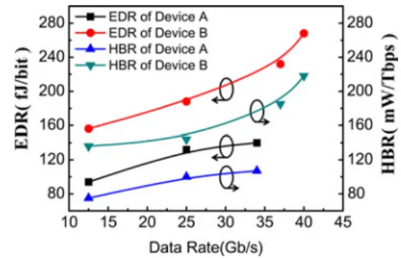
pat-Fig. 12. Measured values of EDR and HBR of devices A and B versus different data rates
tern due to the limited E–O bandwidth of device B. As can be seen, the maximum bandwidth of device B is around 22.4 GHz, which is marginal for 40 Gbit/s error-free operations [1]. It should be possible to further push our 40 Gbit/s BER values to the error-free regime (BER <1 × 10⁻¹²) by using a pho-toreceiver module with an improved sensitivity at 40 Gbit/s. At the receiver end, as adopted here, there is no transimpedance amplifier (TIA) integrated with our photodiode for 40 Gbit/s eye-pattern measurement (New focus 1481-S).
Fig. 12 shows all detailed values of EDR and HBR for these two devices under different data rates of operation. We can clearly see that the required values of EDR and HBR gradually increase with the data rate and record low values are achieved (EDR:140 fJ/bit, HBR: 107 mW/Tbs) at 34 Gbit/s by device A among all the reported high-speed VCSELs with an operation speed close to 40 Gbit/s [1], [2], [4]–[6], [8]. Table I shows the benchmark for the reported high-speed VCSELs with their maximum data rate, EDR, and HBR. Our achieved values of EDR/HBR are close to the results reported in [3] but at a signif-icant higher data rate (34 Gbit/s versus 25 Gbit/s).
High-speed VCSEL performance under 85◦C operation is also an important issue for practical applications of VCSELs with miniaturized sizes of oxide aperture [3], [24]. Fig. 13(a) and (b) shows the measured error-free eye diagram for devices A and B at their maximum modulation speed under 85◦C eration. Compared with the measurement results under RT op-eration, we can clearly observe that the required bias current increases slightly (2.3 to 2.9 mA for device A) and the maxi-mum modulation speed degrades from 34 (37) to 32 (34) Gbit/s for device A (B).
The high-speed performance under high-temperature opera-tion of our device is superior to that reported for multioxide 850-nm VCSELs with a miniaturized oxide aperture of around ∼2 μm [3], [24]. This is because the Zn-diffusion technique allows the differential resistance of the VCSEL to be signifi-cantly reduced, which implies less device heating under high-temperature operation.
Due to the increase in the area of modern data centers, it is important to increase the maximum transmission distance to around 1 km of OI [23], [24]. However, the bandwidth–distance product of standard OM4 multimode fibers is limited to around 4.5 GHz·km transmission distance [26]. Figs. 14 and 15 show the −log (BER) measured at 25 Gbit/s operation versus the
TABLE I
BENCHMARK FORHIGH-SPEED ANDGREENVCSELS
Fig. 13. Measured eye patterns and corresponding operation conditions at 85◦C of (a) device A and (b) device B at their maximum operation speed.
optical power (receiver end) and injected bias current (transmit-ter side) of devices A and B, respectively. The multimode fiber we adopted is the standard OM4 fiber. As can be seen, device A exhibits a much longer error-free transmission distance (0.8 km versus 0.1 km) than device B at the same data rate (25 Gbit/s). The EDDR achieved by device A is as low as 175.5 fJ/bit·km. To the best of the authors’ knowledge, this number is the record reported for all VCSELs [24] for 25 Gbit/s data transmission through multimode fibers. The superior transmission perfor-mance of device A compared to device B can be attributed to the fact that device A has a smaller number of optical modes, which minimize the serious mode dispersion in the multimode fiber for high-speed data transmission [23], [24]. In addition, as shown in Fig. 14, device A exhibits a distinct behavior in the measured trace of−log (BER) versus bias current. As can be seen, there is a wide bias current range (1.8–2.7 mA) for error-free transmission performance and a further increase in the bias current (>2.7 mA) would lead to degradation in the BER performance. This result can be attributed to the fact that the increase in bias current induces a more significant multi-mode phenomenon in the optical spectra, as shown in Figs. 3 and 4, which can seriously degrade transmission performance due to the mode dispersion. Such a result clearly indicates that the output optical spectra of high-speed VCSELs play an im-portant role in 25 Gbit/s transmissions through OM4 multimode fibers. In addition, in order to investigate the 25 Gbit/s transmis-sion performance at 85◦C, we also measure the optical spectra of device A when the ambient temperature rises to 85◦C. The optical spectra measured at RT and 85◦C are very similar in terms of number of modes and side-mode suppression ratio (SMSR), except for the red-shift at the center wavelength. Both measurement results, for the optical spectra and dynamic speed performance at high temperature, as shown in Fig. 13, confirm
Fig. 14. Measured−log (BER) at 25 Gbit/s through 0.8-km OM4 fiber trans-mission versus received optical power and injected bias current of device A.
Fig. 15. Measured−log (BER) at 25 Gbit/s through 0.1-km OM4 fiber trans-mission versus received optical power and injected bias current of device B.
the feasibility of using device A for 25 Gbit/s data transmission at 85◦C.
IV. CONCLUSION
In conclusion, we demonstrate a novel VCSEL structure for high-speed, ultralow power consumption, and short-reach (∼1 km) data transmission through standard OM4 multimode fibers. By using the Zn-diffusion and oxide-relief structures in our demonstrated VCSEL, we can greatly reduce the large differential resistance of VCSELs with a miniaturized oxide aperture, further enhance the RC-limited bandwidth of the
device, and manipulate the optical mode inside cavity to im-prove the transmission performance. State-of-the-art dynamic performances, which include record-low EDR: 140 fJ/bit at data rate as high as 34 Gbit/s and record-low EDDR: 175.5 fJ/bit.km at 25 Gbit/s transmission over a standard OM4 fiber, can be achieved by the use of our demonstrated device with optimized sizes of Zn-diffusion and oxide-relief aperture.
ACKNOWLEDGMENT
The authors would like to thank Dr. C.-H. Lin in Larry Col-dren’s group at the University of California Santa Barbara for valuable technical discussions about VCSEL processing. The authors also want to thank A. Joel in IQE Europe Ltd. for his support in epitaxial layers growth.
REFERENCES
[1] P. Westbergh, J. S. Gustavsson, B. Kogel, A Haglund, A. Larsson, A. Mutig, A. Nadtochiy, D. Bimberg, and A. Joel, “40 Gbit/sec error-free operation of oxide-confined VCSEL,” Electron. Lett., vol. 46, no. 14, pp. 1014–1016, Jul. 2010.
[2] A. Larsson, P. Westbergh, J. Gustavsson, A. Haglund, and B. Kogel, “High-speed VCSELs for short reach communication,” Semicond. Sci. Technol., vol. 26, p. 014017, Nov. 2010.
[3] P. Moser, W. Hofmann, P. Wolf, J. A. Lott, G. Larisch, A. Payusov, N. N. Ledentsov, and D. Bimberg, “81 fJ/bit energy-to-data ratio of 850 nm vertical-cavity surface-emitting lasers for optical interconnects,” Appl. Phys. Lett., vol. 98, no. 23, p. 231106, Jun. 2011.
[4] P. Moser, P. Wolf, A. Mutig, G. Larisch, W. Unrau, W. Hofmann, and D. Bimberg, “85◦C error-free operation at 38 Gb/s of oxide-confined 980-nm vertical-cavity surface-emitting lasers,” Appl. Phys. Lett., vol. 100, no. 8, p. 081103, Feb. 2012.
[5] K. Yashiki, N. Suzuki, K. Fukatsu, T. Anan, H. Hatakeyama, and M. Tsuji, “1.1-μm-range high-speed tunnel junction vertical-cavity surface-emitting lasers,” IEEE Photon. Technol. Lett., vol. 19, no. 23, pp. 1883–1885, Dec. 2007.
[6] H. Hatakeyama, T. Anan, T. Akagawa, K. Fukatsu, N. Suzuki, K. Toku-tome, and M. Tsuji, “Highly reliable high-speed 1.1-μm-range VCSELs with InGaAs/GaAsP-MQWs,” IEEE J. Quantum Electron., vol. 46, no. 6, pp. 890–897, Jun. 2010.
[7] C.-K. Lin, A. Tandon, K. Djordjev, S. W. Corzine, and M. R. T. Tan, “High-Speed 985 nm bottom-emitting VCSEL arrays for chip-to-chip parallel optical interconnects,” IEEE J. Sel. Topics Quantum Electron., vol. 13, no. 5, pp. 1332–1339, Sep./Oct. 2007.
[8] Y.-C. Chang, C. S. Wang, and L. A. Coldren, “High-efficiency, high-speed VCSELs with 35 Gbit/s error-free operation,” Electron. Lett., vol. 43, no. 19, pp. 1022–1023, Sep. 2007.
[9] C.-H. Lin, Y. Zheng, M. Gross, M. J. W. Rodwell, and L. A. Coldren, “High-speed potential of field-induced charge-separation lasers for short-link applications,” in Proc. Optical Fiber Commun. Conf., Los Angeles, CA, Mar.2010, Paper OWD5.
[10] S. Imai, K. Takaki, S. Kamiya, H. Shimizu, J. Yoshida, Y. Kawakita, T. Tak-agi, K. Hiraiwa, H. Shimizu, T. Suzuki, N. Iwai, T. Ishikawa, N. Tsukiji, and A. Kasukawa, “Recorded low power dissipation in highly reliable 1060-nm VCSELs for “Green” optical interconnection,” IEEE J. Sel. Topics Quantum Electron., vol. 17, no. 6, pp. 1614–1619, Nov./Dec. 2011. [11] J.-W. Shi, W.-C. Weng, F.-M. Kuo, Y.-J. Yang, S. Pinches, M. Geen, and A. Joel, “High-performance Zn-Diffusion 850-nm vertical-cavity surface-emitting lasers with strained InAlGaAs multiple quantum wells,” IEEE Photon. J., vol. 2, no. 6, pp. 960–966, Dec. 2010.
[12] J.-W. Shi, W.-C. Weng, F.-M. Kuo, J.-I. Chyi, S. Pinches, M. Geen, and A. Joel, “Oxide-relief vertical-cavity surface-emitting lasers with ex-tremely high data-rate/power-dissipation ratios,” in Proc. Optical Fiber Commun. Conf. 2011, Los Angeles, CA, Mar. 2011, Paper OThG2. [13] W. Kobayashi, T. Tadokoro, T. Fujisawa, N. Fujiwara, T. Yamanaka, and
F. Kano, “40-Gbps direct modulation of 1.3-μm InGaAlAs DFB laser in compact To-CAN package,” in Proc. Optical Fiber Commun. Conf. 2011, Los Angeles, CA, Mar. 2011, Paper OWD2.
[14] T. Simoyama, M. Matsuda, S. Okumura, A. Uetake, M. Ekawa, and T. Ya-mamoto, “40-Gbps transmission using direct modulation of 1.3-μm Al-GaInAs MQW distributed-reflector lasers up to 70◦C,” in Proc. Optical Fiber Commun. Conf. 2011, Los Angeles, CA, Mar. 2011, Paper OWD3.
[15] K. Adachi, K. Shinoda, T. Kitatani, D. Kawamura, T. Sugawara, and S. Tsuji, “Uncooled 25-Gb/s operation of a four-wavelength 1.3-μm surface-emitting DFB laser array,” in Proc. IEEE Photonic Soc. Meet-ing, Arlington, VA, Oct. 2011, Paper TuD3.
[16] D. Bimberg, “Green data and computer communication,” in Proc. IEEE Photonic Soc. Meeting, Arlington, VA, Oct. 2011, Paper TuN3. [17] S. B. Healy, E. P. O’Reilly, J. S. Gustavsson, P. Westbergh, A. Haglund,
A. Larsson, and A. Joel, “Active region design for high-speed 850-nm VCSELs,” IEEE J. Quantum Electron., vol. 46, no. 4, pp. 506–512, Apr. 2010.
[18] J. S. Gustavsson, ˚A. Haglund, J. Bengtsson, P. Modh, and A. Larsson, “Dy-namic behavior of fundamental-mode stabilized VCSELs using shallow surface relief,” IEEE J. Quantum Electron., vol. 40, no. 6, pp. 607–619, Jun. 2004.
[19] J.-W. Shi, C.-C. Chen, Y.-S. Wu, S.-H. Guol, and Y.-J. Yang, “High-power and high-speed Zn-diffusion single fundamental-mode vertical-cavity surface-emitting lasers at 850 nm wavelength,” IEEE Photon. Technol. Lett., vol. 20, no. 13, pp. 1121–1123, Jul. 2008.
[20] J.-W. Shi, C.-C. Chen, Y.-S. Wu, S.-H. Guol, and Y.-J. Yang, “The influ-ence of diffusion depth on the static and dynamic behaviors of Zn-diffusion high-speed vertical-cavity surface-emitting lasers at a 850 nm wavelength,” IEEE J. Quantum, Electron., vol. 45, no. 7, pp. 800–806, Jul. 2009.
[21] J.-W. Shi, L.-C. Yang, C.-C. Chen, Y.-S. Wu, S.-H. Guol, and Y.-J. Yang, “Minimization of damping in the electrooptic frequency response of high-speed Zn-diffusion single-mode vertical-cavity surface-emitting lasers,” IEEE Photon. Technol. Lett., vol. 19, no. 24, pp. 2057–2059, Dec. 2007. [22] S. Xie, R. Herrick, G. D. Brabander, W. Widjaja, U. Koelle, A.-N. Cheng,
L. Giovane, F. Hu, M. Keever, T. Osentowski, S. McHugo, M. Mayonte, S. Kim, D. Chamberlin, S. J. Rosner, and G. Girolami, “Reliability and failure mechanisms of oxide VCSELs in non-hermetic environments,” Proc. SPIE, vol. 4994, pp. 173–180, 2003.
[23] P. Moser, J. A. Lott, P. Wolf, G. Larisch, A. Payusov, N. N. Ledentsov, W. Hofmann, and D. Bimberg, “99 fJ/(bit.km) energy to data-distance ratio at 17 Gb/s Across 1 km of multimode optical fiber with 850-nm single-mode VCSELs,” IEEE Photon. Technol. Lett., vol. 24, no. 1, pp. 19–21, Jan. 2012.
[24] J. A. Lott, A. S. Payusov, S. A. Blokhin, P. Moser, N. N. Ledentsov, and D. Bimberg, “Arrays of 850 nm photodiodes and vertical cavity surface emitting lasers for 25 to 40 Gbit/sec optical interconnects,” Phys. Status Solidi (C), vol. 9, no. 2, pp. 290–293, Feb. 2012.
[25] H. L. T. Lee, R. V. Dalal, R. J. Ram, and K. D. Choquette, “Dynamic range of vertical-cavity surface-emitting lasers in multimode links,” IEEE Photon. Technol. Lett., vol. 11, no. 11, pp. 1473–1475, Nov. 1999. [26] D. Molin, L.-A. de Montmorillon, and P. Sillard, “Low bending sensitivity
of regular OM3/OM4 Fibers in 10 GbE applications,” in Proc. Optical Fiber Commun. Conf., San Diego, CA, Mar. 2010, Paper JThA55.
Jin-Wei Shi (SM’12) was born in Kaohsiung, Taiwan, on January 22, 1976. He received the B.S. degree in electrical engineering from National Tai-wan University, Taipei, TaiTai-wan, and the Ph.D. degree from the Graduate Institute of Electro-Optical En-gineering, National Taiwan University, in 1998 and 2002, respectively.
He was a Visiting Scholar at the University of Cali-fornia, Santa Barbara (UCSB), Santa Barbara, during 2000–2001. In 2002–2003, he served as a Postdoc-toral Researcher at Electronic Research and Service Organization, Industrial Technology Research Institute. In 2003, he joined the Department of Electrical Engineering, National Central University, Taoyuan, Taiwan, where he is currently a Professor. In 2011, he joined the Department of Electrical and Computer Engineering, UCSB, again as a Visiting Scholar. He has authored or coauthored more than 90 journal papers and 150 conference papers, and holds 20 patents. His current research interests include ultrahigh speed/power optoelectronic devices, such as photodetectors, electroabsorption modulator, submillimeter wave photonic transmitter, and semiconductor laser.
Dr. Shi was the invited speaker of 2002 IEEE LEOS, 2005 SPIE Optics East, 2007 Asia-Pacific Microwave Photonic conference, 2008 Asia Optical Fiber Communication & Optoelectronic Exposition & Conference, 2011 Op-tical Fiber Communication, and 2012 IEEE Photonic Conference. He served on the technical program committee of OFC 2009–2011, 2012 SSDM, 2012 MWP, and 2013 Asia-Pacific CLEO. He received the 2007 Excellence Young Researcher Award from the Association of Chinese IEEE and the 2010 Da-You Wu Memorial Award.
Jhih-Cheng Yan was born in Taichung, Taiwan, on May 5, 1988. He is currently working toward the Master’s degree at the Department of Electrical Engineering, National Central University, Taoyuan, Taiwan.
His current research interests include fabrication and testing of high-speed 850-nm VCSEL for optical interconnect.
Jhih-Min Wun was born in Taoyuan, Taiwan, on October 3, 1988. He is currently working toward the Master’s degree in the Department of Electrical En-gineering, National Central University, Taoyuan.
His current research interest includes high-speed optoelectronic device measurement.
Jason (Jyehong) Chen received the B.S. and M.S. degrees in electrical engineering from National Taiwan University, Taipei, Taiwan, in 1988 and 1990, respectively, and the Ph.D. degree in electrical engi-neering and computer science from the University of Maryland Baltimore County, MD, in 1998.
He joined JDSU in 1998 as a Senior Engineer and obtained ten U.S. patents in two years. He joined the faculty of National Chiao-Tung University, Hsinchu, Taiwan, in 2003, where he is currently a Professor in the Institute of Electro-Optical Engineering and Department of Photonics. He published more than 100 papers in international journals and conferences. His research interests include hybrid access network, long reach passive optical network, and optical interconnects.
Ying-Jay Yang was born in I-Lan, Taiwan, in 1952. He received the B.S. degree from National Taiwan University, Taipei, Taiwan, and the M.S. and Ph.D. degrees from North Carolina State University, Raleigh, in 1974, 1982, and 1987, respectively, all in electrical engineering.
During his Ph.D. work, he invented the first quantum-well transverse junction stripe (TJS) lasers and also the first CW operation strained-layer TJS lasers. From 1987 to 1989, he was an Engineer at Hewlett Packard, where he was involved in the devel-opment of 1.3-μm InGaAsP LEDs for FDDI. From 1989 to 1993, he joined the Lockheed Palo Alto Research Laboratory as a Research Scientist. He worked on the vertical-cavity surface-emitting lasers (SELs), and invented the first single-transverse mode SELs and the first optoelectronic integration circuits (OEICs) with an SEL and an FET. In February 1993, he joined the Department of Elec-trical Engineer, National Taiwan University, where he is currently a Professor. His current research interests include semiconductor materials, and devices in-cluding lasers, modulators, quantum devices, and OEICs.