Stable resistive switching behaviors of sputter deposited
V-doped SrZrO
3
thin films
Chun-Chieh Lin
a, Jung-Sheng Yu
a, Chih-Yang Lin
a, Chen-Hsi Lin
b, Tseung-Yuen Tseng
a,⁎
a
Department of Electronics Engineering and Institute of Electronics, National Chiao Tung University, No. 1001, Ta-Hsueh Rd., Hsinchu 300, Taiwan
b
Winbond Electronics Corporation, Hsinchu 300, Taiwan Available online 14 June 2007
Abstract
The influences of doping concentration and element on the resistive switching properties of SZO-based memory devices are investigated in this study. The sputter-deposited LNO bottom electrode and SZO resistive layer exhibit (100)-preferred orientation, and the LNO film annealed at 600 °C performs smooth surface and high conductivity. The 0.3% V:SZO memory device depicts the good switching behaviors including high resistance ratio, high endurance, long retention time, and non-destructive readout property. The turn-on voltage is slightly dependent on the SZO thickness, while the turn-off voltage is almost irrelative to the thickness. Besides, the switching properties of MoO3-, MoO2-, and Cr2O3-doped SZO devices are also studied. The results demonstrate that the resistive switching is an intrinsic property of the SZO film, but proper doping concentration and element can improve and stabilize the resistive switching behaviors.
© 2007 Elsevier B.V. All rights reserved.
Keywords: Nonvolatile memory; Resistive random access memory (RRAM); Resistive switching; SrZrO3; Doping concentration
1. Introduction
Nonvolatile memory (NVM) has played an important role in semiconductor industry as a result of prevalent using of portable equipment. The NVM indicates that the stored data can be held for a long time without any power supply. Recently, several new types of NVM, such as phase change, magnetic, and ferroelectric random access memory [1–3], have been eagerly studied owing to the conventional NVM approaching their scaling limit[4]. Among the new-type NVMs, resistive random access memory (RRAM) is one of the promising candidates due to its excellent properties including reproducible resistive switching, simple structure, small size, long retention time, high operation speed, low power consumption, and multi-state switching [5–7]. The stably resistive switching behaviors have been observed in several doped perovskite oxide films, such as Cr-doped SrZrO3(SZO)[8–11], Cr-doped SrTiO3[12],
Nb-doped SrTiO3 [13], and V-doped SZO (V:SZO) films
[14,15]. However, the effects of doping element and concen-tration on the resistive switching properties of such films are still unclear. In this paper, the influences of doping concentra-tion upon the resistive switching properties of V:SZO memory thin films are studied. The endurance, retention time, and non-destructive readout properties of the V:SZO films are also demonstrated. Besides, the resistive switching properties of Mo-and Cr-doped SZO devices are also investigated. Therefore, this study may lead to a better understanding of SZO-based memory device for NVM applications.
2. Experimental
At first, a 120-nm-thick SiO2isolation layer was thermally
grown on cleaned silicon wafers in an oxidation furnace. A 30-nm-thick LaNiO3(LNO) conducting film was then deposited on
the SiO2/Si substrates at 250 °C by radio-frequency (rf)
magnetron sputtering. The LNO films were heat-treated using a rapid thermal annealing (RTA) furnace in O2ambient at 600,
700, and 800 °C for 1 min. After that, a SZO-based resistive layer was deposited on the LNO conducting film at 500 °C by the rf magnetron sputtering. Finally, a 300-nm-thick Al top Thin Solid Films 516 (2007) 402–406
www.elsevier.com/locate/tsf
⁎ Corresponding author. Tel.: +886 3 5731879; fax: +886 3 5724361. E-mail address:[email protected](T.-Y. Tseng).
0040-6090/$ - see front matter © 2007 Elsevier B.V. All rights reserved. doi:10.1016/j.tsf.2007.06.040
electrode (TE) was deposited on the SZO film using a thermal evaporation to form a metal–insulator–metal (MIM) sandwich structure shown in the inset of Fig. 1a. The area of the TE defined by a shadow mask was 4.9 × 10− 4cm2.
The crystal structures of the LNO and SZO films were determined by X-ray diffraction (XRD) analysis. The surface morphology and cross section image of the LNO films were characterized by scanning electron microscopy (SEM) and transmission electron microscopy (TEM), respectively. The electrical properties of the SZO-based MIM devices were recorded by the Agilent 4155C semiconductor parameter analyzer. During the electrical measurements, the voltage signal was applied at TE, while the bottom electrode (BE) was grounded.
3. Results and discussion
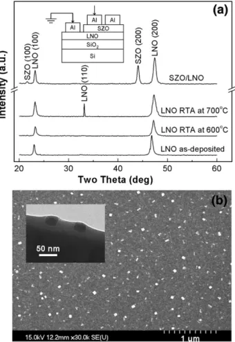
Fig. 1a shows the XRD patterns of the LNO films deposited at 250 °C and then annealed at 600 and 700 °C, and the SZO film deposited on the 600 °C-annealed LNO. The LNO and SZO films exhibit (100)-preferred orientation, which has been reported that SZO film with (100)-preferred orientation had good resistive switching behaviors [14]. In the previous researches, SrRuO3(SRO) has been popularly used for BE in
the SZO-based MIM devices[8–10]. However, in this study, the LNO BE is used owing to two reasons. Firstly, the LNO is cheaper than the SRO, which is more suitable for practical using of NVM. Secondly, the sheet resistance of a SRO film increases with the increased annealing temperature, indicating that the Fig. 1. (a) XRD patterns of LNO and SZO films. The inset is the SZO-based
MIM device structure. (b) SEM surface and TEM cross section images of the 700 °C-annealed LNO film.
Fig. 2. I–V curves of (a) pure SZO and 0.1% V:SZO, (b) 0.2 and 0.3% V:SZO, and (c) 0.4, 0.7, and 1.0% V:SZO devices. The insets in (a), (b), and (c) show their resistance ratios.
following process with high temperature will degrade the device performance. For instance, the sheet resistances of as-deposited, 650, and 750 °C-annealed SRO films are 102, 120, and 138Ω/ □, respectively. On the other hand, the sheet resistance of a LNO film decreases with the increased annealing temperature; for example, those of as-deposited, 600, 700, and 800 °C-annealed LNO films are 142, 82, 68, and 59Ω/□, respectively. The surface roughness of the 600 °C-annealed LNO film is smooth, while that of 700 °C-annealed LNO film is degraded due to the unwilling precipitates presented in the LNO surface.
Fig. 1b and the inset perform the SEM surface and TEM cross section images of the 700 °C-annealed LNO film, which clearly depict the precipitates in the LNO surface. Therefore, the 600 °C-annealed LNO film with smooth surface and low sheet resistance is very favorable for using of BE in the SZO-based MIM devices.
Fig. 2a depicts the current–voltage (I–V) curves of pure SZO and 0.1% V:SZO MIM devices. When a negative bias voltage is applied, the current of the device rapidly increases, and the device is switched from high resistance state (HRS) to low resistance state (LRS), which is defined as “turn-on” process. Otherwise, when a positive bias voltage is applied, the current of the device decreases, and the device is switched from LRS to HRS, defined as “turn-off” process. The partial turn-off phenomenon occurred in the positive voltage regime ofFig. 2
is relative to a non-uniform disruption of current paths[15]. The resistance ratios between HRS and LRS of two devices are higher than 20, which are performed in the inset ofFig. 2a.Fig. 2b and the inset perform the I–V curves and the resistance ratios
of 0.2 and 0.3% V:SZO MIM devices. The results show that the resistance ratio of the 0.3% V:SZO device is higher than 104, which is much higher than those of the less-doped devices due to the doping effect. The doping effect is achieved by Zr4+sites being substituted by V5+ leading to the suppression of the formation of oxygen vacancies, causing that the 0.3% V:SZO device has the lowest HRS current[16].Fig. 2c and the inset perform the I–V curves and the resistance ratios of 0.4, 0.7, and 1.0% V:SZO MIM devices, showing that the resistive switching properties of the 0.4 and 0.7% V:SZO devices degrade
gradually, and the switching properties disappear in the 1.0% V:SZO device, which could be due to the segregation of vanadium oxides or other compounds. Consequently, based on the experimental results, the resistive switching can be con-sidered as an intrinsic property of the SZO film, and a proper concentration of doping can improve the resistive switching properties. In addition, multi-state turn-on behavior is observed in the 0.2 and 0.7% V:SZO devices, which implies that the multi-state switching is possible for a SZO-based memory device.
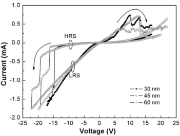
Fig. 3depicts the I–V curves of 0.2% V:SZO MIM devices
with different SZO thicknesses. The results show that the turn-on voltage is slightly dependent turn-on the SZO thickness, while the turn-off voltage is almost irrelative to the thickness. Fig. 4a depicts the endurance of the 0.3% V:SZO MIM device. The resistive switching cycle, including one turn-on and one turn-off processes, was applied on the device for more than 100 times, and the resistances of both HRS and LRS measured at−1V are shown inFig. 4a. The results show that both HRS and LRS are stable and the resistance ratio of two states holds at least 500 after applying a number of bias voltages.Fig. 4b depicts the Fig. 3. I–V curves of 0.2% V:SZO devices with different SZO thicknesses.
Fig. 4. Plots of (a) Endurance and (b) retention time of the 0.3% V:SZO device measured at−1V.
retention time of the device. During the measurement, a read voltage which cannot change the memory state was applied after a span, and the resistances of two states measured at−1V are indicated inFig. 4b. The results show that the retention time is longer than 107 s, and the resistance ratio of two states remains higher than 1000.Fig. 5a performs the non-destructive readout property of the device. More than 1000 of voltage testing cycles (from + 5V to−5V) were applied on two devices with HRS and LRS. The current of the device with LRS keeps almost unchanged, while the other declines with the increased testing cycles; therefore, the resistance ratio of two states increases with the increased cycles, which is a good tendency for accurate readout.Fig. 5b also performs the non-destructive readout property of the device. The resistances of LRS and HRS measured at both room temperature (RT) and 85 °C remain almost unchanged after continuously biased at−5V for more than 104s, which corresponds that the resistance states will not be varied after applying 1012of read pulses (assuming that the read pulse is−5V, 10 ns). Consequently, good endurance, long
Fig. 5. Non-destructive readout property of the 0.3% V:SZO device.
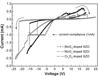
Fig. 6. Resistive switching behaviors of 0.3% MoO3-, MoO2-, and Cr2O3-doped
retention time, and non-destructive readout properties are obtained in the 0.3% V:SZO MIM devices, which is suitable for RRAM applications.
Fig. 6 shows the I–V curves of 0.3% MoO3-, MoO2-, and
Cr2O3-doped SZO MIM devices. All the devices with different
dopants perform the resistive switching behaviors. The results demonstrate again that the resistive switching is an intrinsic property of the SZO film, but proper doping concentration and element can improve the resistive switching properties. 4. Conclusions
The stable resistive switching behaviors of the sputter-deposited SZO-based MIM device are performed in this study. The LNO BE deposited at 250 °C and then annealed at 600 °C having (100)-preferred orientation performs smooth surface and high conductivity. The SZO film deposited at 500 °C also exhibits (100)-preferred orientation. The 0.3% V:SZO device depicts the best switching behaviors including high resistance ratio, high endurance, long retention time, and non-destructive readout property. The turn-on voltage is slightly dependent on the SZO thickness, while the turn-off voltage is almost irrelative to the thickness. In addition, the resistive switching properties of MoO3-, MoO2-, and Cr2O3-doped SZO devices are also studied.
Our experimental results demonstrate that the resistive switch-ing is an intrinsic property of the SZO film, but proper dopswitch-ing concentration and element can improve and stabilize the resis-tive switching behaviors. Consequently, the SZO-based mem-ory device with stable resistive switching behaviors is a possible candidate for next-generation NVM applications.
Acknowledgement
This work was supported by the Winbond Electronics Cor-poration, Taiwan, and by the National Science Council, Taiwan, under project NSC 95-2221-E009-278.
References
[1] S. Lai, T. Lowrey, Int. Electron Devices Meet. Tech. Dig. (2001) 803. [2] G.A. Prinz, Science 282 (1998) 1660.
[3] T. Hayashi, Y. Igarashi, D. Inomata, T. Ichimori, T. Mitsuhashi, K. Ashikaga, T. Ito, M. Yoshimaru, M. Nagata, S. Mitarai, H. Godaiin, T. Nagahama, C. Isobe, H. Moriya, M. Shoji, Y. Ito, H. Kuroda, M. Sasaki, Int. Electron Devices Meet. Tech. Dig. (2002) 543.
[4] A. Chen, S. Haddad, Y.C. Wu, T.N. Fang, Z. Lan, S. Avanzino, S. Pangrle, M. Buynoski, M. Rathor, W. Cai, N. Tripsas, C. Bill, M. VanBuskirk, M. Taguchi, Int. Electron Devices Meet. Tech. Dig. (2005) 746.
[5] I.G. Baek, M.S. Lee, S. Seo, M.J. Lee, D.H. Seo, D.-S. Suh, J.C. Park, S.O. Park, H.S. Kim, I.K. Yoo, U.-I. Chung, J.T. Moon, Int. Electron Devices Meet. Tech. Dig. (2004) 587.
[6] I.G. Baek, D.C. Kim, M.J. Lee, H.-J. Kim, E.K. Yim, M.S. Lee, J.E. Lee, S.E. Ahn, S. Seo, J.H. Lee, J.C. Park, Y.K. Cha, S.O. Park, H.S. Kim, I.K. Yoo, U.-I. Chung, J.T. Moon, B.I. Ryu, Int. Electron Devices Meet. Tech. Dig. (2005) 750.
[7] H. Sim, H. Choi, D. Lee, M. Chang, D. Choi, Y. Son, E.-H. Lee, W. Kim, Y. Park, I.-K. Yoo, H. Hwang, Int. Electron Devices Meet. Tech. Dig. (2005) 758.
[8] A. Beck, J.G. Bednorz, C. Gerber, C. Rossel, D. Widmer, Appl. Phys. Lett. 77 (2000) 139.
[9] C. Rossel, G.I. Meijer, D. Bremauid, D. Widmer, J. Appl. Phys. 90 (2001) 2892.
[10] J.W. Park, K. Jung, M.K. Yang, J.K. Lee, D.Y. Kim, J.W. Park, J. Appl. Phys. 99 (2006) 124102.
[11] C.Y. Liu, P.H. Wu, A. Wang, W.Y. Jang, J.C. Young, K.Y. Chiu, T.Y. Tseng, IEEE Electron Device Lett. 26 (2005) 351.
[12] Y. Watanabe, J.G. Bednorz, A. Bietsch, C. Gerber, D. Widmer, A. Beck, S.J. Wind, Appl. Phys. Lett. 78 (2001) 3738.
[13] T. Fujii, M. Kawasaki, A. Sawa, H. Akoh, Y. Kawazoe, Y. Tokura, Appl. Phys. Lett. 86 (2005) 012107.
[14] C.Y. Liu, A. Wang, W.Y. Jang, T.Y. Tseng, J. Phys., D, Appl. Phys. 39 (2006) 1156.
[15] C.C. Lin, B.C. Tu, C.C. Lin, C.H. Lin, T.Y. Tseng, IEEE Electron Device Lett. 27 (2006) 725.
[16] X. Qi, J. Dho, R. Tomov, M.G. Blamire, J.L. MacManus-Deiscoll, Appl. Phys. Lett. 86 (2005) 062903.