Thickness effects on the electrical characteristics of Ba 0.7 Sr 0.3 Ti O 3 capacitors
with nano-Cr interlayer
Chia-Cheng Ho, Bi-Shiou Chiou, and Li-Chun Chang
Citation: Applied Physics Letters 90, 132906 (2007); doi: 10.1063/1.2717553
View online: http://dx.doi.org/10.1063/1.2717553
View Table of Contents: http://scitation.aip.org/content/aip/journal/apl/90/13?ver=pdfcov Published by the AIP Publishing
Articles you may be interested in
InAs quantum wire induced composition modulation in an In 0.53 Ga 0.37 Al 0.10 As barrier layer grown on an InP substrate
J. Appl. Phys. 108, 034321 (2010); 10.1063/1.3460643
Hydrogen shuttling near Hf-defect complexes in Si Si O 2 Hf O 2 structures Appl. Phys. Lett. 91, 233503 (2007); 10.1063/1.2820380
Crystallization of Al 2 O 3 and its effects on the mechanical properties in Ti N Al 2 O 3 nanomultilayers J. Appl. Phys. 98, 074302 (2005); 10.1063/1.2067687
Formation of Mo 5 Si 3 phase in Mo/Si multilayers J. Appl. Phys. 92, 5119 (2002); 10.1063/1.1512971
Interfacial reaction in the poly- Si/Ta 2 O 5 /TiN capacitor system J. Appl. Phys. 83, 139 (1998); 10.1063/1.366732
This article is copyrighted as indicated in the article. Reuse of AIP content is subject to the terms at: http://scitation.aip.org/termsconditions. Downloaded to IP: 140.113.38.11 On: Thu, 01 May 2014 00:36:18
Thickness effects on the electrical characteristics of Ba
0.7Sr
0.3TiO
3capacitors with nano-Cr interlayer
Chia-Cheng Ho and Bi-Shiou Chioua兲
Department of Electronics Engineering, National Chiao-Tung University, Hsinchu 30010, Taiwan and Institute of Electronics, National Chiao-Tung University, Hsinchu 30010, Taiwan
Li-Chun Chang
Department of Electronics Engineering, Huafan University, Taipei 22301, Taiwan
共Received 2 November 2006; accepted 23 February 2007; published online 29 March 2007兲 A multilayer Ba0.7Sr0.3TiO3/ Cr/ Ba0.7Sr0.3TiO3 共BST/Cr/BST兲 structure was sputtered sequentially onto Pt/ Ti/ SiO2/ Si substrate. With the insertion of a 2 nm Cr interlayer, the temperature coeffi-cient of capacitance of the BST/Cr/BST dielectric is about 69% lower than that of BST monolayer dielectric. The dielectric constant and dissipation factor as the function of Cr thickness are studied. X-ray diffraction patterns, the analysis results of energy dispersive spectroscopy, and the survey scan profiles of Auger electron spectroscopy reveal the formation of a TiO2 secondary phase after the multilayer is annealed at 800 ° C in O2 atmosphere. The insertion of nano-Cr interlayer im-proves the electrical properties of BST capacitors. © 2007 American Institute of Physics. 关DOI:10.1063/1.2717553兴
BaxSr1−xTiO3 共BST兲 films are extensively investigated for applications as integrated charge-storage dielectric and electric-field tunable elements for high frequency devices. BST thin films with considerably high dielectric constant can provide the sufficient storage charge. BST films also show the low leakage current, high breakdown field, high time-dependent dielectric breakdown, and low fatigue and aging effects.1–3However, the dielectric behaviors of BST films are very temperature sensitive, and this causes crucial concern in using BST capacitors for dynamic random access memory applications.4,5
It is well known that the grain size, dielectric constant, and leakage current of the BST thin films can be modified with an underlayer and/or with appropriate dopants.6–9This is ongoing research. Our previous work indicates that the insertion of a Cr interlayer lowers the leakage current and temperature dependence of capacitance of the BST capacitor.4,5 However, the role that the nano-Cr interlayer plays on the dielectric properties of the BST films is unclear. In this study, the effects of thickness of Cr interlayer on the dielectric properties of the BST capacitors are investigated, and the root causes for the improvement of the dielectric behavior are explored.
Metal-insulator-metal 共MIM兲 capacitors with Pt/ Ba0.7Sr0.3TiO3/ Cr/ Ba0.7Sr0.3TiO3/ Pt structure were em-ployed in this study. The starting p-type Si共100兲 wafers were cleaned by the standard RCA cleaning process. After the cleaning process, 100 nm SiO2 films were grown on the Si substrate. 10 nm Ti films were sputtered onto the SiO2layer. The bottom electrodes, 100 nm Pt films, were dc sputtered at room temperature. The first Ba0.7Sr0.3TiO3共BST兲 films were then deposited using a rf magnetron sputtering at a substrate temperature of 350 ° C. The sputtering chamber was evacu-ated to a base pressure of 1⫻10−5torr initially. Then, BST films were deposited at a constant pressure of 5⫻10−3torr
which was maintained by a mixture of argon and oxygen at 9 and 3 SCCM共SCCM denotes cubic centimeter per minute at STP兲, respectively. The rf power for the deposition of both the first and second BST layers was 120 W 共power density was 2.7 W / cm2兲, and the total thickness of BST films was about 300 nm. Chromium films with various thicknesses were deposited with the same sputtering system without breaking the vacuum at the dc power of 100 W. The nominal Cr thicknesses were 2, 5, 10, and 15 nm and were monitored by the quartz crystal and the controller. The second BST films were then deposited. The BST/Cr/BST/Pt multilayer specimens were annealed at 800 ° C in O2 for 1 h and then were bombarded by O2plasma for 10 min before deposition of the top Pt electrode.
The phase of the films was characterized by an x-ray diffractometer 共XRD兲 共RU-H3R, Rigaku, Japan兲. The high resolution transmission electron microscopy 共TEM兲 共JEM-3000F, JEOL Ltd., Japan兲 was employed to observe the cross section of multilayer specimens and to measure the film thickness, and energy dispersive spectroscopy 共EDS兲 was used to identify the elemental compositions of the speci-mens. The film compositions were also investigated by Au-ger electron spectroscopy共AES兲 共Microlab 350, Thermal VG Scientific Co., England兲. An LCR meter 共HP-4285, Hewlett Packard Co., USA兲 was employed to measure the dielectric properties of the samples in the temperature range from 25 to 125 ° C.
The x-ray diffraction patterns of the 800 ° C annealed BST films with nano-Cr interlayer of various thicknesses are given in Fig.1. All BST films show crystallized cubic phase. However, a diffraction peak appears at 2= 29.73°, and this peak is identified as the共401兲 TiO2peak. The insertion of Cr layer affects the texture of the BST films. As indicated in the inset of Fig. 1, the peak ratio I共100兲/I共110兲 of BST films
increases from 8.5% of the mono-BST layer to 21.3% for BST with a 2 nm Cr interlayer and then decreases when the Cr thickness is larger than 2 nm. The 2 nm nominal film is discontinuous,5 while the 15 nm nominal Cr film shown in Fig.2共a兲is continuous, and the measured thickness is around
a兲Author to whom correspondence should be addressed; also at Innovative
Packaging Research Center, National Chiao-Tung University, Hsinchu, Taiwan; FAX: 886-3-5724361; electronic mail: [email protected]
APPLIED PHYSICS LETTERS 90, 132906共2007兲
0003-6951/2007/90共13兲/132906/3/$23.00 90, 132906-1 © 2007 American Institute of Physics This article is copyrighted as indicated in the article. Reuse of AIP content is subject to the terms at: http://scitation.aip.org/termsconditions. Downloaded to IP:
18 nm. That the continuity or discontinuity of Cr film affects the stress in the films may influence the texture of the BST films. The preferred共100兲 orientation enhances both the di-electric constant and the tunability of the BST because the Ti ion preferentially displaces along the共100兲 direction towards the oxygen ions.10
Figure 2 shows the TEM cross-section view and EDS analysis results of the BST/ Cr共15 nm兲/BST/Pt structure. The inset in Fig.2共e兲shows AES survey scan profiles for the
surface of the specimen. Formation of a thin TiO2layer for BST/Cr/BST/Pt is observed, as indicated in Fig. 2共e兲, and confirmed with the XRD results shown in Figs.1共b兲–1共e兲.
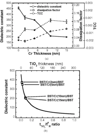
The 100 kHz dielectric constant共k兲 and dissipation fac-tor of specimens with Cr films of various thicknesses are presented in Fig.3共a兲. The dielectric constant decreases with the increase of the Cr interlayer thickness. The dissipation factor decreases initially and then increases as the thickness of Cr increases. A minimum dissipation factor of⬃0.023 is obtained for specimens with 2 nm Cr. As stated previously, a preferred 共100兲 orientation enhanced the dielectric constant of the BST films, and specimen with 2 nm Cr has enhanced 共100兲 orientation as compared to those without Cr. However, the dielectric constant of specimen with 2 nm Cr共i.e., 371兲 is smaller than that of the specimen without Cr共i.e., 456兲. It is argued that the decrease of the dielectric constant for Cr-containing specimen is attributed to the formation of the TiO2 layer. The dielectric constants of mono-TiO2 and mono-BST are 20 and 456, respectively. The curve in Fig.
3共b兲 is the calculated dielectric constants of BST/Cr/BST in series with TiO2layers of various thicknesses.11Also shown in Fig.3共b兲is the measured dielectric constant. On the basis of the calculated dielectric constant curve, the thickness of TiO2films ranges from 4.8 to 23.4 nm. The temperature co-efficient of capacitance共TCC兲 is defined as
TCC =
CT− CTr
共T − Tr兲CTr
,
where T is the temperature of interest共125 °C in this study兲,
Tr is the temperature of reference共25 °C in this study兲, and
FIG. 1. X-ray diffraction patterns of BST annealed at 800 ° C in O2with and
without the insertion of nano-Cr interlayer: 共a兲 mono-BST layer, 共b兲 BST/ Cr共2 nm兲/BST, 共c兲 BST/Cr共5 nm兲/BST, 共d兲 BST/Cr共10 nm兲/BST, and共e兲 BST/Cr共15 nm兲/BST. Inset is the ratio of I共100兲/I共110兲 as a func-tion of Cr thickness.
FIG. 2.共a兲 TEM cross-section view the BST/Cr共15 nm兲/BST MIM capaci-tor. EDS spectra of共b兲 BST bottom, 共c兲 Cr interlayer, 共d兲 BST upper, and 共e兲 TiO2phase. The inset of共e兲 shows AES survey scan profile for the surface
of BST/Cr/BST.
FIG. 3. 共a兲 Dielectric constant, dissipation factor, and temperature coeffi-cient of capacitance with nano-Cr interlayer of various thicknesses and mono-BST layer.共b兲 Calculated dielectric constants vs tTiO2/ tMratio and TiO2thickness are calculated based on the serial model共Ref.11兲. The
mea-sured dielectric constants of the BST/Cr/BST capacitors in this work are also shown. tMis the thickness of the BST/Cr/BST sample.
132906-2 Ho, Chiou, and Chang Appl. Phys. Lett. 90, 132906共2007兲
This article is copyrighted as indicated in the article. Reuse of AIP content is subject to the terms at: http://scitation.aip.org/termsconditions. Downloaded to IP: 140.113.38.11 On: Thu, 01 May 2014 00:36:18
CT and CTr are the capacitances measured at T and Tr,
re-spectively. A TCC of −5.0⫻10−4/ ° C is obtained for capaci-tors with 2 nm Cr as compared to that of −1.60⫻10−3/ ° C for capacitors with BST monolayer, as indicated in Fig.3共a兲. Insertion of nano-Cr interlayer improves the temperature sta-bility of the BST dielectric, and a positive TCC is observed for specimens with thicker than 10 nm Cr. The negative TCC of BST is compensated by the positive TCC of the TiO2.12It is believed that the formation of the TiO2 films affects the dielectric constant, dissipation factor, and TCC of the speci-mens. The thermal stability of the dielectric is enhanced with the implementation of the nano-Cr interlayer. However, the mechanism for the formation of TiO2 in the presence of nano-Cr interlayer is subjected to further study.
In summary, the MIM capacitors with BST/Cr/BST multilayer dielectric are investigated. The insertion of the 2 nm Cr improves both the dissipation factor and TCC of the capacitors. A TCC of −5.0⫻10−4/ ° C from 25 to 125 ° C is obtained for BST/Cr/BST as compared to that of −1.60⫻10−3/ ° C for mono-BST films. Besides, a dissipation factor of 0.023 at 100 kHz is obtained for BST/Cr/BST ca-pacitors as compared to that of 0.028 for mono-BST capaci-tor. Although the dielectric constant decreases from 456 to 371 with the implementation of the 2 nm Cr layer, the tem-perature stability of the capacitor is improved. Formation of
a TiO2 layer in series with the BST/Cr/BST structure is ar-gued to be one of the reasons for the change in the electrical characteristics of the capacitors.
This work is sponsored by National Science Council, Taiwan, under Contract No. NSC 95-2221-E-009-085.
1D. C. Shye, B. S. Chiou, M. J. Lai, C. C. Hwang, C. C. Jaing, J. S. Chen,
M. H. Cheng, and H. C. Cheng, J. Electrochem. Soc. 150, F20共2003兲.
2D. C. Shye, B. S. Chiou, M. W. Kuo, J. S. Chen, B. C. S. Chou, C. C.
Jaing, M. F. Wu, and H. C. Cheng, Electrochem. Solid-State Lett. 6, G55 共2003兲.
3J. W. Liou and B. S. Chiou, J. Mater. Sci.: Mater. Electron. 11, 637
共2000兲.
4C. C. Ho, B. S. Chiou, L. C. Chang, C. C. Chou, B. H. Liou, and C. C. Yu,
Surf. Coat. Technol. 201, 4163共2006兲.
5M. W. Kuo, D. C. Shye, B. S. Chiou, J. S. Chen, and H. C. Cheng, Integr.
Ferroelectr. 61, 183共2004兲.
6W. C. Yi, T. S. Kalkur, E. Philofsky, and L. Kammerdiner, Thin Solid
Films 402, 307共2002兲.
7S. Y. Chen, H. W. Wang, and L. C. Huang, Jpn. J. Appl. Phys., Part 1 40,
4974共2001兲.
8K. T. Kim and C. I. Kim, Thin Solid Films 472, 26共2005兲.
9K. H. Yoon, J. C. Lee, J. Park, D. H. Kang, C. M. Song, and Y. G. Seo,
Jpn. J. Appl. Phys., Part 1 40, 5497共2001兲.
10Y. Xia, D. Wu, and Z. Liu, J. Phys. D 37, 2256共2004兲.
11J. J. Si, H. Ono, K. Uchida, H. Morisaki, and N. Itoh, Appl. Phys. Lett. 79, 3140共2001兲.
12A. G. Cockbain and P. J. Harrop, J. Appl. Phys. 1, 1109共1968兲.
132906-3 Ho, Chiou, and Chang Appl. Phys. Lett. 90, 132906共2007兲
This article is copyrighted as indicated in the article. Reuse of AIP content is subject to the terms at: http://scitation.aip.org/termsconditions. Downloaded to IP: 140.113.38.11 On: Thu, 01 May 2014 00:36:18